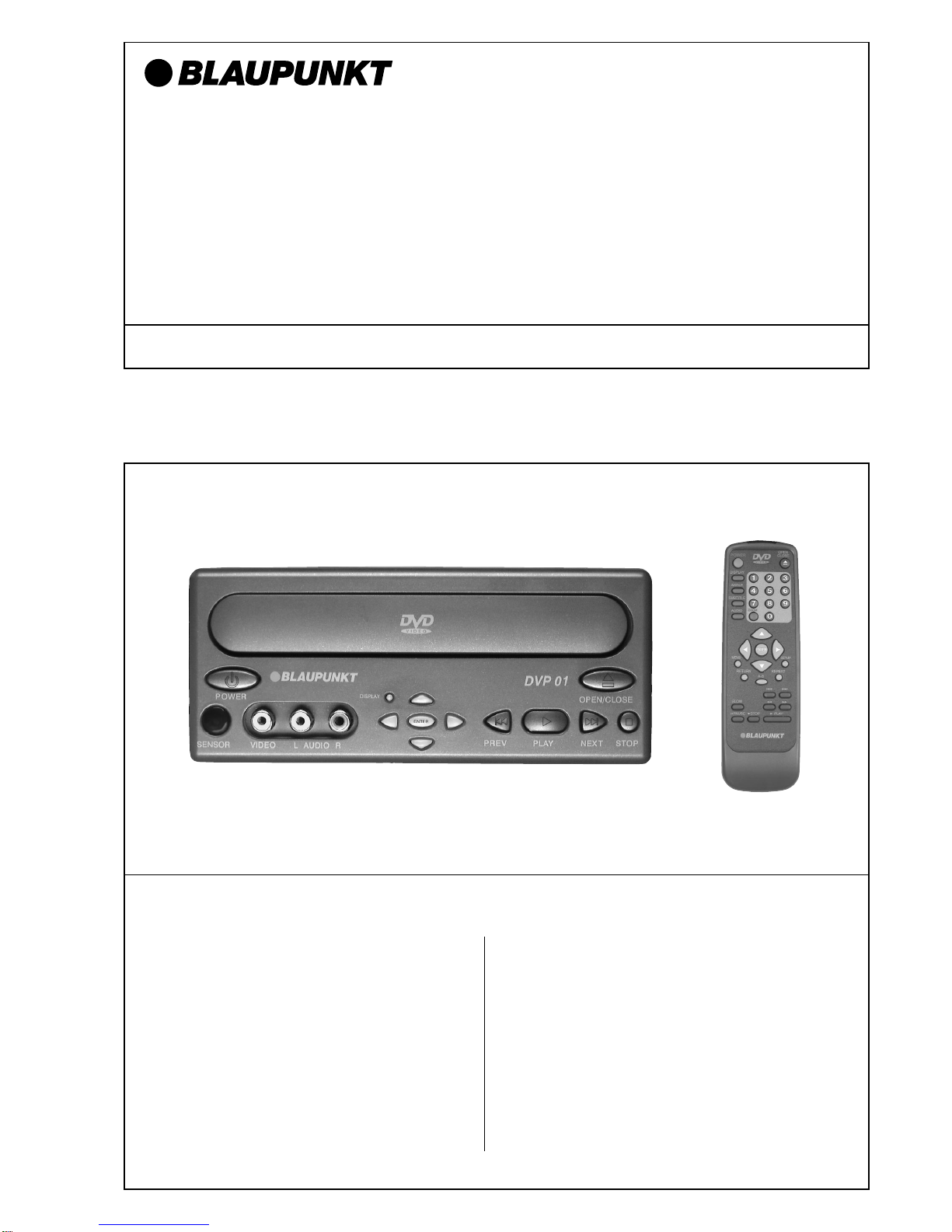
Blaupunkt DVP 01 User manual

MOBILE VIDEO SYSTEMS
CM/PSS 8 622 402 868 11/01
Schaltbild • Circuit diagram
Inhaltsverzeichnis Seite
Bedienelemente 2-3
Technische Daten 4
Sicherheitshinweise 4
Blockdiagramm 5
Fehlersuchpläne 6-9
IC Block Diagramme 10-18
Bestückte Platten 19-21
Interne Steckverbindungen 22
Schaltbilder 23-36
Explosionszeichnung 37
DVD PLAYER
DVP 01, 12/24V
PAL / NTSC
7 607 276 007
Table of Contents Page
Controls 2-3
Technical data 4
Safety informations 4
Block diagram 5
Troubleshooting charts 6-9
IC Block diagrams 10-18
Component boards 19-21
Internal connectors 22
Schematic diagrams 23-36
Exploded view 37

- 2 -
Bedienelemente
1
2
3
4
5
26
25
24
23
22
20 21
19
17 18
16
15
6
8
7
9
10
11
12
13
14
28 15 19
30 129
8
2
27
21
724 23 18 26 14
33 34
32 35
31
Controls

- 3 -
Bedienelemente
Controls
1POWER button - to switch
the unit on/off
2DISPLAY button - to show/
hide the status bar on the
monitor
3ANGLE button - to select a
camera angle
4SUBTITLE button - to select
film subtitles
5AUDIO button - to select the
film language
6ZOOM button - to enlarge a
screen section during
playback
7button - to move the
selection pointer in menus
8button - to move the
selection pointer in menus
9MENU button - to open a
DVD’s main menu
:RETURN button - to exit a
menu item in a menu
;A-B button - to mark a
custom sequence on a DVD
<SLOW button - to start/stop
slow motion
=PAUSE button - to pause
playback
>STOP button - to stop
playback
?PLAY button - to start
playback
@button - to fast rewind
Abutton - to fast forward
Bbutton - to skip to the start
of the chapter
Cbutton - to skip to the
start of the next chapter
DREPEAT button - to repeat a
chapter or title of a film
Ebutton - to move the
selection pointer in menus
FSETUP button - to open the
setup menu of the DVP 01
Gbutton - to move the
selection pointer in menus
HENTER button - to select
menu items
I0-9 buttons - to enter
numbers
JOPEN/CLOSE button - to
open and close the drive
drawer
KDrive drawer
LAUDIO inputs - to connect an
external audio source
MVIDEO input - to connect an
external video source
NSENSOR - IR remote control
sensor
OS-VIDEO OUTPUT - S-VHS
output
PVIDEO output - to connect a
monitor
QAUDIO outputs - to connect a
Blaupunkt audio system
RWIRE REMOTE - to connect
a cable remote control
(option)
SDC 12V/24V input - to
connect the DVP 01 to a 12
V / 24 V voltage source
1POWER-Taste, zum Ein-/
Ausschalten des Gerätes
2DISPLAY-Taste, zum Ein-/
und Ausblenden der Status-
leiste auf dem Monitor
3ANGLE-Taste, zur Auswahl
einer Kameraperspektive
4SUBTITLE-Taste, zur
Auswahl von Untertiteln für
einen Film
5AUDIO-Taste, zur Auswahl
der Sprache für einen Film
6ZOOM-Taste, zur Aus-
schnittvergrößerung wäh-
rend der Wiedergabe
7-Taste, zum Verschieben
der Auswahlmarkierung in
Menüs
8-Taste, zum Verschieben
der Auswahlmarkierung in
Menüs
9MENU-Taste, zum Aufrufen
des Hauptmenüs einer DVD
:RETURN-Taste, zum Verlas-
sen eines Menüpunktes in
einem Menü
;A-B-Taste, zum Markieren
einer selbstgewählten
Passage einer DVD
<SLOW-Taste, zum Starten
und Beenden der Zeitlupe
=PAUSE-Taste, zum Unter-
brechen der Wiedergabe
>STOP-Taste, zum Beenden
der Wiedergabe
?PLAY-Taste, zum Starten
der Wiedergabe
@-Taste, schneller Rück-
lauf
A-Taste, schneller Vorlauf
B-Taste, zum Anfang des
Kapitels wechseln
C-Taste, zum Anfang des
nächsten Kapitels wechseln
DREPEAT-Taste, Kapitel oder
Abschnitt eines Films wie-
derholt abspielen lassen
E-Taste, zum Verschieben
der Auswahlmarkierung in
Menüs
FSETUP-Taste, Setup-Menü
des DVP 01 aufrufen
G-Taste, zum Verschieben
der Auswahlmarkierung in
Menüs
HENTER-Taste, zum Auswäh-
len von Menüeinträgen
I0-9-Tasten, zur Eingabe von
Zahlen
JOPEN/CLOSE-Taste, zum
Öffnen und Schließen der
Laufwerksschublade
KLaufwerksschublade
LAUDIO-Eingänge, zum
Anschluß einer externen
Audioquelle
MVIDEO-Eingang, zum
Anschluß einer externen
Videoquelle
NSENSOR, Empfänger der
IR-Fernbedienung
OS-VIDEO OUTPUT, S-VHS-
Ausgang
PVIDEO-Ausgang, zum
Anschluß an einen Monitor
QAUDIO-Ausgänge, zum
Anschluß an eine Blaupunkt-
Audioanlage
RWIRE REMOTE, zum
Anschluß einer Kabel-
fernbedienung
(Option)
SDC 12V/24V Eingang, zum
Anschluß des DVP 01 an
eine
12 V/24 V-Spannungsquelle

- 4 -
Technische Daten
GENERAL
Operating voltage: 12 V/ 24 V
Power consumption: 20 W
Current consumption
In operation: 800mA
Stand by: 50mA
Operating temperature: -15°C – +60°C
Humidity: 10 % – 90 %
Dimensions (WxHxD): 170 x 73 x 245 mm
Weight:approx. 2.3 kg
VIDEO/AUDIO
Tv colour standards: PAL/NTSC
Laser CLASS II (DVD): 650 nm
(CD,VCD): 780 nm
Video resolution (PAL): 720 Pixel hor. x 576 Pixel vert.
(NTSC): 720 Pixel hor. x 480 Pixel vert.
Frequency ranges
Video: 5 MHz / -2dB
Audio: 20 Hz - 20 kHz
Output level Video: 1 Vss, 75 Ω
Audio: 2 Veff, 100 Ω
ALLGEMEIN
Betriebsspannung: 12 V/ 24 V
Leistungsaufnahme: 20 W
Stromaufnahme
Betrieb: 800mA
Stand by: 50mA
Betriebstemperatur: -15°C – +60°C
Luftfeuchtigkeit: 10 % – 90 %
Abmessungen BxHxT: 170 x 73 x 245 mm
Masse: ca. 2,3 kg
VIDEO/AUDIO
Fernsehsystem: PAL/NTSC
Laser CLASS II (DVD): 650 nm
(CD,VCD): 780 nm
Video Auflösung (PAL): 720 Pixel hor. x 576 Pixel vert.
NTSC): 720 Pixel hor. x 480 Pixel vert.
FrequenzbereichVideo: 5 MHz / -2dB
Audio: 20 Hz - 20 kHz
Ausgangspegel Video: 1 Vss, 75 Ω
Audio: 2 Veff, 100 Ω
Sicherheitshinweise
Das Gerät ist mit einem Laser ausgestattet. Im
Service-Betrieb beachten Sie bitte folgende Hin-
weise:
•Schauen Sie bei geöffnetem Gerät niemals in
den Laser (unsichtbarer Laserstrahl).
•Tragen Sie bei allen Arbeiten am Laser eine
Laser-Schutzbrille.
Safety instructions
This system is equipped with a laser unit. To
service the unit, please observe the following
instructions:
•After having opened the enclosure, never look
into the laser directly (invisible beam).
•Make sure to wear laser safety goggles for all
works on the unit.
Technical data

- 5 -
Block Diagramm Block diagram

- 6 -
Fehlersuchplan Trouble shooting
Power circuit
A. Checking the power circuit
Check T201
No 12 V Voltage
Check F 201 Fuse
Check DW 201
Check Q 202.Q 203.
Q 205
Check Q 201
No 5 V Voltage
Check Q 201
Output is 12 V
No 9 V OUT
Check IC 202
Check CZ 201
Check IC 201
Check the power
supply is DC 10-16
YES
YES
YES
YES
YES
YES
YES

- 7 -
Fehlersuchplan Trouble shooting
Power circuit
B. Push button is not good
Check Switch button IF other button
Check IC U 32
IF power button
YES
YES
Check P 19 of
IC U 32 is high
YES
Check IC 102
YES
YES
Check XPK 1

- 8 -
C. Remote control is not good
YES
YES
Wire control
D. No response after press wire control key
Fehlersuchplan Trouble shooting
Check if the sensor IR output
have a low, when control
Check Q 1 (78L05)
Output is 5 V
Check the sensor
Check Q 1
Check CR 1
Check IC U 32
Check CP 4, C 3
Check D 202, D 201
Check QP 01
OK

- 9 -
NO VIDEO
Check IC 201, IC 202
Check X 1, X 3
Check IC U 5
Check IC U 9
Check IC U 10, U 11, U 7
Check IC U 15, U 16, U 18
Check IC U 31
Check J 17
Check J 11, J 12
OK
OK
OK
OK
OK
OK
OK
OK
NO AUDIO
Check IC U 23
Check J 15, J 16
Check J 11
OK
Fehlersuchplan Trouble shooting
E. Audio and Video circuit

- 10 -
IC Block Diagramm IC Block diagram
1. NC 11. VCC
2. SCK1 12. V OUTL
3. TEST 13. CAP
4. ML 14. BCKIN
5. MC 15. DIN
6. MD 16. LRCIN
7. RSTB 17. GND
8. ZERO 18. NC
9. VOUTR 19. VDD
10. AGND 20. DGND
PCM 1720

- 11 -
IC Block Diagramm IC Block diagram
1. FSADJUST 14. RGBOUT 27. TTXDAT 40. SDA
2. VBIAS 15. FIELD 28. P0 41. SCL
3. VREF 16. Y0 29. P1 42. SLAVE
4. VAA 17. Y1 30. P2 43. CLK
5. COMP 18. Y2 31. P3 44. VDD3V
6. AGND 19. Y3 32. P4 45. GND
7. AGND 20. Y4 33. P5 46. VDD
8. CVBS/B 21. Y5 34. P6 47. RESET
9. AGND 22. GND 35. P7 48. BLANK
10. CVBS/G 23. VDD 36. GND 49. VSYNC
11. AGND 24. Y6 37. VDD 50. HSYNC
12. C/R 25. Y7 38. TTXREQ 51. AGND
13. Y/CVBS 26. ALTADDR 39. SLEEP 52. AGND
BT864A/865A

- 12 -
IC Block Diagramm IC Block diagram
AM188EM-33KC
1. SDEN1 21. VCC 41. GND 61. VCC 81. AD9
2. SDEN0 22. A17 42. WHB 62. PCS3 82. AD2
3. SCLK 23. A16 43. WLB 63. PCS2 83. AD10
4. BHE/ADEN 24. A15 44. HLDA 64. GND 84. AD3
5. WR 25. A14 45. HOLD 65. PCS1 85. AD11
6. RD 26. A13 46. SRDY 66. PCS0 86. AD4
7. ALE 27. A12 47. NMI 67. VCC 87. AD12
8. ARDY 28. A11 48. DT/R 68. MCS2 88. AD5
9. S2 29. A10 49. DEN 69. MCS3/RFSH 89. GND
10. S1 30. A9 50. MCS0 70. GND 90. AD13
11. S0 31. A8 51. MCS1 71. RES 91. AD6
12. GND 32. A7 52. INT4 72. TMRIN1 92. VCC
13. X1 33. A6 53. INT3/INTA1/IRQ 73. TMROUT1 93. AD14
14. X2 34. A5 54. INT2/INTA0 74. TMROUT0 94. AD7
15. VCC 35. A4 55. INT1/SELECT 75. TMRIN0 95. AD15
16. CLKOUTA 36. A3 56. INT0 76. DRQ1 96. S6/CLKDIV2
17. CLKOUTB 37. A2 57. UCS/ONCE1 77. DRQ0 97. UZI
18. GND 38. VCC 58. LCS/ONCE0 78. AD0 98. TXD
19. A19 39. A1 59. PCS6/A2 79. AD8 99. RXD
20. A18 40. A0 60. PCS5/A1 80. AD1 100. SDATA

- 13 -
IC Block Diagramm IC Block diagram
ATF1500A/AL
1. I/O 23. VCC
2. GND 24. I/O
3. VCC 25. I/O
4. I/O 26. I/O
5. I/O 27. I/O
6. I/O 28. I/O
7. I/O 29. I/O
8. I/O 30. GND
9. I/O 31. I/O
10. GND 32. I/O
11. I/O 33. I/O
12. I/O 34. I/O
13. I/O 35. VCC
14. I/O 36. I/O
15. VCC 37. I/O
16. I/O 38. I/O
17. I/O 39. I/O
18. I/O 40. I/O
19. I/O 41. I/O
20. I/O 42. GND
21. I/O 43. I/O
22. GND 44. GND

- 14 -
IC Block Diagramm IC Block diagram
ZiVA-3CR
1. PIO0
2. HATA0
3. HATA1
4. HATA2
5. E_VDD
6. HATA3
7. E_VSS
8. HDATA4
9. HDATA5
10. HDATA6
11. HDATA7
12. I_VDD
13. RESET
14. I_VSS
15. WAIT/DTACK
16. INT
17. E_VDD
18. AMOE
19. E_VSS
20. AMWE
21. AMDATA0
22. AMDATA1
23. AMDATA2
24. AMDATA3
25. AMDATA4
26. AMDATA5
27. E_VDD
28. AMDATA6
29. E_VSS
30. AMDATA7
31. AMADDR0
32. AMADDR1
33. AMADDR2
34. AMADDR3
35. AMADDR4
36. E_VDD
37. AMADDR5
38. E_VSS
39. AMADDR6
40. I_VDD
41. AMADDR7
42. I_VSS
43. AMADDR8
44. AMADDR9
45. AMADDR10
46. AMADDR11
47. E_VDD
48. AMADDR12
49. E_VSS
50. AMADDR13
51. AMADDR14
52. PIO1
53. MDATA15
54. MDATA0
55. E_VDD
56. MDATA14
57. E_VSS
58. MDATA1
59. MDATA13
60. MDATA2
61. E_VDD
62. MDATA12
63. E_VSS
64. MDATA3
65. I_VDD
66. MDATA11
67. I_VSS
68. MDAT4
69. E_VDD
70. MDATA10
71. E_VSS
72. MDATA5
73. MDATA9
74. MDATA6
75. E_VDD
76. MDATA8
77. E_VSS
78. MDATA7
79. LDQM
80. UDQM
81. E_VDD
82. MWE
83. E_VSS
84. SD-CLK
85. SD-CAS
86. SD-RAS
87. E_VDD
88. SD-CS1
89. E_VSS
90. SD-CS0
91. I VDD
92. EDO-CAS
93. I VSS
94. EDO-RAS
95. E_VDD
96. MADDR9
97. E_VSS
98. MADDR11
99. MADDR8
100. MADDR10
101. E_VDD
102. MADDR7
103. E_VSS
104. MADDR0

- 15 -
IC Block Diagramm IC Block diagram
ZiVA-3CR
105. MADDR6
106. MADDR1
107. E_VDD
108. MADDR5
109. E_VSS
110. MADDR2
111. MADDR4
112. MADDR3
113. E_VDD
114. MADDR12
115. E_VSS
116. MADDR13
117. I_VDD
118. MADDR14
119. I_VSS
120. MADDR15
121. MADDR16
122. MADDR17
123. E_VDD
124. MADDR18
125. E_VSS
126. MADDR19
127. MADDR20
128. ROM-CS
129. PIO2
130. NC
131. E_VDD
132. E_VDD
133. PIO3
134. E_VDD
135. E_VDD
136. E_VSS
137. E_VDD
138. PIO4
139. E_VDD
140. E_VDD
141. PIO5
142. VDATA0
143. VDATA1
144. I_VDD
145. VDATA2
146. I_VSS
147. PIO6
148. VDATA3
149. E_VDD
150. VDATA4
151. E_VSS
152. VDATA5
153. PIO7
154. VDATA6
155. VDATA7
156. PIO8
157. HSYNC
158. VSYNC
159. DA-IEC
160. E_VDD
161. DA-DATA0
162. E_VSS
163. DA-DATA1
164. DA-DATA2
165. DA-DATA3
166. DA-LRCK
167. DA-BCK
168. I_VDD
169. DA-XCK
170. I_VSS
171. DAI-DATA
172. DAI-LRCK
173. DAI-BCK
174. PIO9
175. E_VDD
176. A_VDD
177. VCLK
178. SYSCLK
179. A_VSS
180. DVD-DATA0/CD-DATA
181. E_VDD
182. DVD-DATA1/CD-LRCK
183. E_VSS
184. DVD-DATA2/CD-BCK
185. DVD-DATA3/CD-C2PO
186. DVD-DATA4/CDG-SDATA
187. DVD-DATA5/CDG-VFSY
188. DVD-DATA6/CDG-S0S1
189. DVD-DATA7/CDG-SCLK
190. PIO0
191. VREQUEST
192. VSTROBE
193. E_VDD
194. AREQUEST
195. E_VSS
196. V_DACK/ASTROBE
197. I_VDD
198. A_DACK
199. I_VSS
200. ERROR
201. HOST8SEL
202. HADDR0
203. HADDR1
204. HADDR2
205. DTACKEL
206. CS
207. R/W
208. RD

- 16 -
IC Block Diagramm IC Block diagram
ZiVA-3CR IC COM PORT
Port Name Pin NO. Type Port Description
System services
RESET P13 I Hardware reset. An external device asserts RESET
(active LOW) to execute a decoder hardware reset. TO
ensure proper initialization after power stable, assert
RESET for at least 20 us.
SYSCLK P178 I System clock, Decoder requires an external 27 MHz TTL
Oscillator. Drive with the same 27-MHz as VCK.
PIO(10:0) P190.174.156.153.14.7. I/O Programmable I/O pins.
141.138.133.129.52.1
Power and Ground
A-VDD P176 Analog 3.3-V analog supply voltage.
Power
A-VSS P179 Analog Analog ground for PLL
Ground
VDD P5.12.17.27.36.40.47. Power 3.3-V supply voltage for core logic and I/O Signals.
55.61.65.69.75.81.87.
91.95.101.107.113.
117.123134.144.149
160.168.181.193.197
VSS P7.14.19.29.38. 42. 49. Ground Ground for core logic and I/O signals.
57.63.67. 71.77. 83.
89.93.97.103.109. 115.
119.125.136.146. 151.
162.170.183.195.199
8-bit Host Interface
CS P206 I Host chip select. Host asserts CS select the decoder for
a read or write operation. The falling edge of this signal
Triggers the read or write operation.
DTACKSEL P189 I Tie HIGH to select WAIT signal, LOW to select DTACK
Signal (Motorola 68k mode).
HADDR(2:0) P202-204 I Host address bus 3-bit address bus selects one of eight
Host interface registers.
HDATA(7:0) P2-4,6,8-11 I/O 8-bit bi-directional host data bus. Host writes data to the
Decoder Code FIFO via HDATA (7:0). MSB of the
32-bit word is written first. The host also reads and
writes the decoder internal registers and local SDRAM/
ROM via HDATA(7:0).
HOST8SEL P201 I Drive HIGH to Select 8-bit, LOW to select 16-bit host
16-bit host interface.
INT P16 0,0D, Host interrupt. Open drain signal, must be pulled-up to
PU 3.3 volts.
RD P208 I Read strobe in I mode. Must be held HIGH in M Mode
R/W P207 I Read/write strobe in M mode. Write strobe in I mode.
Host asserts R/W LOW to select write and LOW to
Select Read.
WAIT/DTACK P15 0.0D. Transfer not complete / data acknowledge. Active LOW
PU To indicate host initiated transfer is not complete. WATT
Is asserted after the falling edge of CS and reasserted
When decoder is ready to complete transfer cycle.
Open drain signal. Must be pulled-up to 3.3 volts.

- 17 -
Port Name Pin NO. Type Port Description
Parallel DVD/CD or Serial CD Interface
AREQUEST P194 O Audio request. Decoder asserts AREQUEST to indicate
that the audio input buffer has available space.
ADACK P198 I Audio data acknowledge.
DVD-DATA P186-189 I DVD parallel compressed data from DVD DSP. When
(7:4) DVD DSP sends 32-bit words. It must write the MSB first
DVD-DATA3/ P185 I Asserted HIGH indicates a corrupted byte. Decoder
CD-C2P0 keeps The previous valid picture on-screen until the next
valid Picture is decoded. This pin is shared with DVD
Compressed data DVD-DATA3.
DVD-DATA2/ P184 I CD bit clock. Decoder accept multiple BCK rates. This pin
CD-BCK Is shared with DVD compressed data DVD-DATA2.
DVD-DATA1/ P182 I Programmable polarity 16-bit word synchronization to the
CD-LRCK Decoder (right channel HIGH). This pin is shared with
DVD compressed data DVD-DATA1)
DVD-DATA0/ P180 I Serial CD data. This pin is shared with DVD compressed
CD-DATA Data DVD-DATA0
ERROR P200 I Error in input data. If ERROR signal is not available from
The DSP it must be grounded through a 4.7K resistor.
VDACK P196 I Video data acknowledge. Asserted when DVD data is
valid. Polarity is programmable.
VREQUEST P191 O Video request. Decoder asserts REQUEST to indicate
that The video input buffer has available space. Polarity
is Programmable
VSTROBE P192 I Video strobe. Programmable dual mode pulse.
Asynchronous and synchronous. In Asynchronous mode,
an external source pulses VSTROBE to indicate data is
ready for transfer. In synchronous mode VSTROBE
clocks data.
Video Output
HSYNC P157 I/O Horizontal sync. The decoder begins outputting pixel
data for a new horizontal line after the falling (active)
edge of HSYNC.
VCLK P177 I Video clock. Clocks out data on input. VDATA(7:0).
Clock is typically 27 MHz.
VDATA(7:0) P142.143.145.148 O Video data bus. Byte serial CbYCrY data synchronous
150.152.154.155 With VCLK. At power-up, the decoder initially drives
VDATA. Any other device attached to the video bus must
be 3-stated when the decoder is powered-up. During
Boot-up, the decoder initializes to 3-state VDATA: but
For a brief period it drives VDATA.
VSYNC P158 I/O Vertical sync. Bi-directional, the decoder outputs the top
Border of a new field on the first HSYNC after the
falling Edge of VSYNC. VSYNC can accept vertical
synchronization or top/bottom field notification from an
external source. (VSYNC HIGH = bottom field. VSYNC
LOW = Top field)
IC Block Diagramm IC Block diagram

- 18 -
IC Block Diagramm IC Block diagram
Port Name Pin NO. Type Port Description
OSD Interface
OSD-BLK1 P139 I Black out OSD.
OSD-CLK P130 O 27I 2 or 27 I4 MHz clock.
OSD-DATA(3:0) P131.132.135.137. I External OSD color look-up data.
OSD-VC1 P140 I Transparent OSD.
SDRAM/ROM Interface
EDO-CAS P92 O EDO CAS.
EDD-RAS P94 O EDO RAS.
LDQM P79 O SDRAM LDQM.
MADDR(20:0) P96.98-100.102.104-106. O Memory address.
108.110-112.114.116.118.
120-122.124.126.127
MDATA(15:0) P53.54.56.58-60.62.64.66. I/O Memory data.
68.70.72-74.76.78
MWE P82 O SDRAM/EDO write enable Decoder asserts active LOW
To request a write operation to the SDRAM array
ROM-CS P128 O ROM chip select.
SD-CAS P85 O Active LOW SDRAM column address.
SD-CLK P84 O SDRAM system clock.
SD-CS(1:0) P88.90 O Active LOW SDRAM bank select.
SD-RAS P86 O Active LOW SDRAM row address.
UDQM P80 O SDRAM UDQM.
Audio Interface
DA-BCK P167 O PGM bit clock. Divided by 8 from DA-XCK can be either
48 or 32 times the sampling clock.
DA-DATA P161.163.165. O PCM data our, six channels. Serial audio samples relati-
(3:0) ve to DA-BCK clock. Resulting in downmixed audio
output.
DA-LRCK P166 O PCM left-right clock. ldentifies the channel for each audio
sample. The polarity is programmable.
DA-XCK P169 I/O Audio external frequency clock. Used to generate DA-
BCK and DA-LRCK. DA-XCK can be either 384 or 256
times The sampling frequency.
DAI-BCK P173 I PCM input bit clock.
DAI-DATA P171 I PCM input data, two channels. Serial audio samples
relative to DA-BCK clock, resulting downmixed audio
output
DAI-LRCK P172 I PCM input left-right clock.
IEC958 P159 O Bitstream or PCM data out in IEC-958 format.
Audio SDRAM Interface (Optional)
AMADDR P31-35.37.39.41. O Audio SDRAM address bus.
(14:0) 43-46.48.50.51
AMDATA(7:0) P21-26-28.30 I/O Audio SDRAM data bus.
AMOE P18 O Audio SDRAM output enable.
AMWE P20 O Audio SDRAM write enable.

Netzteilplatte
Power adapter board
Bedienteilplatte
Front panel
Bestückte Platten Component boards
- 19 -

Hauptplatte
Main board
Bestückte Platten Component boards
- 20 -
Other manuals for DVP 01
2
Table of contents
Other Blaupunkt DVD Player manuals

Blaupunkt
Blaupunkt TEV-501 User manual

Blaupunkt
Blaupunkt DVD-ME1 User manual

Blaupunkt
Blaupunkt DVD-ME1 User manual

Blaupunkt
Blaupunkt MVP 01 User manual

Blaupunkt
Blaupunkt DVP 01 User manual

Blaupunkt
Blaupunkt BDVD20H User manual

Blaupunkt
Blaupunkt DVP 01 User manual

Blaupunkt
Blaupunkt BDVD5200H User manual