BMC PS2000TL+ User manual

V1.31

TableofContents
1. Features --------------1
--------------2
2. How to Install Roll Paper
2-1 Specification of thermal roll paper --------------1
2-2 Step of changing --------------1
2-3 How to removing paper after paper jamming --------------2
2-5 How to adjust paper near-end sensor --------------2
3. How to change the memory back-up battery --------------1
4. Operation for maintenance
4-1 System reset --------------1
4-2.Cancel password of the control lock mode
4-3 Display program version --------------1
4-4 All RAM memory clear --------------1
4-5 Communication port loop-back test --------------2
4-6. E-PROM CHECK-SUM Printing --------------3
5. Logic Circuit
5-1 Connection Diagram --------------1
5-2 Block Diagram --------------2
5-3 Primary power circuit --------------3
5-4 Power circuit --------------4
5-5 Power failure & Reset signal generation circuit--------------5
5-6 Battery charge & Voltage checking circuit --------------5
5-7 Memory selection circuit --------------6
5-8 I/O selection circuit --------------7
5-9 Real-Time clock circuit --------------8
5-10 Buzzer circuit --------------8
5-11 Drawer circuit --------------9
5-12 Key scan circuit --------------10
5-13 Keyboard physical position & Matrix
for Conversion key type --------------11
5-14 Keyboard physical position & Matrix
for Flat key type --------------12
5-15 LCD display circuit --------------13
5-16 VFD display circuit --------------14
5-17 Thermal printer circuit --------------15
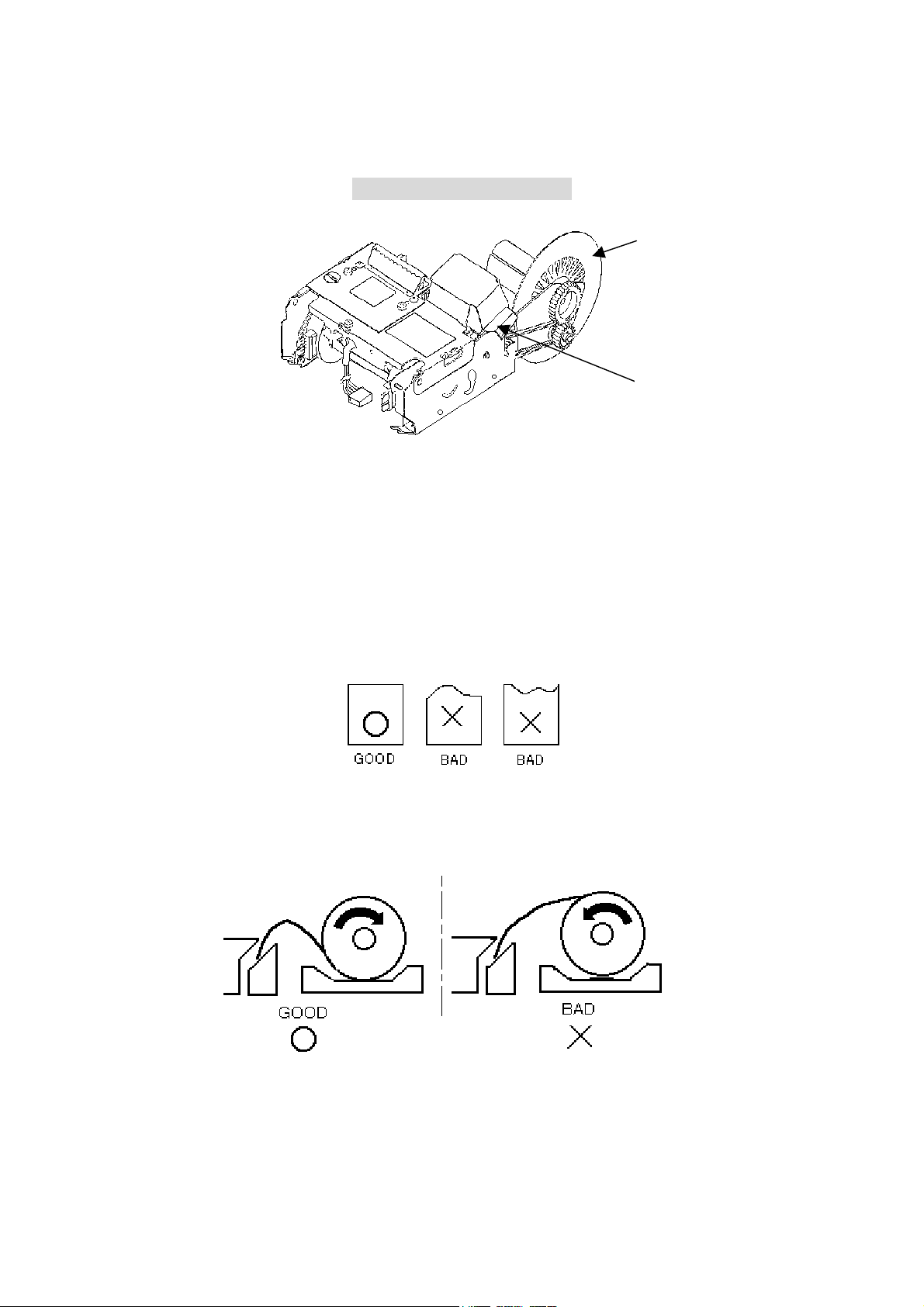
6. Printer Maintenance
6-1 Cleaning --------------1
6-2 Inspection --------------1
6-3 Lubrication --------------2
6-3-1 Type of Lubricant --------------2
6-3-2 Lubrication standards --------------2
6-4 Tools & Jigs
6-4-1 List of Tools --------------2
6-5 Troubleshooting of printer
6-5-1 Repair Levels --------------3
6-5-3 Repair Procedure --------------3
6-6 Head Connector --------------8

TableofContents
7. Parts List
7-1 M-T245 Printer --------------1
7-2 Main board Assy --------------4
7-3 Front Display board Assy --------------7
7-4 Rear Display board Assy --------------8
7-5 AC Line Noise Filter board Assy --------------8
7-7 Keyboard Assy --------------9
7-8 Housing Assy -------------12
7-9 Printer Assy -------------14
7-10 Others --------------14
8 Circuit Diagram
8-1 Main board 1/4
8-2 Main board 2/4
8-3 Main board 3/4
8-4 Main board 4/4
8-5 Front display board
8-6 AC Line Noise Filter board
8-7 Back Display board
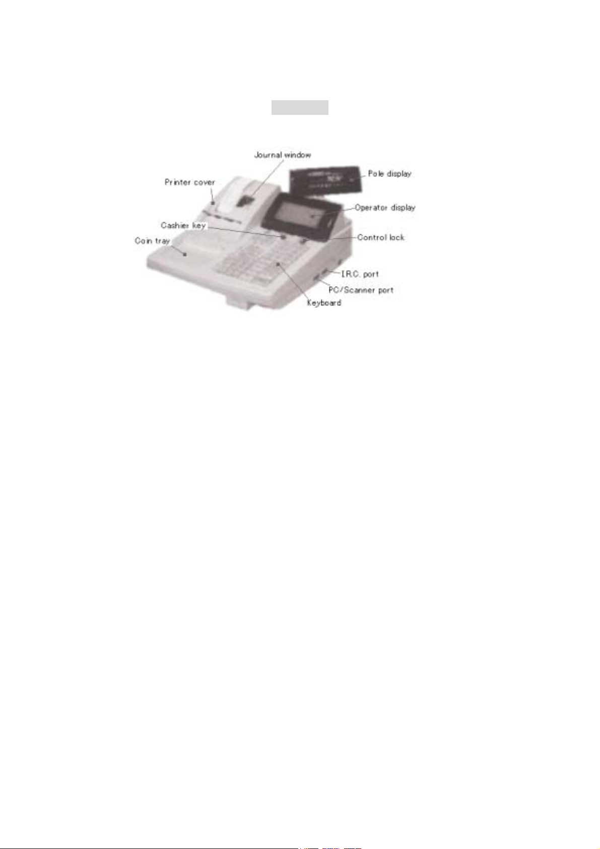
1. Features
The PS2000TL+ is an excellent electric cash register that is equal to a P.O.S. system.
It’s loaded a two-station heavy-duty thermal printer with auto cutter and four lines big
size LCD display with back-light for operator. The general hardware specifications
are as follows.
1-1. Printer Head 2 Station Line Thermal EPSON M-T245
MCBF : 500Mil Lines
Paper Width Receipt 45mm /Journal 45mm x 80φ(Max)
Thermal Head 8 dots /mm
Printing Speed About 17 Line/Sec
Auto Cutter Standard ( Full & Partial Cut)
MCBF:330,000Cut
Paper End Sensor Receipt & Journal
Paper Near End Sensor Receipt & Journal
Paper Auto Loading Available
1-2. Display
1-2-1 Operator Display 20 x 4 Line LCD with Back-light
View Area 123.0 (W) x 42.5(H)
Character Size 4.84 x 9.22 mm
1-2-2 Customer Display Numeric VFD
2-3 External Display (Option) 20 Alpha x2 Line LCD/VFD
1-3. Keyboard
Conventional Keyboard Type 80 keys Matrix
Flat Keyboard Type 173 keys Matrix
1-4. Operation Key
Control Lock 6 positions
Cashier Key 4 Kinds
1
1-5. Memory
C-MOS RAM( on Main Board) 4 M bits x 1 ( 512K Bytes) Standard
C-MOS RAM(on Option Board) +4Mbits x 1 (512k Bytes)
Total 1M Bytes max.
Program Memory 2 M bits(256K Bytes Max.)
1-6. Memory Back-up battery Chargeable & Changeable
Lithium Ion Battery 3.0V 60mAh ( 50 days)
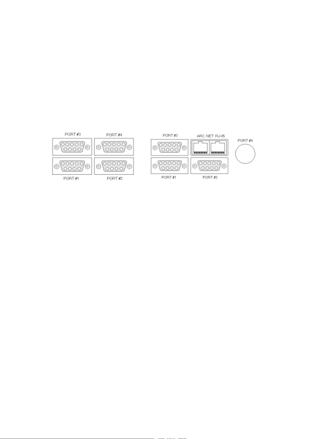
1-7. Interface
TYPE-I TYPE-II
Serial Port 1( on Main Board) RS232C ( 9 pin D-SUB)
PC / Barcode Scanner/ Slip Printer/ Modem
Serial Port 2( on Main Board) RS485( 9 pin D-SUB)
(available to change to RS232C by jumper modification)
I.R.C network
Serial Port 3( on Option Board) RS232C (9 pin D-SUB)
PC / Barcode Scanner + Ext. Display / Slip Printer
Serial Port 4( on Option Board)
Type-I RS232C(9pin D-SUB)
Type-II RS232C(DIN connector)
ARC. Net(RJ45) only on Option Board-TypeII
1-8. Optional Peripheral Device
Slip Printer EPSON TM295
Barcode Scanner
Kitchen Printer
Kitchen Printer Control Box( 4 suitable Terminal Printer Connection are available )
External Display( for Customer)
Credit Card Reader(Extension)
Scale
1-9. Power Consumption AC120V 60Hz 48W(max.)
AC230V 50Hz 48W(max.)
2
2. How to Install Roll Paper
Head-up lever
Take-up reel
2-1 Specification of thermal roll paper
The loaded printer is thermal head printer. Please use following thermal roll paper to change.
TF50KS-E by Jujyo Seishi ( recommendation)
Size: 44.5mm(width) x φ83mm(max.)
2-2 Step of changing
1) Cut the end of the roll paper correctly.
2) Put on a roll paper correct way and insert paper to the printer.
If power is on and the head-up lever is down, paper is inserted automatically
after inserting to the internal sensor position.
1

2-3 How to removing paper after paper jamming
If paper jamming occurs, follow the procedure below.
Cover frame screw
Cover frame
Head-up lever
1) Remove the cover frame screw. Then open the cover frame.
2) Release the head-up lever.
3) Remove all jammed paper and paper chips.
4) Return the cover frame until touching the portion.
5) Fix it with the cover frame screw.
2-5 How to adjust paper near-end sensor
If you want to adjust the near-end sensor timing, follows the procedure below.
1) Loosen the adjustment screw.
2) Move up or down the frame corresponding measure scale.
2

3. How To Change The Memory Back-Up Battery
3-1 How to change the memory back-up battery.
When needing to change the memory back-up battery, follow the procedure below.
1)Remove the printer cover from the cabinet.
2)Open the upper case by removing three screws which fix it.
3)Remove the battery from the holder by hand.
The supper capacitor installed on the main board will keep memory
for few minutes during change it.
Please use new battery as same as original type(IVR2430)
We can’t guarantee if you use any other kind of battery to change.
1

4. Operation for Maintenance
4-1 System Reset
This operation should be done immediately after changing program E-PROM or
repairing. All programmed data and report data will be kept after the system
reset operation.
DEPRESS
POWER OFF ‑‑‑‑> ‑‑‑‑‑‑‑> [RF] ‑‑‑‑‑‑‑> POWER ON
[JF]
P2 position [VOID]
4-2 Cancel password of the control lock mode
Even if P2 or P1 mode password is programmed, you can cancel it by a special
password “2001”. This password is also effective when losing original password.
4-3 Display Program version
Select "VERSION No. DISPLAY" in P2 mode main menu and press [CASH] key.
VERSION No.xxxx
Current ROM version is indicated to the last line.
4-4 ALL RAM Memory Clear
This operation should be done immediately after changing program E-PROM
version and install the extension memory board.
OPERATION SEQUENCE
SELECT PROGRAM ITEM
DETAIL SLIP FORMAT
VERSION NO. DISPLAY
RAM CLEAR OPERATION
Select "RAM CLEAR OPERATION" in P2 mode main menu and press [CASH] key.
Select “All RAM CLEAR”and then press [CASH] key. If you want to exit, press [TOTAL] key.
1
RAM CLEAR OPERATION
ENTER PASSWORD
0
Enter system password (2001) and enter [CASH] key.
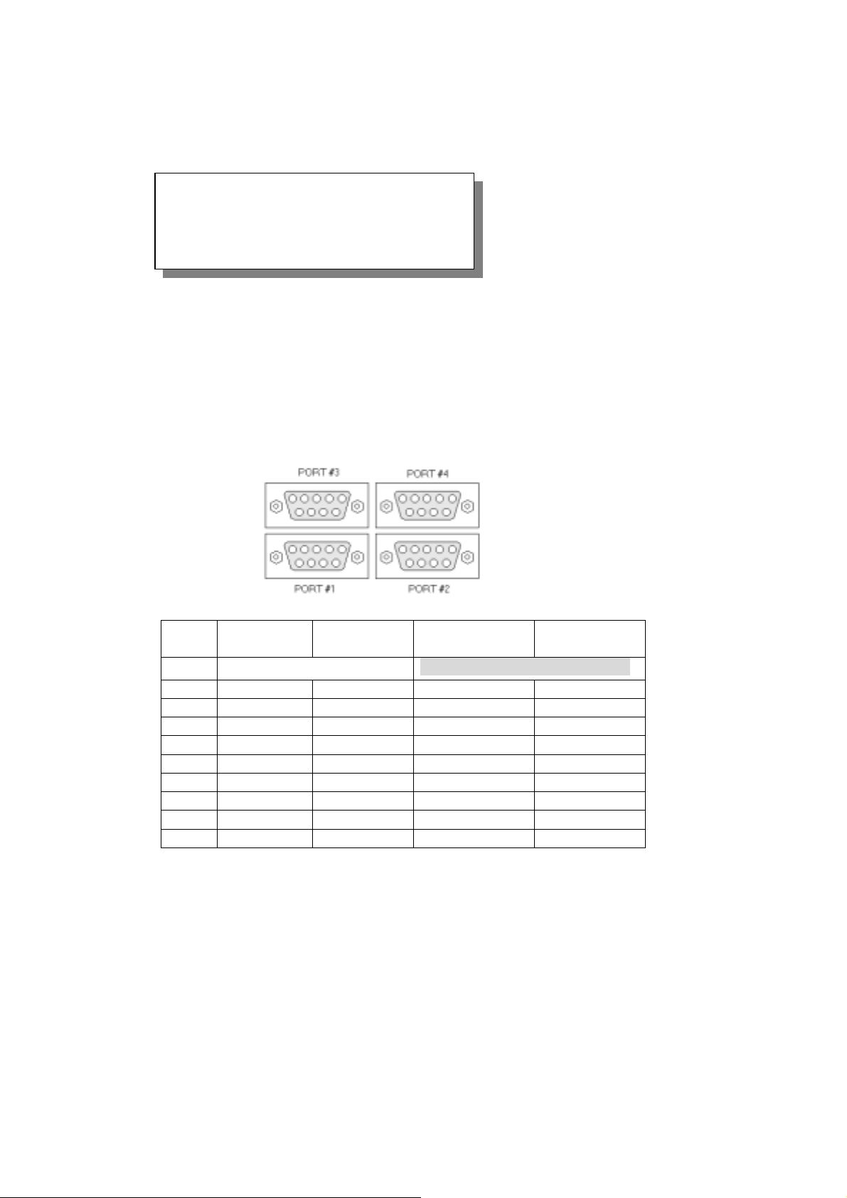
4-5 Communication Port Loop Back Test
This test checks if serial port circuit works by loop back sequence.
Before starting this test, loop‑back connector should be connected to a D‑SUB connector without
port #2 that you want to check. This loop‑back connector should be shorted 2nd pin and 3rd,4th
and 8th .
PIN Assignment
PIN# #1 PORTA #2 PORT B #3 PORT C #4 PORT D
with IF. cable
On the Main Board Extension Memory I/O Borad
1 NC NC NC NC
2 RXD (RXD) RXD RXD
3 TXD (TXD) TXD TXD
4 DTR (DTR) DTR DTR
5 SG SG SG SG
6 DSR TX- NC NC
7 RTS TX+ NC NC
8 CTS (CTS) CTS CTS
9 +5V +5V (+5V) (+5V)
2

Connect the LOOP‑BACK connector to the port that you want to check.
Select "SYSTEM TEST" in P2 mode main menu and press [CASH] key.
SELECT PROGRAM ITEM
RAM CLEAR OPERATION
IRC RAM COPY
SYSTEM TEST
Enter target port number and press [CASH] key.
SYSTEM TEST
ENTER TEST PORT No.
0
The loop-back test will be done and results will be printed on the receipt.
4-6 E-PROM CHECK-SUM Printing
You can print the check-sum value of the main E-PROM by following operation.
Turn to the S-position by using the S-key.
Enter system PASSWORD (2001) and enter [CASH] key.
3

5 LOGIC CIRCUIT
CN10, CN11
CN1
CN3
CN4
Auto Cutter
Thermal Head
Feed Motor J
Feed Motor R
CN2
MT245 Thermal
Printer
Fiscal Memory
CN12
CN9
CN8
Drawer A
Drawer B
Line Noise
Filter Board
Front Display Board
VFD. Back Display
Control
Lock
Cashier
Key
CN7 CN4
CN9,CN10
KEY Board
Unit
CN5
CN6
LCD 20 x 4 Display Module
CN11 CN12
Main Board Unit
Paper Near‑End R
Paper Near‑End J
CN15
CN14
CN16
Connection Diagram
CN5
CN6
RS485 for I.R.C.
RS232C
Extension
Memory I/O
Board
CN7
CN1
CN5
CN5
RS232C
RS232C
POWER
TRANSFORMER
5-1 Connection Diagram
1
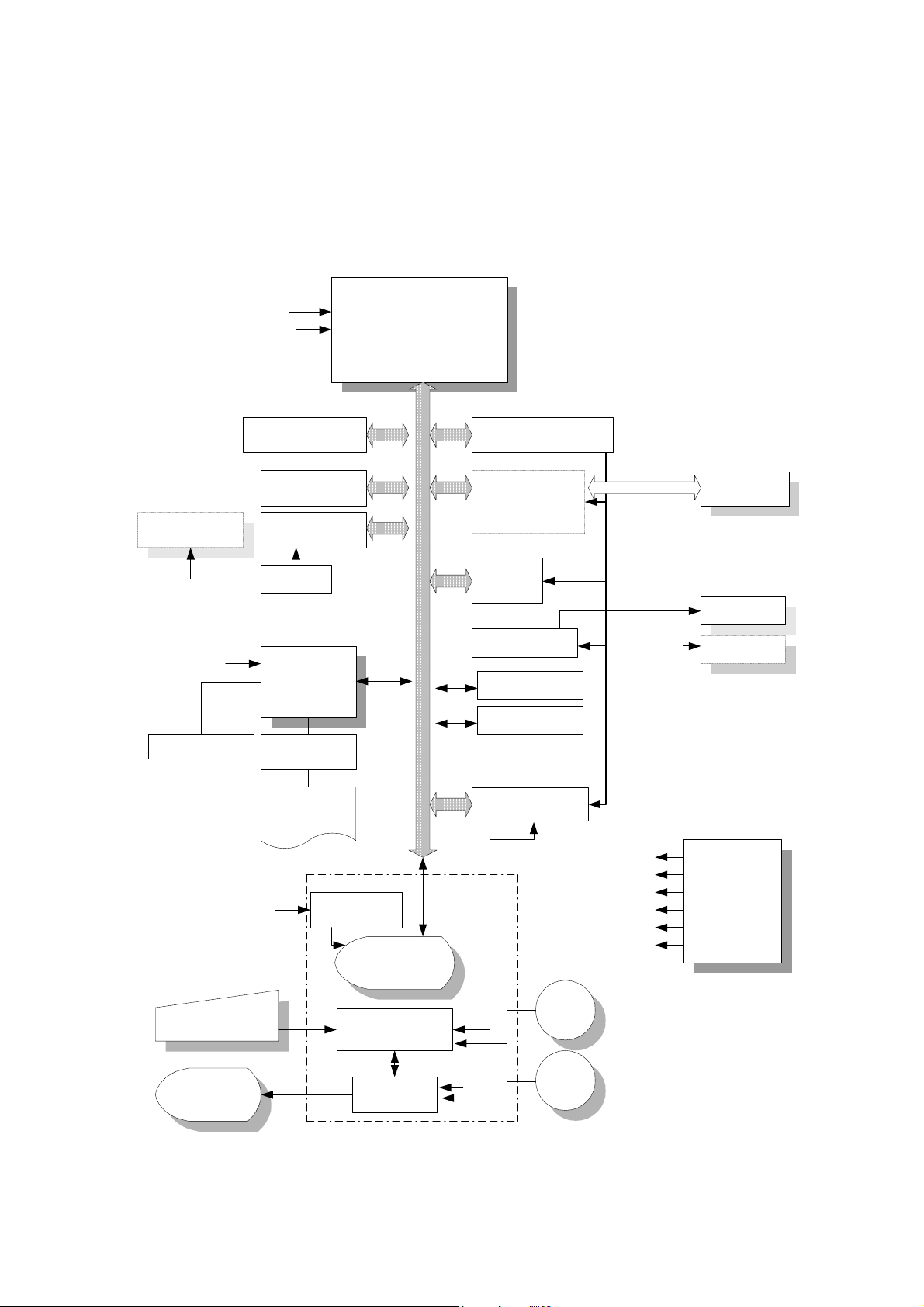
5-2 Block Diagram
CPU HD64180Z
ROM 256K bytes
27C2001
RAM 512K bytes
TC54001CF
RAM 512K bytes
Drawer Drive &
Sensor Circuit
Back‑Up
Battery
Power Circuit
+24V,+5V,VFD
/RESET
/POWER FAIL
/RESET
/POWER FAIL
Real‑Time
Clock
RTC72423
Printer
Controller
M37732SAFP
ROM 32K bytes
Printer Driver
Circuit
MT245
Thermal R/J
Printer
4x20 LCD DOT
Display Module
VFD Numeric
Back Display
SCANNING
Multiplex
Circuit
DC/DC for
Back‑Light
VFD Driver
uPA80GR x 3
Control
Lock
Chashier
Key
Keyboard Unit
+24V
Vf
Vgrid
Fiscal Memory
Control Circuit
82C55 & HC273
Fiscal Memory
27C1001
I/O ADDRESS
DECODER GAL
MEMORY ADDRESS
DECODER GAL
Sync
Serial
RS485 Driver
MAX491
RS232C Driver
MAX238
PORT0
PORT1
KEY & DISPLAY
SCANNING Circuit
Sync.
Port
Drawer A
Drawer B
Vf
Vgrid
+24V
VCC
/RESET
/POWER FAIL
/RESET
2

5-3 Primary Power Circuit
1)Filter Circuit
AC power is supplied to the transformer through a fuse and the filter circuit.
The filter circuit is constructed three capacitors and a choke coil as a common mode
filter.
2)AC Power Transformer
This power transformer has two primary taps ( brown and red). The brown is for 115V
and red is for 230V range. By both taps,32V(AC) voltage is output to the secondary
side.
3

5-4 Power Circuit
5-4-1 VP(+24V) Generation Circuit
The AC power from the secondary of transformer undergoes full wave rectification by
diode bridge DB1 and smoothed by capacitor C4. After smoothing DC power is
supplied to DCDC converter U1(STK733). The main power VP is supplied to each
part after regulating to 24V by this DCDC converter.
5-4-2 VCC, Vf ,Vgrid Generation Circuit
The regulated VP is supplied to self-oscillator circuit made up Q1,Q2,R23,C23 and T1.
VF1&2 for heating filament of VFD,-Vgd(-29V) for grid of VFD and VCC(+5V) are
generated from the VP by this DCDC converter circuit.
4
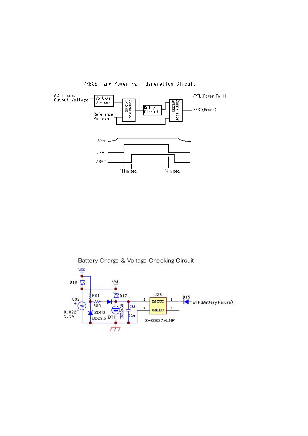
5-5 Power Failure & Reset Signal Generation Circuit
Secondary voltage of the power transformer which is rectified by D1 and D2 is
supplied to the comparator U3 as a checking voltage after dividing properly by
R1,R2,R7,R8 and R6. This voltage is compared with reference voltage which
generated by ZD4 and power failure signal /PFL is generated. This /PFL signal
generates reset signal /RST after coming out of the delay circuit and next comparator.
5-6 Battery Charge & Voltage Checking Circuit
The VCC, which is adjusted to 3.6V by the ZD10 supplies to the battery BT1 during
power on. The VCC also charges the supper capacitor C92. When turning power off,
the battery voltage 3.0V is supplied to back-up C-MOS RAM and real-time clock IC .
And this battery voltage is always checked if voltage is less than 2.7V by a voltage
checking IC U28. If the battery voltage is less than 2.7V, the BTF signal will be
active on to inform battery voltage error.
5

5-7 Memory Selection Circuit
Address decode circuit of main memory is constituted with a programmable array
logic IC U24. This IC makes five kinds of selection signals from address
lines(A15-A19) and memory enable signal /ME.
Device Purpose of using
/M0 U25 M27C1001 Used for 512K bytes Program Area
/M1 U30 TC554001 Used for reading of 512K bytes data area
/M2 U30 TC554001 Use for writing of 512K bytes data area
/M2 EXTERNAL RAM Used for reading of 256K bytes data area
/M3 External RAM Use for writing of 256K bytes data area
6

5-8 I/O Selection Circuit
Address decode circuit of I/O is constituted with a programmable array logic IC U10.
This IC makes ten kinds of selection signals from address lines(A12-A15) and I/O
enable signal /IOE.
Device Purpose of using
/IO0 U29 Real-time Clock IC Used for selecting real-time clock IC.
IO1 U8 Latch IC HC374 Used for making segment data of VFD.
IO2 U16 Latch IC HC374 Use for making scanning selection.
IO3 U9 Latch IC HC374 Used for making LCD control signal.
/IO4 Not used
/IO5 U18A Buffer IC HC240 Used for making credit card reader interface
signal.
/IO6 U13 PPI MSM82C55 Used for making data and address bus line
of fiscal memory.
/IO7 U7 Buffer IC HC244 Used for reading key-scanning(R0-R7)
/IO8R U14B Buffer IC HC244 Used for reading printer status information.
/IO8W U23 Latch IC HC174 Used for making DTR0,DTR1 and sub
memory bank signal MBNK.
/IO9R U17A Buffer IC HC244 Used for reading status of connection with
fiscal memory, battery voltage and paper
near end.
/IO9W U15 Latch IC HC273 Used for making fiscal memory control
signal.
7

5-9 Real-Time Clock Circuit
The RTC72423 is a bus-connection real-time clock IC built-in crystal oscillator.
Date and time data is read or written from the CPU by 4bits data line,
4bits address lines and control lines.
5-10 Buzzer Circuit
Four gates in U1 and R1,R2 and C2 constitute a self-oscillation circuit. When BUZ
signal from the main board is on, the VP synchronizes with this pulse and is supplied
to the speaker BZ1 by transistor Q1.
8
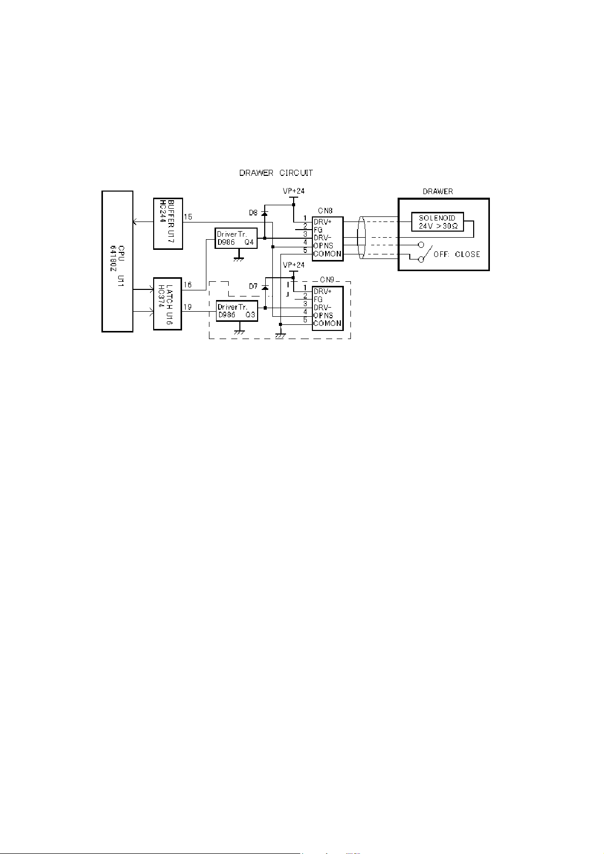
5-11 Drawer Circuit
The driving pulse signal, which is made by latch IC U16, drives a transistor D986
and drawer solenoid will be driven. The status of the drawer open sensor is read to
the main CPU through the buffer IC U17.
9
Table of contents
Other BMC Cash Register manuals


