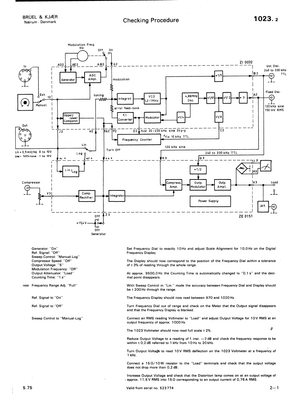
1023.1
Technical Description
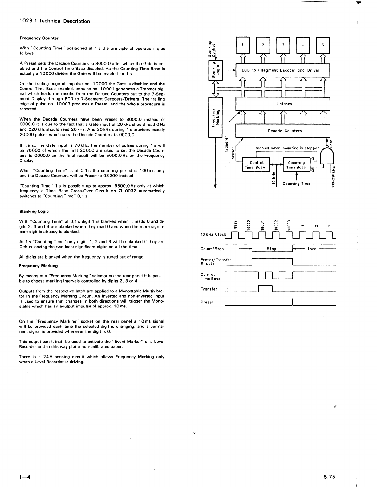
Frequency Counter
With
"Counting
Time"
positioned at 1 s
the
principle
of
operation is as
follows:
A Preset sets the Decade Counters
to
8000,0
after
which
the Gate is en-
abled and the Control Time Base disabled.
As
the
Counting Time Base is
actually a
10000
divider the Gate
will
be enabled for 1 s.
On
the trailing edge of impulse no.
10000
the Gate is disabled and
the
Control Time Base enabled. Impulse no.
10001
generates a Transfer sig-
nal
which
leads
the
results
from
the
Decade Counters
out
to
the
7-Seg-
ment Display
through
BCD
to
7-Segment
Decoders/Drivers.
The
trailing
edge
of
pulse no.
10003
produces a Preset, and
the
whole
procedure is
repeated.
When
the Decade Counters have been Preset
to
8000,0
instead
of
0000,0
it
is due
to
the
fact
that
a Gate
input
of
20
kHz should read 0
Hz
and
220
kHz
should
read
20
kHz.
And
20
kHz
during
1 s provides exactly
20000
pulses
which
sets the Decade Counters
to
0000,0.
If
f. inst.
the
Gate
input
is
70
kHz,
the
number
of pulses
during
1
swill
be
70000
of
which
the
first
20000
are used
to
set
the
Decade Coun-
ters
to
0000,0
so
the
final
result
will
be
5000,0
Hz
on
the
Frequency
Display.
When
"Counting
Time"
is
at
0,1 s the counting period is
100
ms only
and the Decade Counters
will
be Preset
to
98000
instead.
"Counting
Time"
1 s is possible up
to
approx.
9500,0
Hz
only at
which
frequency a
Time
Base Cross-Over
Circuit
on
ZI
0032
automatically
switches to
"Counting
Time"
0,1 s.
Blanking
Logic
With
"Counting
Time"
at 0,1 s digit 1 is blanked
when
it
reads 0 and di-
gits 2, 3 and 4 are blanked
when
they
read 0 and
when
the more signifi-
cant digit is already is blanked.
At
1 s
"Counting
Time"
only
digits
1, 2 and 3
will
be blanked
if
they
are
o
thus
leaving the
two
least
significant
digits on all
the
time.
All
digits are blanked
when
the frequency is
tuned
out
of range.
Frequency Marking
By means of a
"Frequency
Marking"
selector on the rear panel
it
is possi-
ble to choose marking intervals controlled by
digits
2,
3
or
4.
Outputs from the respective latch are applied to a
Monostable
Multivibra-
tor in the Frequency
Marking
Circuit.
An
inverted and
non-inverted
input
is used to ensure
that
changes
in
both directions
will
trigger
the
Mono-
stable
which
has an
aoutput
impulse of approx.
10
ms.
On the "Frequency
Marking"
socket on the rear panel a
10
ms signal
will
be provided each
time
the
selected
digit
is changing, and a perma-
nent
signal is provided
whenever
the
digit
is
O.
This
output
can f. inst. be used
to
activate
the
"Event
Marker"
of
a Level
Recorder and in
this
way
plot a non-calibrated paper.
There is a
24
V sensing
circuit
which
allows
Frequency
Marking
only
when
a Level Recorder is driving.
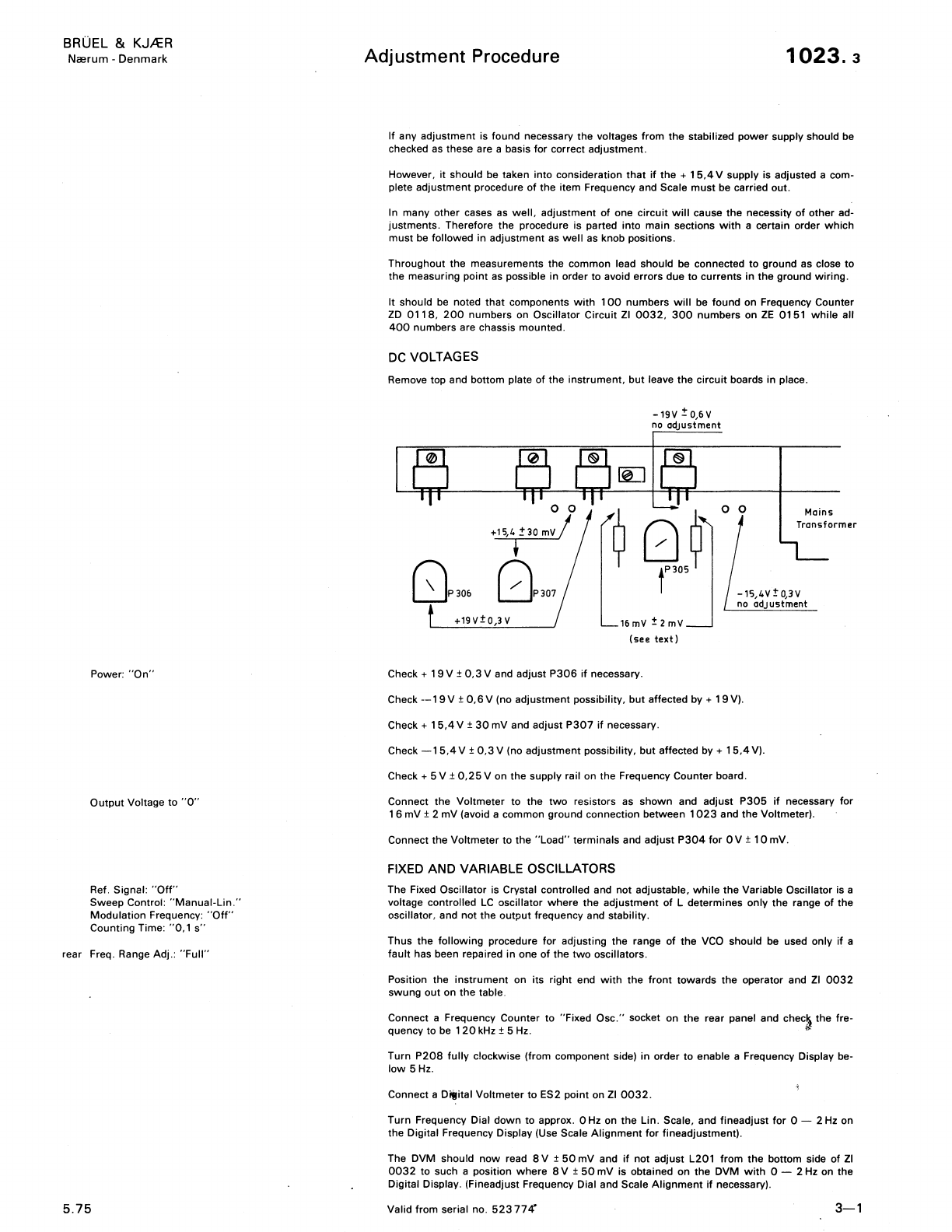
1-4
~01
c: c:
.,.-
".:.:
er'-
.,
0
'-~
"-
Count/Stop
Preset/
Transfer
Enoble
Control
Time Bose
Counting Time
=:J'--
___
S_t_o-'-p
__
--'F
Isec.
---
LJLnJ
Transfer
______
~r-l~
____________
__
Preset
5.75
T
,