BRUEL & KJA:R
Ncerum
Denmark
Power
Supply
FilTER:
"linear"
INTERNAl BATIERY
Frequency
Tuning
Volta
ge
FILTER:
"Linear"
FREQUENCY TUNING
"r
SWEEP
CONTROl
"Manual"
DC-Off-set
Adjustment
FILTER
"23%"
FREQUENCY TUNING
"20"
SWEEP
CONTROl
"Manual"
Adjustment Procedure
1621.2
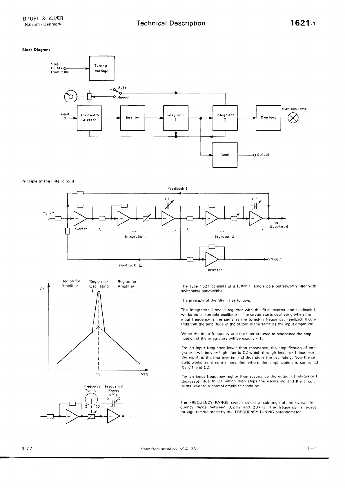
Check the
following
voltages and adjust if necessary. +
12V
±0,3V
DC.
(P113)
+
lOV
±O,l
V DC.
(Pl11)
~10V
,,0,1
V DC.
(P112)
Remove
the
connection
between
P3 and
R26
on
lE
0161.
(Marked
'F'
on
the
P.
C board)
Adjust
the voltage on
the
slider
of
P3:
-1.20V
=
0,05
V
Reconnect P3 to
R26.
Check the voltage across
P120
FREQUENCY TUNING:
66
mV ± 2 mV
If necessary
adjust
P1O
Check if the voltages are
OV
0,2
mV
DC
between
ground
on
lE
0161
and
the
following
components (pin
2)
Component
V16 V15
V6
V12
If necessary ad]ust P4 P6 P9
P8
Amplitude
Controi
FilTER to
"Linear"
FREQUENCY RANGE
"2002K"
FREQUENCY TUNING:
"10"
MAX.
VOLTAGE:
"1
V"
SWEEP
CONTROl'
"Manual"
FILTER
to
..
3%"
FREQUENCY RANGE to
"2k-20k"
FilTER to
"Z3%"
Frequency
Control,
Manual
FilTER
"3%"
FREOUENCY RANGE
"ZO-200"
FREQUENCY TUNING
"2"
MAX.
VOLTAGE:
"1
V"
SWEEP CONTROL'
"Manual"
FREQUENCY TUNING to
"20"
FREQUENCY TUNING to
"2"
9.77
Check the voltage
between
pin 2 and 3 on
V17:
OV ±
0,2
mV.
If
necessary
ad]
ust P1.
Input
signal to
"Filter
Input";
1000
Hz
adjusted
for
1 V
deflection
on an electronic voltmeter
connected to
"Filter
Output"
Fine adJust FREQUENCY TUNING
for
maximum
output
voltage.
Deflection:
1 V ±
O,6dB.
If necessary adjust P
114.
(lG
0109)
C~ange
signal frequency to
10kHz
and check the
output
voltage
Deflection:l
V
0,6
dB.
If necessary
adjust
Pl15.
(ZG
0109)
For
the
positions
of
FREQUENCY RANGE
"0.2·Z",
"Z-20",
"ZO-200"
the tolerances are
±
O,6dB,
but
no adJustments.
Check as above.
Tolerance'
0,3
dB
0,6
dB
in"2
k
20
k"range
Input
signal:
20
Hz
0,01
Hz
• 1 V
Fine
adjust
FREQUENCY TUNING
for
maximum
output,
voltage
loosen
the
knob and
turn
the
pointer
to position 2.
Change signal frequency to
200
Hz
0,1
Hz
Adjust
P5
{ZE
0161)
for max.
output
voltage
Repeat
the
above adJustments
as
they
influence
e8ch
olhers
Check the frequency
for
the
other
positions
of
FREOUENCY
RAt'<GE.
Tolerance: ± 1%
In
the
rango"Zk-20k'
the frequency can be
adjusled
by
C
118.
(ZG
0109).
Valid from serial no.
6941Z6
-
2-1