CONTENTS
CE-6800 Page
1. SPECIFICATIONS........................................................................................ 1
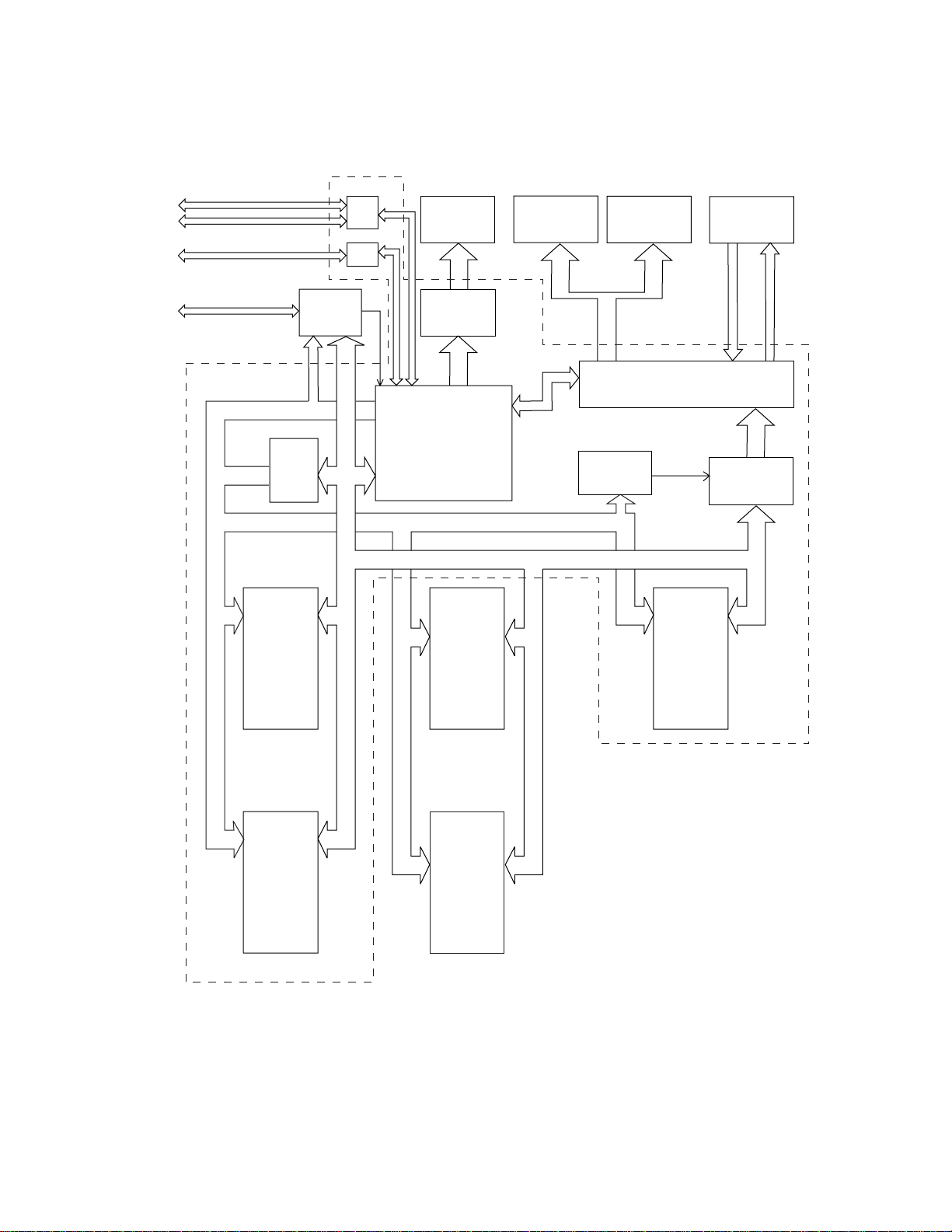
2. BLOCK DIAGRAM....................................................................................... 3
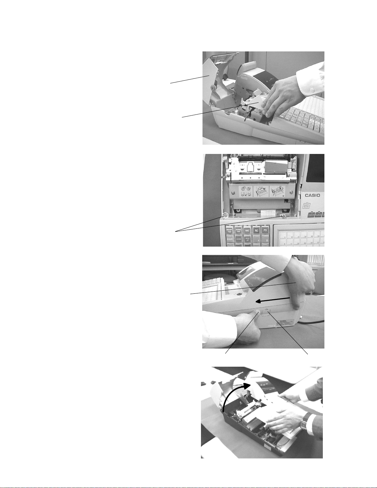
3. TO OPEN THE UPPER CASE ..................................................................... 5
4. CIRCUIT EXPLANATION ............................................................................ 7
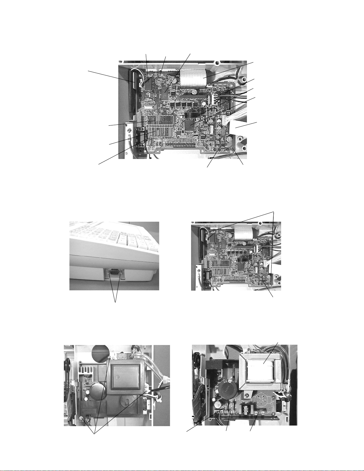
4-1. Power supply circuit ................................................................................................. 7
4-2. Reset and power down circuit.................................................................................. 8
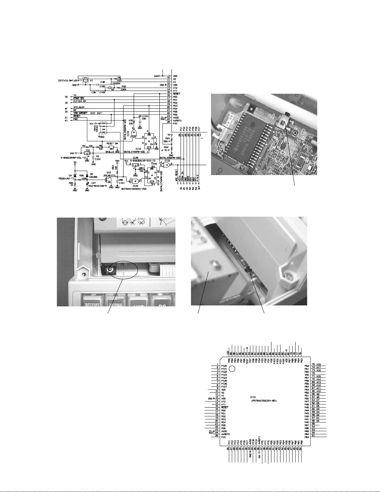
4-3. CPU description......................................................................................................... 8
4-4. Momory chip selection circuit................................................................................ 11
4-5. Flash ROM1 address circuit ................................................................................... 12
4-6. Memory map ............................................................................................................ 12
4-7. Printer drive circuit.................................................................................................. 13
4-8. RS232C port COM1 circuit...................................................................................... 14
4-9. RS232C port COM2 and COM3 circuit ................................................................... 15
4-10. To mount optional circuit ....................................................................................... 16
5. DIAGNOSTIC OPERATION....................................................................... 17
5-1. To start the diagnostic program ............................................................................ 17
5-2. Check item ............................................................................................................... 17
5-3. Operation of each test............................................................................................. 17
5-4. Switch status test .................................................................................................... 18
5-5. Individual function test ........................................................................................... 19
5-6. To exit the diagnostic mode ................................................................................... 27
6. IC DATA ..................................................................................................... 28
7. PCB LAYOUT ............................................................................................ 38
8. CIRCUIT DIAGRAM ................................................................................... 40
9. PARTS LIST............................................................................................... 56