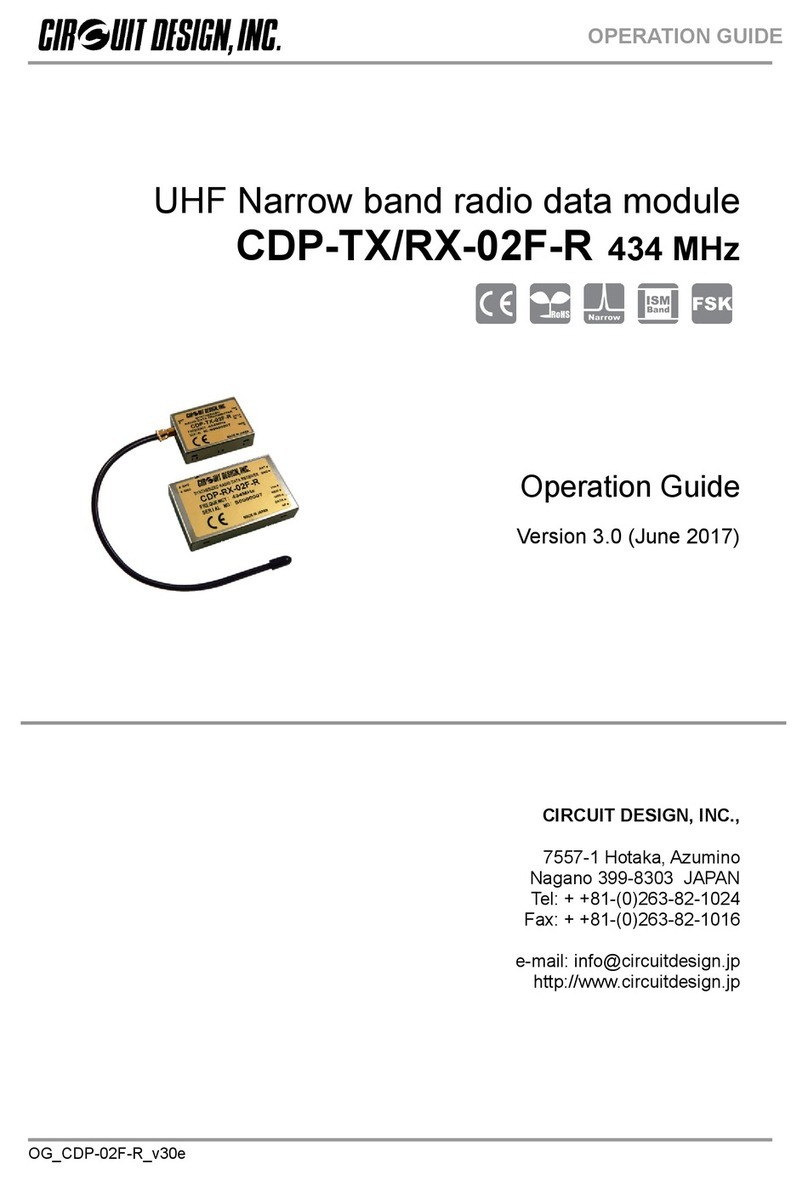
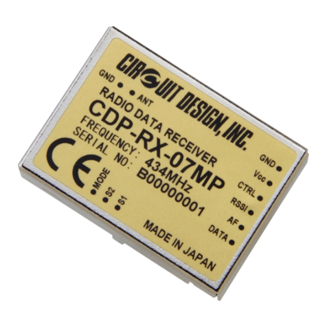
CIRCUIT DESIGN CDP-02N Series User manual

7557-1 Hotaka,Hotaka-machi,Minamiazumi,Nagano 399-8303,Japan
Tel:+81-263-82-1024 Fax:+81+263-82-1016
http://www.circuitdesign.co.jp/
CDP-TX/RX-02NDS ver1.0
CIRCUIT DESIGN, INC. International Business Division
Feature
Application
Remote control systems
Security systems
Alarms
Telemetry systems
European EN300-220 compliance
32 frequency synthesized RF channels
5mW/10mW selectable
Low voltage operation
High sensitivity 300m range
FM narrow band modulation and
high frequency stability
Common Item
Communication form
Oscillation system
Frequency range
Number of RF channels
Channel step
Frequency stability
Baud rate
Operating temp. range
Transmitter type
RF output power
Transmitter start up time
Modulation
Data input level
Input signal
Deviation
Spurious emission
Adjacent channel power
Supply voltage
Supply current
Dimensions
Weight
Receiver type
Sensitivity
Selectivity
Demodulation
Distortion
S/N ratio
Data output
Supply Voltage
Supply current
Dimensions
Weight
Specification
One way
PLL controlled VCO
433.875MHz to 434.650MHz
32 ch
25kHz
+/-2.5kHz (-10 to +55 degree C)
300 to 4800bps
-10 - +60 degree C
PLL synthesizer
10mW/5mW
80msec
FM Narrow
2.2 - 12V
Digital
2.0kHz
<-60dBm (< 862MHz) , <-46dBm (>= 862MHz)
<200nW
2.4 - 12V DC
30mA (typ)
36 X 26 X 10 mm
12.5g
Double Superheterodyne PLL synthesizer
-120dBm (12dB/SINAD at CCITT filter)
+/-7.5kHz at -6dB point
FM Narrow
<3% at 1kHz
35dB overall (AF out)
Digital
3.6 to 12V DC
26mA (typ)
50 X 30 X 9mm
19g
UHF Narrow Band Multi Channel Transmitter/Receiver
CDP-TX-02N/ CDP-RX-02N
The unique and compact CDP-02N is a frequency selectable radio data module for 434MHz UHF band. Both
CDP-TX-02N (transmitter) and CDP-RX-02N (receiver) are equipped by frequency synthesizer system with
microprocessor. Frequency range of CDP-02N is from 433.875MHz to 434.650MHz in 32 channels which are
selectable by the use of an onboard 4 bits switch.
Small size, low voltage operation and frequency selectability of CDP-02N make it ideal for various applications in
sites where many radio transmitters are operated.
CDP-TX-02N
(Transmitter)
CDP-RX-02N
(Receiver)
Specifications are subject to change without prior notice

CIRCUIT DESIGN, INC.
CDP-02N UHF Synthesized Radio Data Module Operation Guide 1
C
CD
DP
P-
-0
02
2N
N
CDP-TX-02N& CDP-RX-02N (433MHz)
CDP-TX-02AN& CDP-RX-02AN (458MHz)
UHF FM-NARROW BAND SYNTHESIZED RADIO DATA MODULE
Operation Guide
Version 1.4 (July, 2002)
CIRCUIT DESIGN, INC.,
International Business Division
7557-1 Hotaka, Hotaka-machi, Minamiazumi, Nagano 399-8303. JAPAN
Tel: + +(0263)-82-1024 Fax: + +(0263)-82-1016

CIRCUIT DESIGN, INC.
CDP-02N UHF Synthesized Radio Data Module Operation Guide 2
CONTENTS
GENERAL DESCRIPTION & FEATURES ................................ 3
CDP-TX-02N transmitter module ....................................... 4
CDP-RX-02N receiver module ........................................... 4
OPERATION INSTRUCTIONS ................................................... 6
Supply voltage ..................................................................... 6
Data input ............................................................................ 6
Data format .......................................................................... 7
Channel and frequency setting ............................................ 7
Outputs ................................................................................. 8
Test Set ECB-03 and DCB-03 .............................................. 8
Antennas .............................................................................. 8
Start up.................................................................................. 9
SPECIFICATIONS...................................................................... 10
CHANNEL AND FREQUENCY SETTING .............................. 11
BLOCK DIAGRAM ................................................................... 13
DIMENSIONS ............................................................................ 14
DATA .......................................................................................... 15
IMPORTANT NOTICE .............................................................. 16
CAUTION & WARNING DIMENSIONS ................................. 16

CIRCUIT DESIGN, INC.
CDP-02N UHF Synthesized Radio Data Module Operation Guide 3
GENERAL DESCRIPTION & FEATURES
Features
• Compatible with European EN 300 220 standard
• Very small compact integrated device with PLL synthesizer and micro controller
• Frequency selection free in 32 channels for 433MHz, 11 channels for 458MHz
• New integrated UHF filter technology
• 5mW/10mW selectable
Applications
•Radio remote control cranes and machines
•Radio remote control for garage door controls
•Security systems
•Room surveillance
•Theft protection
•Telemetry systems
General description
The CDP-02N consists of CDP-TX-02N (CDP-TX-02AN) transmitter and CDP-RX-02N
(CDP-RX-02AN) receiver. It is suitable for various application fields such as wireless data
communication, remote control, telemetry or wireless security systems. It is easy to use and
integrate into application systems.
The CDP-02N is equipped with a frequency synthesizer system with micro controller. The
frequency range of the CDP-02N (EU type) is from 433.875MHz to 434.650MHz in 32
channels which are selectable by use of a 4 bits switch, and a jumper on the PCB for 2 groups
of 16 channels. The frequency range of the CDP-02AN (UK type) is from 458.525MHz to
458.775MHz in 11 channels, which are selectable with a 4 bits switch.
The compact size, low operation voltage and frequency selectability of the CDP-02N make it
ideal for various applications where its interference rejection and practical distance range is
far better than similar RF modules based on wide band SAW-resonator frequency generators.
Standard RS232 serial data and other digital data (TTL level), such as pulse width modulation
signals and signals from standard encoder-decoder circuits of the given AF bandwidth, can be
transmitted.

CIRCUIT DESIGN, INC.
CDP-02N UHF Synthesized Radio Data Module Operation Guide 4
CDP-TX-02N transmitter module
The CDP-TX-02N (CDP-TX-02AN) is a UHF FM-narrow band transmitter with PLL
synthesizer and micro controller for high frequency stability and channel selectability. Modern
SMT technology enable its small size - much smaller than a match box.
The narrow band FM modulation (direct FSK) allows efficient use of the available RF
spectrum. Different modules can operate in a 25 KHz channel spacing scheme unlike SAW
resonator transmitters which use a very broad band of the frequency spectrum. 32 channels
can be easily selected by use of the chip mounted 4 bits switch and a PCB jumper. Please refer
to the section on channel plan and frequency setting for details.
The CDP-TX-02N (CDP-TX-02AN) can transmit any 5 Volt digital input data in the specified
frequency range. Analog data is digitized by the internal comparator.
In about 80mS (90msec for 458MHz) after the transmitter is connected to a power source,
PLL is locked and data can be transmitted without further control or synchronization.
The transmission is physically done by a flexible Lambda/4 antenna connected to the module.
The amount of radiated power and the surrounding of the antenna influences directional
behavior. Installation in a bigger metal housing with ground connected to the transmitter
module housing and the transmitter antenna placed in an upright position outside the metal
housing will reduce the antenna impedance and increase the radiated power. For best
performance in a user system general rules of radio frequency technology should be taken into
consideration.
The same considerations should also be applied to the receiver.
CDP-RX-02N receiver module
The CDP-RX-02N (CDP-RX-02AN) is a UHF receiver for FM-narrow band modulated
signals.
The receiver design is based on the double Super-heterodyne principle with PLL synthesize
system and micro controller enabling high signal sensitivity, high selectivity, and high
frequency stability not achieved by simple SAW resonator receivers or other low cost designs.
The channel frequency can be easily selected to match the frequency of the transmitter. The
method of frequency selection is the same as CDP-TX-02N (CDP-TX-02AN).
Extensive filtering by an integrated unique SAW filter element enables operation in hazardous
areas where interference may be expected. Steadily increasing use of the available frequency
spectrum demands the application of narrow band systems for maximum operation reliability
and consideration for other users of the ISM band.
The CDP-RX-02N (CDP-RX-02AN) receiver module is designed to match the CDP-TX-02N
(CDP-TX-02AN) transmitter module, though signals from other FM-narrow band transmitters
can be received as well.
The CDP-RX-02N (CDP-RX-02AN) is designed for mounting on a PCB. A simple wire can
be soldered to the antenna input or the antenna can be printed on the PC board. Better
performance is attained with commercial antennas for the 433MHz (458MHz) ISM band.
The receiver modules have two different outputs and an RSSI field power output which
CIRCUIT DESIGN, INC.
CDP-02N UHF Synthesized Radio Data Module Operation Guide 5
indicates the power of the incoming RF signal.
The AF output is the analog output from the FM detector circuit. Voltage level, DC-offset and
AF noise depend directly on the receiver-input signal. This output can be connected to an
MSK decoder circuit if a transmitter with additional MSK encoder is used*1. For simple FSK
modulation of digital data, the DATA OUT terminal can be used. It contains a band-pass filter
and comparator with digital output (open collector).
To achieve the high signal sensitivity and short receiver response time no internal muting is
applied. Valid data signals can be detected by utilizing the RSSI output.
*1 The data input of the CDP-TX-02N(CDP-TX-02AN) is for digital signal. In case the output of the
MSK encoder is inputted to the DATA IN of the CDP-TX-02N(CDP-TX02AN), please make sure to
input the digitatized signal to the DATAIN by saturating the signal beforehand.

CIRCUIT DESIGN, INC.
CDP-02N UHF Synthesized Radio Data Module Operation Guide 6
OPERATION INSTRUCTIONS
Please read these instructions before you start using the CDP-02N.
The CDP-02N is designed as a module which will be integrated into a user system. It is not a
ready-made product for private users. It can be regarded more like a special component for
part of an electronic system. The user needs basic knowledge about electronics. Special
knowledge about RF technology is helpful, but the most difficult parts are integrated into the
modules to enable easy operation. Some additional information is given here:
Supply voltage:
The transmitter and receiver module contain a voltage regulator to guarantee stable
performance in the given range of supply voltage.
The design was made for operation with a battery or regulated power source. If the battery
voltage drops below the minimum voltage given in the technical specifications, the transmitter
output power will drop and the RF oscillator will stop operation. No data can be transmitted in
this case. The receiver will continue to work down to a certain voltage but the performance
will deteriorate.
If the voltage connected to the Vcc (+) and Ground (-) terminal is above the maximum voltage
given in the technical specification the internal voltage regulator will be permanently
damaged. The result is an internal short-circuit or disconnection.
To enable a low minimum voltage no internal circuit is used to prevent damage by incorrect
polarity. If the transmitter is connected incorrectly, it will be permanently damaged. If a higher
supply voltage is available then a simple diode can be inserted in the connection line to the
Vcc terminal to prevent damage by incorrect polarity. The diode must be rated for the
maximum supply current detailed in the technical specifications.
Modules which have been connected to improper voltage sources should be returned to the
dealer for inspection.
Data input:
The data input terminal is connected to a digital transistor compatible input. Data
sources of high impedance can be used is acceptable.
The voltage of the data signal should be between 0V (Ground level) and Vcc. Because of the
internal voltage regulator, it is recommended that the data high level be limited to 5 Volts.
The data can be an analog or digital signal. Analog signals will be converted to a digital 1 or 0
inside the transmitter.
It is not necessary to synchronize the data signal of the transmitter, but the data signal should
be fed to the transmitter 80ms after the transmitter power on.

CIRCUIT DESIGN, INC.
CDP-02N UHF Synthesized Radio Data Module Operation Guide 7
Data format:
The digital data fed to the transmitter is passed through an internal low-pass filter to limit the
bandwidth of the digital data. This is needed for an efficient use of the available RF spectrum.
At the receiver, a band-pass filter is used to recover the data signal from noise. Together the
transmittable signal bandwidth is approximately 150 Hz to 2400 Hz. At the receiver, the signal
is converted back into a digital signal for compatibility with succeeding digital systems. The
type of digital data signals transmittable is limited by the bandwidth of the system.
DC signal or long intervals of HIGH or LOW bits should be avoided. Succeeding bits can be
distorted in their bit length. If the sequence of HIGH or LOW bits is too long it is possible that
the logic level of the data output will be changed.
The best countermeasure is to use a digital encoding scheme, which guarantees that no low
frequency components are included in the data signal. This can be achieved, for example, with
the "Manchester" encoding. A digital 1 is coded in a sequence of 10 and a digital 0 is encoded
into a sequence of 01. In most cases it is also sufficient to transmit serial data by using start
and stop bits of different logical level as can be done with the RS232 format. Each transmitted
byte will be preceded by a 0 bit and succeeded by a 1 bit.
The CDP-02N was tested with a number of standard encoder-decoder IC's for simple remote
controls. For data speeds in the 300 to 4800 Baud range no trouble should occur.
Because of the wide variety of data formats, data speeds and digital modulations techniques, it
is best to set-up a 'worst case' scenario and test the data transmission before the CDP-02N is
used in a practical application.
Further advice can be given if the precise format of the data and system requirement is
notified to the dealer or directly to Circuit Design, Inc. Your inquiries and comments are
welcome and will also help other users.
Channel and Frequency Setting:
EU Type
By use of chip mounted 4 bits switch and a jumper on the PCB, 32 channels can be easily
selected.
The 32 channels are divided to 2 groups: group A and group B. Each group of channel can be
selected by solder the jumper ON or OFF. The jumper ON is the state of group A. The jumper
OFF is the state of group B. There are 16 channels in each group and can be selected by the 4
bits switch easily.
Before shipment all the modules are set to the group B and all the 4 bits of switch are set to
the state of OFF. (434.65 MHz)
UK Type
All the 11 channels can be easily selected by the 4 bits switch on PCB. Please refer to the
CHANNEL AND FREQUENCY SETTING for channel selection.

CIRCUIT DESIGN, INC.
CDP-02N UHF Synthesized Radio Data Module Operation Guide 8
Outputs:
At the receiver side 3 output signals are available.
AF is the direct analog output of the FM receiver.
This signal can be used for checking the receiver and in cases where signals with additional
analog modulation are to be received. For example, it can be connected to an MSK decoder.
The DATA output is a digital open collector output. An internal 10KOhm pull-up resistor is
applied to enable direct connection to CMOS compatible circuits. For other applications an
additional external pull-up resistor should be used.
The receiver has no internal mute circuit to avoid delays and achieve maximum sensitivity.
The AF and DATA output will show noise on the output when no signal is received.
The third output is called RSSI. It is an indicator of the received signal strength. It can be used
to drive an external mute circuit.
Test Set ECB-03 and DCB-03
The Test Set ECB-03 and DCB-03 were developed to demonstrate and test the CDP RF data
modules. In combination with the transmitter and receiver modules, it is a full four command
radio remote control that can be used for various practical applications.
The Test Set will save time and effort in planning new developments that incorporate the
CDP-02N radio modules as the radio link.
Antennas:
Most important for safe data transmission is a good antenna, and RF grounding, both for the
transmitter and the receiver. Without an antenna it is impossible to transmit data over a long
distance range.
The standard antenna is a Lambda/4 wire protected by a plastic cover.
The receiver has a simple antenna input pin. Any suitable UHF antenna can be connected to it.
The easiest way to connect an antenna to the CDP-RX-02N (CDP-RX-02AN) is to solder a
17cm wire directly to the antenna input. A 50Ohm coaxial cable can be used extend the
distance between the antenna and the receiver. The shielding of the antenna wire should be
soldered to the case near the antenna input of the CDP-RX-02N (CDP-RX-02AN).
It is possible, but not recommended to connect the receiver module and the antenna by a
connection on a PCB. This will decrease the receiver performance in most cases.
To find the best method of installation for the transmitter and receiver, many things should be
considered and tested. It is recommended that the user read specialized literature on antennas
and radiation characteristics to gain a better understanding of these fields. A detailed
explanation cannot be given here.

CIRCUIT DESIGN, INC.
CDP-02N UHF Synthesized Radio Data Module Operation Guide 9
In most cases the following basic rules will help you.
• Connect an antenna with 50 Ohm impedance for 433 MHz (458MHz).
• The easiest construction is a wire of approximately 17cm.
• Place the antenna vertically, straight up or down from the transmitter and receiver module.
• Do not cover the antenna with metal parts.
• The connection of the metal surface of the transmitter and receiver case to a larger metal
part (ground plane) will increase radiation and reception efficiency. Such metal part
should not be placed near the antenna.
• The best range is achieved if the transmitter and receiver antenna have a direct visual
connection. Any object in between the transmitter and receiver antenna, and metallic
objects in particular, will decrease the range.
• The transmission is influenced by reflections of the transmitter signal on metallic surfaces.
By overlaying the direct and reflected signal with a 180 degree phase shift the signal can
almost fade out. Such reflections and fade-outs can result in data drop-outs in mobile
applications.
• The human body can have similar effects to metal objects. Pocket transmitters should be
taken in the hand and put in a position away from the body and pointed in the direction of
the receiver.
Start-up:
After Vcc is connected to the transmitter the VCO and PLL will start-up and, after about 80ms
(EU type) or 90ms (UK type), the output frequency and power will reach the normal value.
The same start-up time is needed by the receiver after it is switched on.
Data transmission is not possible, or the data will be distorted, during this start-up period.
Therefore the input signal should be fed to the transmitter 80ms (EU type) after TX power ON.
The transmitter is active as long as the power supply is on. The power should be switched off
immediately after the data transmission is finished in order to save valuable battery power and
avoid unnecessary use of the RF spectrum.
The receiver does not use the RF spectrum actively and it can remain ON as long as desired.
Important Note: If the modules will be installed to a control PCB (motherboard), This PCB
must be designed as a RF PCB. The surface of the PCB must be shield as much as possible.
The modules should be kept away from the MC, EPROM and crystals. In addition all the pins
of the modules should be connected via LC filters.

CIRCUIT DESIGN, INC.
CDP-02N UHF Synthesized Radio Data Module Operation Guide 10
SPECIFICATIONS
COMMON:
COMMUNICATION FORM One way
OSCILLATION SYSTEM PLL controlled VCO
FREQUENCY 433MHZ 433.875 MHz to 434.650 MHz
458MHz 458.525 MHz to 458.775 MHz
NUMBER OF RF CHANNELS 32 channels (EU type), 11 channels (UK type)
CHANNEL STEP 25 kHz
FREQUENCY STABILITY +/-2.5 kHz (-10 to 55C)
FREQUENCY RESPONSE 150 Hz to 2.4 kHz
BAUD RATE 300 to 4,800 bps
OPERATING TEMPERATURE RANGE -10 to +60C
TRANSMITTER TYPE PLL Synthesizer
RF OUTPUT POWER 10 mW/5mW
TRANSMITTER START UP TIME About 80 mS (EU type); 90mS (UK type)
MODULATION FM narrow
DATA INPUT LEVEL 2.2 to 12V
INPUT SIGNAL Digital
DEVIATION 2KHz +/-300Hz
SPURIOUS EMISSION <-60 dBm (<862MHz)
<-46 dBm (862MHz or higher)
ADJACENT CHANNEL POWER <200 nW
SUPPLY VOLTAGE 2.4 to 12 V
SUPPLY CURRENT 30mA
DIMENSIONS 36 x 26 x 10 mm
WEIGHT 12.5 g
RECEIVER TYPE Double superheterodyne PLL synthesizer
SENSITIVITY -120 dBm (12 dB/ SINAD, CCITT filter)
SELECTIVITY +/-7.5 KHz at -6 dB point
DEMODULATION FM narrow
DISTORTION <3% at 1 KHz
S/N RATIO 35 dB overall (AF OUT)
DATA OUTPUT LEVEL Open collector (digital)
OTHER OUTPUT RSSI and AF
SUPPLY VOLTAGE 3.6 to 12 V
SUPPLY CURRENT 26 mA
DIMENSIONS 50 x 30 x 9 mm
WEIGHT 19 g

CIRCUIT DESIGN, INC.
CDP-02N UHF Synthesized Radio Data Module Operation Guide 11
CHANNEL AND FREQUENCY SETTING FOR CDP-02N (EU
type)
Group A Group B
Channel Frequency
4bits Switch
Jumper Channel Frequency
4bits Switch
Jumper
1 2 3 4 1 2 3 4
A1 433.875 ON ON ON ON ON B1 433.900 ON ON ON ON OFF
A2 433.925 OFF ON ON ON ON B2 433.950 OFF ON ON ON OFF
A3 433.975 ON OFF ON ON ON B3 434.000 ON OFF ON ON OFF
A4 434.025 OFF OFF ON ON ON B4 434.050 OFF OFF ON ON OFF
A5 434.075 ON ON OFF ON ON B5 434.100 ON ON OFF ON OFF
A6 434.125 OFF ON OFF ON ON B6 434.150 OFF ON OFF ON OFF
A7 434.175 ON OFF OFF ON ON B7 434.200 ON OFF OFF ON OFF
A8 434.225 OFF OFF OFF ON ON B8 434.250 OFF OFF OFF ON OFF
A9 434.275 ON ON ON OFF ON B9 434.300 ON ON ON OFF OFF
A10 434.325 OFF ON ON OFF ON B10 434.350 OFF ON ON OFF OFF
A11 434.375 ON OFF ON OFF ON B11 434.400 ON OFF ON OFF OFF
A12 434.425 OFF OFF ON OFF ON B12 434.450 OFF OFF ON OFF OFF
A13 434.475 ON ON OFF OFF ON B13 434.500 ON ON OFF OFF OFF
A14 434.525 OFF ON OFF OFF ON B14 434.550 OFF ON OFF OFF OFF
A15 434.575 ON OFF OFF OFF ON B15 434.600 ON OFF OFF OFF OFF
A16 434.625 OFF OFF OFF OFF ON B16 434.650 OFF OFF OFF OFF OFF
Frequency Setting Method:
Group A: Jumper ON Example:
Group B: Jumper OFF Set to channel A5 (434.075MHz)
Switch: ON = “L” Group A: Jumper ON
OFF = “H” Switch: ON, ON, OFF, ON
Power Setting method:
10mW : Jumper ON
5mW: Jumper OFF
Jumper
Powe
r
CH
Jumper
Switch Switch

CIRCUIT DESIGN, INC.
CDP-02N UHF Synthesized Radio Data Module Operation Guide 12
CHANNEL AND FREQUENCY SETTIG FOR CDP-02AN (UK
type)
CH NO. F0 SW POSITON
(MHz) 1 2 3 4
CH1 458.525 ON ON ON ON
CH2 458.550 OFF ON ON ON
CH3 458.575 ON OFF ON ON
CH4 458.600 OFF OFF ON ON
CH5 458.625 ON ON OFF ON
CH6 458.650 OFF ON OFF ON
CH7 458.675 ON OFF OFF ON
CH8 458.700 OFF OFF OFF ON
CH9 458.725 ON ON ON OFF
CH10 458.750 OFF ON ON OFF
CH11 458.775 ON OFF ON OFF
Frequency Setting Method:
Switch: ON = “L” Example: Set to channel 6 (458,650MHz)
OFF = “H” Switch: OFF, ON, OFF, ON
Power Setting Method:
10mW: Jumper ON
5mW: Jumper OFF
Jumper
Powe
r
CH
Jumper
Switch Switch

CIRCUIT DESIGN, INC.
CDP-02N UHF Synthesized Radio Data Module Operation Guide 13
BLOCK DIAGRAM
CDP-TX-02N
YOKOYAMA Co.,Ltd.
5162-3 Shimauchi.
Mt t
Title
NEWCDP-TX-BLOCK
POWAMP
(2SC4926)
BUFFER
(2SC4226)
VCO/
PLL
(TB31213)
TXREG
(TK11220)
CPU
(TMP47C201M)
RESET
(S-80720)
REG
(TK11220)
MODAMP
(TC75W51)
TX-DATA
VCC
CHSEL-A (CH-A/CH-B)
CHSEL-01
CHSEL-02
CHSEL-03
CHSEL-04
ANT-CN
NEWCDP-TX BLOCK DIAGRAM
YOKOYAMA Co.,Ltd.
5162-3 Shimauchi.
Mt t
Title
NEWCDP-RX-BLOC
K
BPFIL
VCO/
PLL
(TB31213)
CPU
(TMP47C201M)
IF/DET
(TA31136)
RSSI
CHSEL-A(CH-A/CH-B)
CHSEL-01
CHSEL-02
CHSEL-03
CHSEL-04
ANT
NEWCDP-RX BLOCK DIAGRAM
RFAMP
(2SC4226)
BPFIL
(NSVS615)
MIX
(2SC4226)
IFFIL
(MCF21.4MHz)
IFAMP
(2SC4182)
BUFFER
(2SC4226)
AFAMP
(NJM2902)
A-D
(NJM2902)
REG
(TK11230)
RESET
(S-80723)
AFOUT
D-OUT
VDD
VCC
CDP-RX-02N

CIRCUIT DESIGN, INC.
CDP-02N UHF Synthesized Radio Data Module Operation Guide 14
DIMENSIONS
CDP-TX-02N
CDP-RX-02N

CIRCUIT DESIGN, INC.
CDP-02N UHF Synthesized Radio Data Module Operation Guide 15
DATA
Test condition: CCITT filter ON
Deviation: Fmod=2kHz fm=1kHz
RSSI characteristics
0.000
0.500
1.000
1.500
2.000
2.500
-20-10 0 102030405060708090100
dBuVemf
V
RSSI (V)
Signal to Noise ratio
-50.0
-40.0
-30.0
-20.0
-10.0
0.0
-20-10 0 102030405060708090100
dBuVemf
dB
S+D+N (dB)
N (dB)

CIRCUIT DESIGN, INC.
CDP-02N UHF Synthesized Radio Data Module Operation Guide 16
Important notice
•The CDP-TX-02N(CDP-TX-02AN) emits carrier continuously when power is supplied. Users must design the
surrounding circuits of the CDP-TX-02N(CDP-TX-02AN) to ensure that the duty cycle of a user system is within
the requirements of the radio regulations in the country where the user system is used.
•Make sure that the CDP-TX-02N(CDP-TX-02AN) is used within specified supply voltage (2.4-12V). Use out
of the supply voltage may cause malfunction.
•To fulfill the requirement of EMC, make sure that the CDP-TX-02N(CDP-TX-02AN) is mounted on your PCB
and covered in the case of end product. Any surface of the module should not be exposed.
•Caution to the user who use the CDP-TX-02N in Germany
The CDP-TX-02N emits un-modulated carrier when power is supplied. User must design surrounding circuit of
the CDP-TX-02N to ensure that un-modulated carrier should not be emitted. It is defined in 3.3 of German
regulation BABT 222 ZV 125.
Caution
•As the radio module communicates with electronic radio waves, there are cases where transmission will be temporarily cut
off in accordance with the surrounding environment and method of usage. The manufacturer is exempt from all
responsibility relating to damage to personnel or other equipment and other secondary damage.
•Do not use the equipment within the vicinity of devices that may malfunction as a result of electronic radio waves from the
radio module.
•The manufacturer is exempt from all responsibility relating to secondary damage for the operation, performance and
reliability of equipment connected to the radio module.
•Communication performance will be affected by the surrounding environment, so communication tests should be carried
out before actual use.
•Ensure that the power supply for the radio module is within the specified rating. Short circuits and reverse connections may
result in overheating and damage and must be avoided at all costs.
•Ensure that the power supply has been switched off before attempting any wiring work.
•The case is connected to the GND terminal of internal circuit, so do not contact the '+' side of the power supply terminal to
the case.
•When batteries are used as the power source, avoid short circuits, recharging, dismantling, and pressure. Failure to observe
this may result in the outbreak of fire, overheating and damage to the equipment. Remove the batteries when the equipment
is not to be used for a long period of time. Failure to observe this may result in battery leaks damaging the equipment.
•Do not use this equipment in vehicles with the windows closed, in locations where it is subject to direct sunlight, or in
locations with extremely high humidity.
•The radio module is neither waterproof nor splash proof. Ensure that it is not splashed with soot or water. Do not use the
equipment which water or other foreign objects enter the case.
•Do not drop the radio module or otherwise subject it to strong shocks.
•Do not subject the equipment to condensation (including moving it from cold locations to locations with a dramatic increase
in temperature.)
•Do not use the equipment in locations where it is likely to be affected by acid, alkalis, organic agents or corrosive gas.
•Do not bend or break the antenna. Metallic objects placed in the vicinity of the antenna will have a great effect on
communication performance. As far as possible, ensure that the equipment is placed well away from metallic objects.
•The GND for the radio module will also affect communication performance. If possible, ensure that the case GND and the
circuit GND are connected to a large GND pattern.
Warning
•Do not take a part or modify the equipment.
•Do not remove the product label (the label adhering to the upper surface of the module.) The use of modules from which
the label has been removed is prohibited.
This manual suits for next models
4
Table of contents
Other CIRCUIT DESIGN Control Unit manuals
Popular Control Unit manuals by other brands

CYP
CYP EASYDCC System Installation and user guide

CLA-VAL
CLA-VAL 50B-4KG1 Installation, operation and maintenance

Honeywell
Honeywell SILEN KNIGHT IDP-Relay-6 Installation and maintenance instructions

Samsung
Samsung CBAP210A user manual

thomann
thomann Harley Benton PA-100 user manual

Timotion
Timotion TDH20P user manual

Chandler Systems
Chandler Systems DROP CS125 Series manual

Omron
Omron SYSMAC C200H-ASC02 Operation manual

Lenze
Lenze EDK94AZMAC Mounting instructions

Burkert
Burkert 6020 operating instructions

Becker
Becker Centronic MemoControl MC42 Assembly and operating instructions

ECO DELTA POWER
ECO DELTA POWER ECO-M-72S Series installation manual