Cirrus Logic CS42L42 User manual

Copyright Cirrus Logic, Inc. 2014–2017
(All Rights Reserved)
http://www.cirrus.com
DS1083F2
AUG ‘17
Low-Power Audio Codec with SoundWire™–I
2
S/TDM and Audio Processing
System Features
•
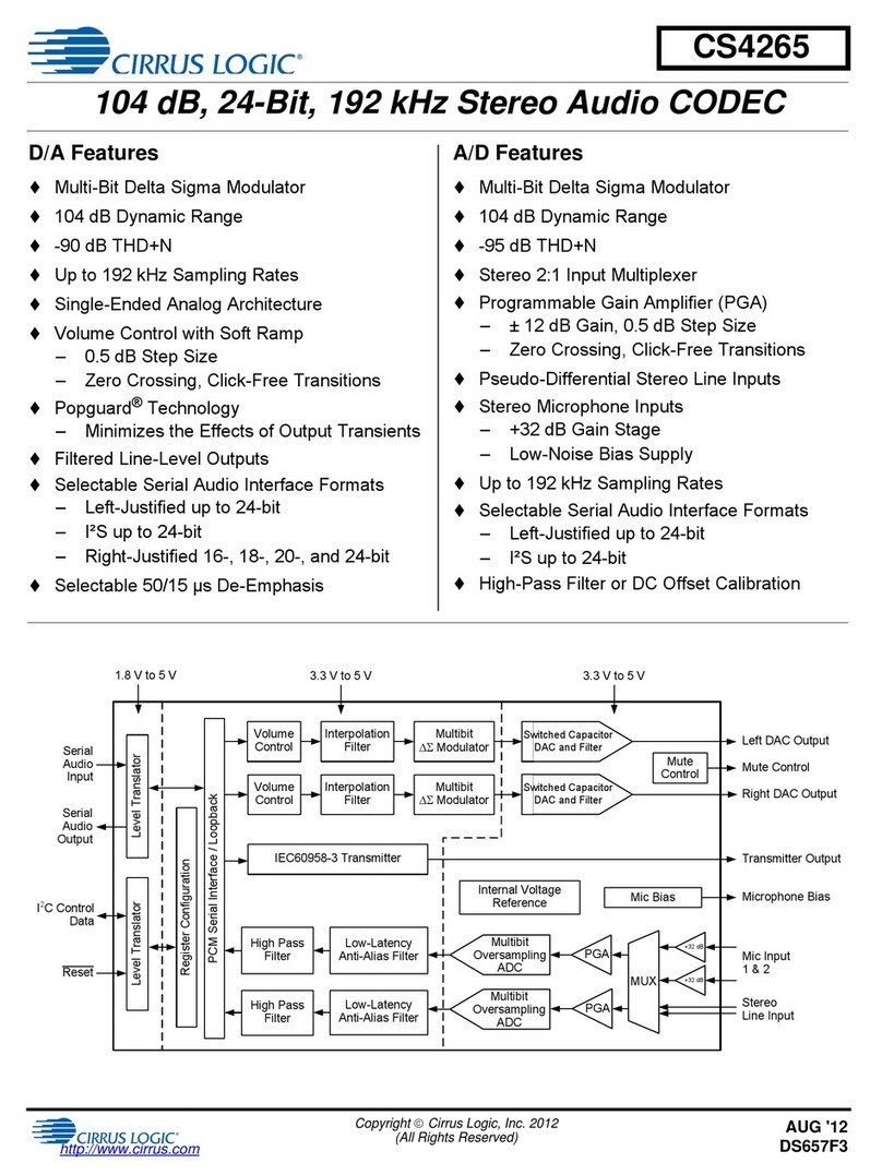
Stereo headphone (HP) output with 114-dB dynamic range
— Class H HP amplifier with four-level automatic or
manual supply adjust
— Power output 2 x 35 mW into 30
• Mono mic input with 114-dB dynamic range
— Low-noise headset bias with integrated bias resistor
—1-V
RMS input voltage
— Integrated AC-coupling capacitors
• Integrated detect features
— OMTP (Open Mobile Terminal Platform) and AHJ
(American headset jack) headset-type detection and
configuration with low-impedance internal switches
— Mic short (S0 Button) detect with ADC automute
— Automatic Hi-Z of headset bias output to ground on
headset bias current rise or HP/headset unplug
• System wake from headset/headphone plug/unplug or
S0 button press
• Interrupt output
• Mono equalizer for side-tone mix
•MIPI
® SoundWire™ or I2C/I2S/TDM control and audio
interface
• S/PDIF transmit (Sony/Philips digital interface format)
• Integrated fractional-N PLL
— Increases system-clock flexibility for audio processing
— Reference clock sourced from either I2S/TDM bit clock
or MIPI SoundWire clock
• Audio serial port (ASP)
—I
2S (two channels) or TDM (up to four channels)
— Slave or Hybrid-Master Mode (bit-clock slave and
LRCK/FSYNC derived from bit clock)
— Sample-rate converter (SRC) for two input channels,
with bypass
— SRC for one output channel, with bypass
— User isochronous audio transport support
— Supports up to 192-kHz sample rate to S/PDIF output
— Sample rate support for 8 to 192 kHz
• Integrated power management
— Digital core operates from either an external 1.2-V
supply or LDO from a 1.8-V supply.
— Step-down charge pump improves HP efficiency
— Independent peripheral power-down controls
— Standby operation from VP with all other supplies
powered off
— VP monitor to detect and report brownout conditions
— Low-impedance switching suppresses ground-noise
Applications
• Ultrabooks, tablets, and smartphones
• Digital headsets
CS42L42
PLL
Clock
Gen
MCLK
HPOUTB
–
VCP_ FILT
MCLK
HPOUTA
+VC P _F I LT
Interpolator
HSIN+
HSIN–
ADC
SWIRE_SD/
ASP_SDIN
SWIRE_CLK/
ASP_SCLK
DAC
DAC
ASP_SDOUT ASP_LRCK/
FSYNC
Decimators
Pseudodifferential Input
Headphone Detect
HS4
HS3
HS_CLAMP1
HS_CLAMP2
TIP_SENSE
INT
DAO
SoundWire
Audio and
Control
Port
DAI
SRC SRC SRC
2
HPF /
Mute
Windnoise
Filter EQ
22
2
Headset
Detect,
Switches,
and Depletion
FET Control
Interpolator
Downlink
WAKE
–
VCP_ FILT
+VCP_FILT
HS4_REF
HS3_REF
RING_SENSE
HS Bias LDO
VL VD_FILT
DIGLDO_PDN
+VCP_FILT
–VCP_FILT
VA
Inverting
Step-Down
LDO
VP
Analog
Core
POR
VCP
VP _CP
ADC
Mute
Mute
SWIRE_SEL
HPSENSA
Digital
Core
Downlink
–
+
–
+
HPSENSB
–
+
MCLK
SCLSDA
S/PDIF
I
2
C Slave
SPDIF_TXAD0 AD1
LDO
with
Bypass
CS42L42

DS1083F2 2
CS42L42
General Description
The CS42L42 is a low-power audio codec with integrated MIPI SoundWire interface or I2C/I2S/TDM interfaces designed
for portable applications. It provides a high-dynamic range, stereo DAC for audio playback and a mono
high-dynamic-range ADC for audio capture.
The CS42L42 provides high performance (up to 24-bit) audio for ADC and DAC audio playback and capture functions as
well as for the S/PDIF transmitter. The CS42L42 architecture includes bypassable SRCs and a bypassable, three-band,
32-bit parametric equalizer that allows processing of digital audio data.
A digital mixer is used to mix the ADC or serial ports to the DACs. There is independent attenuation on each mixer input.
The processing along the output paths from the ADC or serial port to the two stereo DACs includes volume adjustment
and mute control.
The CS42L42 is available in a 49-ball WLCSP package and a 48-pin QFN package for extended temperature range grade
of –40°C to +85°C.
Table of Contents
1 Pin Assignments and Descriptions . . . . . . . . . . . . . . . . . . . . . . 3
1.1 WLCSP Pin Out (Through-Package View) . . . . . . . . . . . . . . 3
1.2 QFN Pin Out (Through-Package View) . . . . . . . . . . . . . . . . . 4
1.3 Pin Descriptions . . . . . . . . . . . . . . . . . . . . . . . . . . . . . . . . . . 5
1.4 Electrostatic Discharge (ESD) Protection Circuitry . . . . . . . . 7
2 Typical Connections . . . . . . . . . . . . . . . . . . . . . . . . . . . . . . . . . . 9
2.1 Electromagnetic Compatibility (EMC) Circuitry . . . . . . . . . . 11
3 Characteristics and Specifications . . . . . . . . . . . . . . . . . . . . . 12
4 Functional Description . . . . . . . . . . . . . . . . . . . . . . . . . . . . . . . 29
4.1 Analog Input . . . . . . . . . . . . . . . . . . . . . . . . . . . . . . . . . . . . 31
4.2 Digital Mixer . . . . . . . . . . . . . . . . . . . . . . . . . . . . . . . . . . . . . 32
4.3 Three-Band Equalizer . . . . . . . . . . . . . . . . . . . . . . . . . . . . . 33
4.4 Analog Output . . . . . . . . . . . . . . . . . . . . . . . . . . . . . . . . . . . 36
4.5 System Headphone Parasitic Resistances . . . . . . . . . . . . . 39
4.6 Class H Amplifier . . . . . . . . . . . . . . . . . . . . . . . . . . . . . . . . . 41
4.7 Clocking Architecture . . . . . . . . . . . . . . . . . . . . . . . . . . . . . 46
4.8 SoundWire Interface . . . . . . . . . . . . . . . . . . . . . . . . . . . . . . 52
4.9 Audio Serial Port (ASP) . . . . . . . . . . . . . . . . . . . . . . . . . . . . 67
4.10 S/PDIF Tx Port . . . . . . . . . . . . . . . . . . . . . . . . . . . . . . . . . 73
4.11 Sample-Rate Converters (SRCs) . . . . . . . . . . . . . . . . . . . 75
4.12 Headset Interface . . . . . . . . . . . . . . . . . . . . . . . . . . . . . . . 76
4.13 Headset Type Detect . . . . . . . . . . . . . . . . . . . . . . . . . . . . . 78
4.14 Plug Presence Detect . . . . . . . . . . . . . . . . . . . . . . . . . . . . 79
4.15 Power-Supply Considerations . . . . . . . . . . . . . . . . . . . . . . 82
4.16 Control-Port Operation . . . . . . . . . . . . . . . . . . . . . . . . . . . 84
4.17 Reset . . . . . . . . . . . . . . . . . . . . . . . . . . . . . . . . . . . . . . . . . 86
4.18 Interrupts . . . . . . . . . . . . . . . . . . . . . . . . . . . . . . . . . . . . . . 87
5 System Applications . . . . . . . . . . . . . . . . . . . . . . . . . . . . . . . . . 89
5.1 Power-Up Sequence . . . . . . . . . . . . . . . . . . . . . . . . . . . . . 89
5.2 Power-Down Sequence . . . . . . . . . . . . . . . . . . . . . . . . . . . . 92
5.3 SoundWire Power Sequences . . . . . . . . . . . . . . . . . . . . . . 93
5.4 Page 0x30 Read Sequence . . . . . . . . . . . . . . . . . . . . . . . . 97
5.5 PLL Clocking . . . . . . . . . . . . . . . . . . . . . . . . . . . . . . . . . . . . 97
5.6 Standby Mode and Headset Clamps . . . . . . . . . . . . . . . . . . 97
5.7 Detection Sequence from Wake . . . . . . . . . . . . . . . . . . . . . 97
5.8 VD_FILT/VL ESD Diode . . . . . . . . . . . . . . . . . . . . . . . . . . 101
5.9 External Output Switch Considerations . . . . . . . . . . . . . . . 101
6 Register Quick Reference . . . . . . . . . . . . . . . . . . . . . . . . . . . 102
6.1 SoundWire Address Maps . . . . . . . . . . . . . . . . . . . . . . . . . 103
6.2 Slave Control Port Registers . . . . . . . . . . . . . . . . . . . . . . . 104
6.3 Slave Data Port 1–3, 15 Registers . . . . . . . . . . . . . . . . . . 105
6.4 Global Registers . . . . . . . . . . . . . . . . . . . . . . . . . . . . . . . . 106
6.5 Power-Down and Headset-Detect Registers . . . . . . . . . . . 107
6.6 Clocking Registers . . . . . . . . . . . . . . . . . . . . . . . . . . . . . . 108
6.7 Interrupt Registers . . . . . . . . . . . . . . . . . . . . . . . . . . . . . . . 108
6.8 Fractional-N PLL Registers . . . . . . . . . . . . . . . . . . . . . . . . 110
6.9 HP Load Detect Registers . . . . . . . . . . . . . . . . . . . . . . . . . 110
6.10 Headset Interface Registers . . . . . . . . . . . . . . . . . . . . . . 110
6.11 Headset Bias Registers . . . . . . . . . . . . . . . . . . . . . . . . . . 111
6.12 ADC Registers . . . . . . . . . . . . . . . . . . . . . . . . . . . . . . . . . 111
6.13 DAC Registers . . . . . . . . . . . . . . . . . . . . . . . . . . . . . . . . . 112
6.14 HP Control Registers . . . . . . . . . . . . . . . . . . . . . . . . . . . . 112
6.15 Class H Registers . . . . . . . . . . . . . . . . . . . . . . . . . . . . . . . 112
6.16 Mixer Volume Registers . . . . . . . . . . . . . . . . . . . . . . . . . . 112
6.17 Equalizer Registers . . . . . . . . . . . . . . . . . . . . . . . . . . . . . 113
6.18 AudioPort Interface Registers . . . . . . . . . . . . . . . . . . . . . 113
6.19 SRC Registers . . . . . . . . . . . . . . . . . . . . . . . . . . . . . . . . . 114
6.20 DMA Registers . . . . . . . . . . . . . . . . . . . . . . . . . . . . . . . . . 114
6.21 S/PDIF Registers . . . . . . . . . . . . . . . . . . . . . . . . . . . . . . . 114
6.22 Serial Port Transmit Registers . . . . . . . . . . . . . . . . . . . . . 115
6.23 Serial Port Receive Registers . . . . . . . . . . . . . . . . . . . . . 115
6.24 ID Registers . . . . . . . . . . . . . . . . . . . . . . . . . . . . . . . . . . . 116
7 Register Descriptions . . . . . . . . . . . . . . . . . . . . . . . . . . . . . . . 116
7.1 SoundWire Control Port 0 Registers . . . . . . . . . . . . . . . . . 117
7.2 SoundWire Data Port (1–3) Descriptions . . . . . . . . . . . . . . 123
7.3 Global Registers . . . . . . . . . . . . . . . . . . . . . . . . . . . . . . . . . 127
7.4 Power Down and Headset Detects . . . . . . . . . . . . . . . . . . 130
7.5 Clocking Registers . . . . . . . . . . . . . . . . . . . . . . . . . . . . . . . 136
7.6 Interrupt Registers . . . . . . . . . . . . . . . . . . . . . . . . . . . . . . . 139
7.7 Fractional-N PLL Registers . . . . . . . . . . . . . . . . . . . . . . . . 146
7.8 HP Load-Detect Registers . . . . . . . . . . . . . . . . . . . . . . . . . 148
7.9 Headset Interface Registers . . . . . . . . . . . . . . . . . . . . . . . . 148
7.10 Headset Bias Registers . . . . . . . . . . . . . . . . . . . . . . . . . . 152
7.11 ADC Registers . . . . . . . . . . . . . . . . . . . . . . . . . . . . . . . . . 153
7.12 DAC Control Registers . . . . . . . . . . . . . . . . . . . . . . . . . . . 154
7.13 HP Control Register . . . . . . . . . . . . . . . . . . . . . . . . . . . . . 155
7.14 Class H Register . . . . . . . . . . . . . . . . . . . . . . . . . . . . . . . 155
7.15 Mixer . . . . . . . . . . . . . . . . . . . . . . . . . . . . . . . . . . . . . . . . . 155
7.16 Equalizer . . . . . . . . . . . . . . . . . . . . . . . . . . . . . . . . . . . . . 156
7.17 AudioPort Interface Registers . . . . . . . . . . . . . . . . . . . . . 158
7.18 SRC Registers . . . . . . . . . . . . . . . . . . . . . . . . . . . . . . . . . 160
7.19 DMA Registers . . . . . . . . . . . . . . . . . . . . . . . . . . . . . . . . . 160
7.20 S/PDIF . . . . . . . . . . . . . . . . . . . . . . . . . . . . . . . . . . . . . . . 161
7.21 Serial Port Register Transmit Registers . . . . . . . . . . . . . . 162
7.22 Serial Port Receive Registers . . . . . . . . . . . . . . . . . . . . . 164
7.23 ID Registers . . . . . . . . . . . . . . . . . . . . . . . . . . . . . . . . . . . 168
8 PCB Layout Considerations . . . . . . . . . . . . . . . . . . . . . . . . . . 169
8.1 Power Supply . . . . . . . . . . . . . . . . . . . . . . . . . . . . . . . . . . . 169
8.2 Grounding . . . . . . . . . . . . . . . . . . . . . . . . . . . . . . . . . . . . . . 169
8.3 QFN Thermal Pad . . . . . . . . . . . . . . . . . . . . . . . . . . . . . . . 169
9 Plots . . . . . . . . . . . . . . . . . . . . . . . . . . . . . . . . . . . . . . . . . . . . . 170
9.1 Digital Filter Response . . . . . . . . . . . . . . . . . . . . . . . . . . . . 170
9.2 Windnoise Filter Responses . . . . . . . . . . . . . . . . . . . . . . . . 176
9.3 HSBIAS Current Sense vs. VP Voltage per Trip Setting . . 178
10 Package Dimensions . . . . . . . . . . . . . . . . . . . . . . . . . . . . . . . 179
10.1 WLCSP Package Dimensions . . . . . . . . . . . . . . . . . . . . . 179
10.2 QFN Package Dimensions . . . . . . . . . . . . . . . . . . . . . . . . 180
11 Thermal Characteristics . . . . . . . . . . . . . . . . . . . . . . . . . . . . 181
12 Ordering Information . . . . . . . . . . . . . . . . . . . . . . . . . . . . . . . 181
13 References . . . . . . . . . . . . . . . . . . . . . . . . . . . . . . . . . . . . . . . 181
14 Revision History . . . . . . . . . . . . . . . . . . . . . . . . . . . . . . . . . . . 182

DS1083F2 3
CS42L42
1 Pin Assignments and Descriptions
1 Pin Assignments and Descriptions
This section shows pin assignments and describes pin functions.
1.1 WLCSP Pin Out (Through-Package View)
Figure 1-1. WLCSP Pin Diagram (Through-Package View)
SDA SCL VL ASP_SDOUT ASP_SDIN/
SWIRE_SD
SPDIF_TX VD_FILT
VA AD1 GNDL ASP_SCLK/
SWIRE_CLK
ASP_LRCK/
FSYNC
GNDD INT
FILT+ GNDA AD0 VL_SEL RESET WAKE TSTI
HSIN– TSTI SWIRE_SEL DIGLDO_PDN HPSENSA VCP VP
HSIN+ HS_CLAMP2 HSBIAS_FILT_
REF
TIP_SENSE HPOUTA +VCP_FILT FLYP
HS4 HS_CLAMP1 HSBIAS_
FILT HS4_REF HPSENSB GNDCP FLYC
GNDHS HS3 RING_SENSE HS3_REF HPOUTB –VCP_FILT FLYN
A1
A2
A3
A4
A5
A6
A7
B1
B2
B3
B4
B5
B6
B7
C1
C2
C3
C4
C5
C6
C7
D1
D2
D3
D4
D5
D6
D7
E1
E2
E3
E4
E5
E6
E7
F1
F2
F3
F4
F5
F6
F7
G1
G2
G3
G4
G5
G6
G7
HeadphoneMicrophone Power
Charge
Pump Ground
Digital I/O

DS1083F2 4
CS42L42
1.2 QFN Pin Out (Through-Package View)
1.2 QFN Pin Out (Through-Package View)
Figure 1-2. QFN Pin Diagram
Top- D ow n (Through Package ) View
48 -Pin QFN Package
12
7
6
5
4
3
2
1
11
10
9
8
25
30
31
32
33
34
35
36
26
27
28
29
1413 15 16 17 18 19 20 21 22 23 24
4748 46 45 44 43 42 41 40 39 38 37
SDA
AD0
AD1
VA
FILT+
GNDA
HSIN–
HSIN+
HS4
HS_CLAMP2
HS_CLAMP1
GNDHS
RESET
INT
WAKE
DIGLDO_PDN
TSTI1
VP
VCP
FLYP
FLYC
+VCP_FILT
FLYN
GNDCP
VL_SEL
VD_FILT
GNDD
SPDIF_TX
ASP_SDIN/SWIRE_SD
ASP_LRCK/FSYNC
ASP_SCLK/SWIRE_CLK
ASP_SDOUT
SWIRE_SEL
VL
GNDL
SCL
–VCP_FILT
HPSENSA
HPOUTA
HPOUTB
HPSENSB
TIP_SENSE
HS3_REF
HS4_REF
RING_SENSE
HSBIAS_FILT
HSBIAS_FILT_REF
HS3
–VCP_FILT
HPSENSA
HPOUTA
HPOUTB
HPSENSB
TIP_SENSE
HS3_REF
HS4_REF
RING_SENSE
HSBIAS_FILT
HS3

DS1083F2 5
CS42L42
1.3 Pin Descriptions
1.3 Pin Descriptions
Table 1-1. Pin Descriptions
Pin Name CSP
Pin #
QFN
Pin #
Power
Supply I/O Pin Description
Internal
Connection
Driver Receiver State at
Reset
HS_CLAMP1
HS_CLAMP2
F2
E2
26
27
VP I
Headset Depletion FET Connections.
Input to drain of
integrated depletion FET for ground-noise rejection.
— — — Input
HS3_REF
HS4_REF
G4
F4 19
20 VP I Headset Connection Reference. Input to
pseudodifferential HP output reference
— — — Input
HS3
HS4
G2
F1 24
28 VP I Headset Connections. Input to headset and
mic-button detection functions
— — — Input
HSBIAS_FILT F3 22 VP I Headset Bias Source Voltage Filter. Filter
connection for the internal quiescent voltage used for
headset bias generation.
— — — Input
HSBIAS_FILT_
REF
E3 23 VP I Headset Bias Source Voltage Filter Reference.
Input of filter connection for the internal quiescent
voltage used for headset-bias generation.
— — — Input
HSIN– D1 30 VP I
Inverting Mic Inputs.
Inverting analog input for the ADC.
— — — Input
HSIN+ E1 29 VP I Noninverting Mic Inputs. Noninverting analog input
for the ADC.
— — — Input
RING_SENSE G3 21 VP I Ring Sense Input. Sense pin to detect S/PDIF or
headphone plug. Can be configured to be debounced
on plug and unplug events independently.
— — — Input
HPOUTA
HPOUTB
E5
G5
15
16 ±VCP_
FILT
OHeadphone Audio Output. Ground-centered audio
output.
————
HPSENSA
HPSENSB
D5
F5 14
17
±VCP_
FILT
IHeadphone Audio Sense Input. Audio sense input. — — — Input
TIP_SENSE E4 18 VP I Tip Sense. Output can be set to wake the system.
Independently configurable to be debounced on plug
and unplug events.
—Hi-Z——
AD0
AD1
C3
B2
35
34 VL I I2C Address Input/SoundWire Instance ID Input.
Address pins for I2C or SoundWire Instance ID [1:0]
input.
— — Hysteresis
on CMOS
input
Input
ASP_LRCK/
FSYNC
B5 43 VL I/O ASP Left/Right Clock or Frame Sync. Left or right
word select, or frame start sync for the ASP interface.
—CMOS
output
Hysteresis
on CMOS
input
Input
ASP_SCLK/
SWIRE_CLK
B4 42 VL I ASP/SoundWire Serial Data Clock. SoundWire
data-shift clock in SoundWire Mode or serial
data-shift clock for the ASP interface in I2S/TDM
Mode. Source clock used for internal master clock
generation.
— — Hysteresis
on CMOS
input
Input
ASP_SDIN/
SWIRE_SD
A5 44 VL I/O ASP Serial Data Input/SoundWire Serial Data
Input and Output. Serial data input and output in
SoundWire mode or serial data input for the ASP
interface in I2S/TDM mode.
—CMOS
output
Hysteresis
on CMOS
input
Input
ASP_SDOUT A4 41 VL O ASP Serial Data Output. Serial data output for the
ASP interface.
Weak
pull-down
CMOS
output
— Output
DIGLDO_PDN D4 4VP I Digital LDO Power Down. Digital core logic LDO
power down.
— — Hysteresis
on CMOS
input
Input
INT B7 2 VP O Interrupt output. Programmable, open-drain,
active-low programmable interrupt output.
—CMOS
open-drain
output
— Output
RESET C5 1 VP I Reset. Hardware reset. — — Hysteresis
on CMOS
input
Input
SCL A2 37 VL I I2C Clock. Clock input for the I2C interface. — — Hysteresis
on CMOS
input
Input
Microphone
Headphone
Digital I/O

DS1083F2 6
CS42L42
1.3 Pin Descriptions
SDA A1 36 VL I/O I2C Input/Output. I2C input and output. — CMOS
open-drain
output
Hysteresis
on CMOS
input
Input
SPDIF_TX A6 45 VL O S/PDIF Audio Serial Data Output. Serial data
output for S/PDIF interface.
—CMOS
output
— Output
SWIRE_SEL D3 40 VL I SoundWire Select. SoundWire interface selection
input. Defines the serial and audio interface type. If
asserted, SoundWire is the control and audio
interface, otherwise I2C is control and TDM/I2S is
used for audio data.
— — Hysteresis
on CMOS
input
Input
VL_SEL C4 48 VP I VL Supply Voltage Select. Select for VL power
supply voltage level. Connect to VP for 1.8-V VL
supply, connect to GNDD for 1.2-V VL supply
— — Hysteresis
on CMOS
input
Input
WAKE C6 3 VP O Wake up. Programmable, open-drain, active-low
output. This outputs the state of the Mic S0 or HP
wake detect.
—Hi-Z,
CMOS
open-drain
output
— Output
–VCP_FILT G6 13 VCP/
VP1
OInverting Charge Pump Filter Connection. Power
supply for the inverting charge pump that provides
the negative rail for the HP amplifier.
————
+VCP_FILT E6 10 VCP/
VP1
OStep Down Charge Pump Filter Connection.
Power supply for the step down charge pump that
provides the positive rail for the HP amplifier.
————
FLYC F7 9VCP/
VP1
OCharge Pump Cap Common Node. Common
positive node for the HP amplifiers’ step-down and
inverting charge pumps’ flying capacitors.
————
FLYN G7 11 VCP/
VP1
OCharge Pump Cap Negative Node. Negative node
for the inverting charge pump’s flying capacitor.
————
FLYP E7 8VCP/
VP1
OCharge Pump Cap Positive Node. Positive node for
HP amps’ step-down charge pump’s flying capacitor.
————
FILT+ C1 32 VA I Positive Voltage Reference. Positive reference
voltage for internal sampling circuits.
————
VA B1 33 N/A I Analog Power Supply. Power supply for the internal
analog section.
————
VCP D6 7N/A I Charge Pump Power. Power supply for the internal
HP amplifiers charge pump.
————
VD_FILT A7 47 N/A I 1.2-V Digital Core Power Supply. Power supply for
internal digital logic.
————
VL A3 39 N/A I I/O Power Supply. Power supply for external
interface and internal digital logic.
————
VP D7 6N/A I High Voltage Interface Supply. Power supply for
high voltage interface.
————
GNDA C2 31 N/A I Analog Ground. Ground reference for the internal
analog section.
————
GNDL B3 38 N/A I Digital Ground. Ground reference for interface
section.
————
GNDHS G1 25 N/A I Headset Ground. Ground reference for the internal
analog section.
————
GNDCP F6 12 N/A I Charge Pump Ground. Ground reference for the
internal HP amplifiers charge pump.
————
GNDD B6 46 N/A I Digital Ground. Ground reference for the internal
digital circuits.
————
TSTI D2, C7 —N/AITest input. Connect to GNDA. — — — —
1.The power supply is determined by ADPTPWR setting (see Section 7.14.1). VP is used if ADPTPWR = 001 (VP_CP Mode) or when necessary for
ADPTPWR = 111 (Adapt-to-Signal Mode).
Table 1-1. Pin Descriptions (Cont.)
Pin Name CSP
Pin #
QFN
Pin #
Power
Supply I/O Pin Description
Internal
Connection
Driver Receiver State at
Reset
Charge Pump
Power
Ground
Test

DS1083F2 7
CS42L42
1.4 Electrostatic Discharge (ESD) Protection Circuitry
1.4 Electrostatic Discharge (ESD) Protection Circuitry
Fig. 1-3 provides a composite view of the ESD domains showing the ESD protection paths between each pad and the
substrate (GNDA) and the interrelations between some domains. Note that this figure represents the structure for the
internal protection devices and that additional protections can be implemented as part of the integration into the board.
Figure 1-3. Composite ESD Topology
Table 1-2 shows the individual ESD domains and lists the pins associated with each domain.
ESD-sensitive device. The CS42L42 is manufactured on a CMOS process. Therefore, it is generically
susceptible to damage from excessive static voltages. Proper ESD precautions must be taken while
handling and storing this device. This device is qualified to current JEDEC ESD standards.
Table 1-2. ESD Domains
ESD
Domain
Signal Name (CSP/QFN)
(See * in Topology Figures for Pad) Topology
VL/
GNDA 1
AD0
AD1
ASP_LRCK/FSYNC
GNDL
SCL
SDA
ASP_SDOUT
SPDIF_TX
SWIRE_SEL
ASP_SCLK/SWIRE_CLK
SWIRE_SD/ASP_SDIN
VD_FILT
VL
VD_FILT/
GNDA
VD_FILT
GNDD
TSTI
VA/
GNDA
FILT+
GNDA
VA
GNDL
VL
Substrate
(GNDA)
VA VCP
GNDA
Substrate
(GNDA)
GNDCP
+VCP_FILTVP
–VCP_FILT
GNDHS
____________________
VL/GNDA Domain
____________________
VA/GNDA Domain
__________
VCP/GNDA
Domain
VP/GNDA Domain
_______________
VD_FILT/GNDA
Domain
VP/–VCP_FILT Domain
–VCP_FILT/+VCP_FILT Domain
GNDD
VD_FILT
Note: The asterisks indicate the pads with which the individual
pins from the corresponding domains are associated. These
pins are listed in Table 1-2.
***
*
*
GNDL
VL
Substrate
(GNDA)
VD_FILT
*
Substrate
(GNDA)
GNDD
VD_FILTVL
*
Substrate
(GNDA)
GNDA
VA
*

DS1083F2 8
CS42L42
1.4 Electrostatic Discharge (ESD) Protection Circuitry
VCP/
GNDA
VCP
VP/
GNDA
GNDHS
HS3
HS4
HS_CLAMP1
HS_CLAMP2
HSBIAS_FILT
HSBIAS_FILT_REF
HSIN+
HSIN–
VP
VL_SEL
INT
WAKE
RESET
DIGLDO_PDN
+VCP_
FILT/
–VCP_
FILT
+VCP_FILT
–VCP_FILT
FLYN
HPSENSA
HPSENSB
HPOUTA
HPOUTB
GNDCP
VP/
–VCP_
FILT
FLYC
FLYP
HS3_REF
HS4_REF
RING_SENSE
TIP_SENSE
1.See Section 5.8 for additional information regarding VD_FILT andVL.
Table 1-2. ESD Domains (Cont.)
ESD
Domain
Signal Name (CSP/QFN)
(See * in Topology Figures for Pad) Topology
VCP
Substrate
(GNDA)
Substrate
(GNDA)
GNDCP
+VCP_FILTVP
–VCP_FILT
Substrate
(GNDA)
GNDHS
VP/GNDA Domain
VP/–VCP_FILT Domain
+VCP_FILT/–VCP_FILT Domain
**
*

DS1083F2 9
CS42L42
2 Typical Connections
2 Typical Connections
Figure 2-1. Typical Connection Diagram for I2C, I2S, or TDM
R
P_I
R
P_ I2 C
R
P_W
Applications
Processor
PMU
VA
2.2 µF
*
Battery
(3.0–5.0 V)
FLYC
FLYN
2.2 µF
FLYP
2.2 µF
*
*
+VCP_FILT
–VCP_FILT
2.2 µF2.2 µF
GNDCP
**
All external passive component
values shown are nominal.
Key for Capacitor Types Required:
* Use low ESR, X7R/X5R capacitors
If no type symbol is shown next to a
capacitor, any type may be used.
FILT+
10 µF
*
VP
4.7 µF
*
HSBIAS_FILT_REF
HSBIAS_FILT
4.7 µF
*
ASP_LRCK/FSYNC
ASP_SCLK/SWIRE_CLK
SWIRE_SD/ASP_SDIN
ASP_SDOUT
1.8 V
GNDA
SDA
SCL
WAKE
INT
VL
1.8 V/1.2 V
RESET
VCP
VD_FILT
See
DIGLDO_PDN
and VL_SEL
Configurations
DIGLDO_PDN
AD0
GNDL
AD1
2.2 µF
*
VL_SEL
GNDD
HSIN+
HSIN–
HPOUTB
TIP_SENSE
HPOUTA
HS3
Headset Connector
HS4
Headphone
Output Filter
HS3_REF
HS4_REF
SPDIF_TX
RING_SENSE
GNDHS
HS_CLAMP1
HS_CLAMP2
DIGLDO_PDN and VL_SEL
Configurations
DIGLDO_PDN = 1 (3.0 to 5.0 V)
VL
VD_FILT
DIGLDO_PDN
0.1 µF
*
1.8 V
DIGLDO_PDN = 0 (GNDD)
VL
VD_FILT
1 µF
*
1.2 V DIGLDO_PDN
0.1 µF
*
Opt ical
Transmitter
Module
DIGLDO_PDN = 0 (GNDD)
VL
VD_FILT
1 µF
*
1.8 V DIGLDO_PDN
0.1 µF
*
1.2 V
HPSENSB
HPSENSA
SWIRE_SEL
VL_SEL
VL_SEL = 0 (GNDD)
VL_SEL
Battery
(VP = 3.0 to 5.0V)
VL_SEL = 1 (3.0 to 5.0 V)
VL_SEL = 1 (3.0 to 5.0 V)
VL_SEL
Battery
(VP = 3.0 to 5.0V)
VL or VP
VL or VP
Note 3
Note 4
Note 5
Note 6
CS42L42
Note 1
Note 1
TSTI

DS1083F2 10
CS42L42
2 Typical Connections
Figure 2-2. Typical Connection Diagram for SoundWire
Notes:
1. RP_I and RP_W values can be determined by the INT and WAKE pin specifications in Tabl e 3- 2 5.
2. HPSENSA and HPSENSB are supported only on the WLCSP package.
3. RP_I2C values can be determined by the I2C pull-up resistance specification in Table 3-24.
4. The headphone amplifier’s output power and distortion ratings use the nominal capacitances shown. Larger capacitance reduces ripple on
the internal amplifiers’ supplies and, in turn, reduces distortion at high-output power levels. Smaller capacitance may not reduce ripple
enough to achieve output power and distortion ratings. Because actual values of typical X7R/X5R ceramic capacitors deviate from nominal
values by a percentage specified in the manufacturer’s data sheet, capacitors must be selected for minimum output power and maximum
distortion required. Higher value capacitors than those shown may be used, however lower value capacitors must not (values can vary from
the nominal by ±20%). See Section 2.1.2 for additional details.
5. Series resistance in the path of the power supplies must be avoided. Any voltage drop on VCP directly affects the negative charge-pump
supply (–VCP_FILT) and clips the audio output.
6. Lowering capacitance below the value shown affects PSRR, THD+N performance, ADC–DAC isolation and intermodulation, and
interchannel isolation and intermodulation.
HSIN+
HSIN–
HPOUTB
TIP_SENSE
HPOUTA
HS3
Headset Connector
HS4
Headphone
Output Filt er
HS3_REF
HS4_REF
SPDIF_TX
RING_SENSE
Optical
Transmitter
Module
DIGLDO_PDN and VL_SEL
Configurations
DIGLDO_PDN = 1 (3.0 to 5.0 V)
VL
VD_FILT
DIGLDO_PDN
0.1 µF
*
1.8 V
DIGLDO_PDN = 0 (GNDD)
VL
VD_FILT
1 µF
*
1.2 V DIGLDO_PDN
0.1 µF
*
DIGLDO_PDN = 0 (GNDD)
VL
VD_FILT
1 µF
*
1.8 V DIGLDO_PDN
0.1 µF
*
1.2 V
VL_SEL
VL_SEL = 0 (GNDD)
VL_SEL
Battery
(VP = 3.0 to 5.0V)
VL_SEL = 1 (3.0 to 5.0 V)
VL_SEL = 1 (3.0 to 5.0 V)
VL_SEL
Battery
(VP = 3.0 to 5.0V)
GNDHS
FLYC
FLYN
2.2 µF
FLYP
2.2 µF
*
*
+VCP_FILT
–VCP_FILT
2.2 µF2.2 µF
GNDCP
**
FILT+
10 µF
*
VP
4.7 µF
*
HSBIAS_FILT_REF
HSBIAS_FILT
4.7 µF
*
GNDA
SDA
SCL
_____
WAKE
RESET
VCP
2.2 µF
*
All external passive component
values shown are nominal.
Key for Capacitor Types Required:
* Use low ESR, X7R/X5R capacitors
If no type symbol is shown next to a
capacitor, any type may be used.
VA
2.2 µF
VL
VD_FILT
See
DIGLDO_PDN
and VL_SEL
Configurations
DIGLDO_PDN
VL_SEL
ASP_LRCK/FSYNC
ASP_SCLK/SWIRE_CLK
SWIRE_SD/ASP_SDIN
ASP_SDOUT
AD0
GNDL
AD1
GNDD
SWIRE_SEL
R
P_W
PMU
Battery
(3.0–5.0 V) 1.8 V 1.8 V/1.2 V VL or VP
R
P_I
Applications
Processor
INT
VL or VP
Optional Connections
Note 1
Note 5
Note 4
Note 6
CS42L42
Note 1
TSTI

DS1083F2 11
CS42L42
2.1 Electromagnetic Compatibility (EMC) Circuitry
2.1 Electromagnetic Compatibility (EMC) Circuitry
The circuit in Fig. 2-3 may be applied to signals not local to the CS42L42 (i.e., that traverse significant distances) for EMC.
Figure 2-3. Optional EMC Circuit
2.1.1 Low-Profile Charge-Pump Capacitors
In the typical connection for analog mics (
Fig. 2-1
), the recommended capacitor values for the charge-pump circuitry are
2.2 µF, rated as X7R/X5R or better. The following low-profile versions of these capacitors are suitable for the application:
• Description: 2.2 µF ±20%, 6.3 V, X5R, 0201
• Manufacturer, Part Number: Murata, GRM033R60J225ME47, nominal height = 0.3 mm
• Manufacturer, Part Number: AVX, 02016D225MAT2A, nominal height = 0.33 mm
Note: Although the 0201 capacitors described are suitable, larger capacitors such as 0402 or larger may provide
acceptable performance.
2.1.2 Ceramic Capacitor Derating
Note 4 in
Fig. 2-1
highlights that ceramic capacitor derating factors can significantly affect in-circuit capacitance values
and, in turn, CS42L42 performance. Under typical conditions, numerous types and brands of large-value ceramic
capacitors in small packages exhibit effective capacitances well below their ±20% tolerance, with some being derated by
as much as –50%. These same capacitors, when tested by a multimeter, read much closer to their rated value. A similar
derating effect has not been observed with tantalum capacitors.
The derating observed varied with manufacturer and physical size: Larger capacitors performed better, as did ones from
Kemet Electronics Corp. and TDK Corp. of any size. This derating effect is described in data sheets and in applications
notes from capacitor manufacturers. For instance, as DC and AC voltages are varied from the standard test points (applied
DC and AC voltages for standard test points versus PSRR test are 0 and 1 VRMS @ 1 kHz versus 0.9 V and ~1 mVRMS
@ 20 Hz–20 kHz), it is documented that the capacitances vary significantly.
To/from
other
circuits
To/from DUT
27 pF
X7R
D1
L1 L2
L1 and L2: Ferrite:
f
Transition
= 30–100 MHz
DCR = 0.09–0.30
D1: Transorb:
V
Breakdown
> Normal operating peak
voltage of signal
Notes:

DS1083F2 12
CS42L42
3 Characteristics and Specifications
3 Characteristics and Specifications
Table 3-1 defines parameters as they are characterized in this section.
Table 3-1. Parameter Definitions
Parameter Definition
Dynamic range The ratio of the rms value of the signal to the rms sum of all other spectral components over the specified bandwidth. A
signal-to-noise ratio measurement over the specified bandwidth made with a –60 dB signal; 60 dB is added to resulting
measurement to refer the measurement to full scale. This technique ensures that distortion components are below the noise
level and do not affect the measurement. This measurement technique has been accepted by the Audio Engineering Society,
AES17–1991, and the Electronic Industries Association of Japan, EIAJ CP–307. Dynamic range is expressed in decibel units.
Idle channel
noise
The rms value of the signal with no input applied (properly back-terminated analog input, digital zero, or zero modulation input).
Measured over the specified bandwidth.
Interchannel
isolation
A measure of cross talk between the left and right channel pairs. Interchannel isolation is measured for each channel at the
converter's output with no signal to the input under test and a full-scale signal applied to the other channel. Interchannel
isolation is expressed in decibel units.
Load
resistance and
capacitance
The recommended minimum resistance and maximum capacitance required for the internal op-amp's stability and signal
integrity. The load capacitance effectively moves the band-limiting pole of the amp in the output stage. Increasing load
capacitance beyond the recommended value can cause the internal op-amp to become unstable.
Offset error The deviation of the midscale transition (111…111 to 000…000) from the ideal.
Output offset
voltage
The DC offset voltage present at the amplifier’s output when its input signal is in a mute state. The offset exists due to CMOS
process limitations and is proportional to analog volume settings. When measuring the offset out the headphone amplifier, the
headphone amplifier is ON.
Total harmonic
distortion +
noise (THD+N)
The ratio of the rms sum of distortion and noise spectral components across the specified bandwidth (typically 20 Hz–20 kHz)
relative to the rms value of the signal. THD+N is measured at –1 and –20 dBFS for the analog input and at 0 and –20 dB for
the analog output, as suggested in AES17–1991 Annex A. THD+N is expressed in decibel units.
Table 3-2. Recommended Operating Conditions
Test conditions: GNDA = GNDL = GNDCP = 0 V; voltages are with respect to ground.
Parameters Symbol Minimum 1
1.Device functional operation is guaranteed within these limits; operation outside them is not guaranteed or implied and may reduce device reliability.
Maximum 1Unit
DC power
supply
Charge pump VCP 1.66 1.94 V
LDO regulator for digital 2
2.If DIGLDO_PDN is deasserted, no external voltage must be applied to VD_FILT.
DIGLDO_PDN = 0 and VL_SEL = 0 VD_FILT 1.10 1.30 V
Serial interface control port
and S/PDIF transmitter DIGLDO_PDN = 0 and VL_SEL = 0
VL_SEL = 1
VL
VL
1.10
1.66
1.30
1.94
V
V
Analog VA 1.66 1.94 V
Battery supply VP 2.50 3
3.Although device operation is guaranteed down to 2.5 V, device performance is guaranteed only down to 3.0 V. The following are affected when
VP < 3.0 V: HSBIAS, charge pump LDO, TIP_SENSE threshold, RING_SENSE threshold.
5.25 V
External voltage
applied to pin 4,5
4.The maximum over/undervoltage is limited by the input current.
5.Table 1-1 lists the power supply domain in which each CS42L42 pin resides.
TIP_SENSE pin
±VCP_FILT domain pins 6
VL domain pins
VA domain pins
VP domain pins
6.±VCP_FILT is specified in Table 3-16.
VINHI
VVCPF
VVL
VVA
VVP
–VCP_FILT – 0.3
–VCP_FILT – 0.3
–0.3
–0.3
–0.3
VP + 0.3
+VCP_FILT + 0.3
VL + 0.3
VA + 0.3
VP + 0.3
V
V
V
V
V
Ambient temperature TA–40 +85 C
Table 3-3. Absolute Maximum Ratings
Test conditions: GNDA = GNDL = GNDCP = 0 V; voltages are with respect to ground.
Parameters Symbol Minimum Maximum Unit
DC power supply Charge pump, LDO, serial/control, analog (see Section 4.15)
Digital core
Battery
VL, VA, VCP
VD_FILT
VP
–0.3
–0.3
–0.3
2.33
1.55
6.3
V
V
V
Input current 1
1.Any pin except supply pins. Transient currents of up to ±100 mA on analog input pins do not cause SCR latch-up.
Iin —±10 mA
Ambient operating temperature (power applied) TA–50 +115 °C
Storage temperature Tstg –65 +150 °C
Caution: Stresses beyond “Absolute Maximum Ratings” levels may cause permanent damage to the device. These levels are stress ratings
only, and functional operation of the device at these or any other conditions beyond those indicated in Ta bl e 3- 2, “Recommended Operating
Conditions” is not implied. Exposure to absolute maximum rating conditions for extended periods may affect device reliability.

DS1083F2 13
CS42L42
3 Characteristics and Specifications
Table 3-4. Output Fault Rating
Test conditions: GNDA =GNDCP= 0 V; VA =1.8 V; VP =3.6 V; voltages are with respect to ground.
Source 1
1.Each source is individually connected directly to the specified supply during a fault condition.
Fault Supply Expected Years 2
2.The rating is based on foundry electromigration design rules when a perpetual fault exists on the HP outputs. When the specified time expires, analog
performance is expected to degrade.
HPOUT(A,B) VA
GNDA
+VCP_FILT
–VCP_FILT
VP
1.5
2
0.5
1.5
1.5
HS3/HS4 (HSx switch to ground) HPOUT(A,B)3
3.HPOUTx = 1 Vrms. If shorted to HSx, the headphone may be current limited in this configuration.
3.2
HS3/HS4 (HSx switches to HSBIAS) HPOUT(A,B)30.75
HS3_REF/HS4_REF (HSx connected to ground) HPOUT(A,B) 3.2
HS3_REF/HS4_REF (HSx not connected to ground) HPOUT(A,B) 0.75
Table 3-5. Combined High-Performance ADC On-Chip Analog and Digital Filter Characteristics
Test conditions (unless specified otherwise): TA = +25°C; MCLK = 12 MHz; MCLK_SRC_SEL = 0; FsINT = 48 kHz; path is HSIN to internal routing engine.
All gains are set to 0 dB; HPF disabled.
Parameter 1,2
1.Response scales with Fsint (internal sample rate, based on MCLK). Specifications are normalized to Fsint and are denormalized by multiplying by Fsint.
2.Measurements with HPF disabled require either differential configuration or single-ended configuration with –30 dBFS input signal.
Min Typical Max Unit
Notch filter on
(ADC_NOTCH_
DIS = 0)
Passband (normalized to 0.417x10⁻³ FsINT) –0.18-dB corner
–3.0-dB corner
—
—
0.390
0.410
—
—
Fsint
Fsint
Passband ripple (0.417x10⁻³ FsINT to 0.390 FsINT
; normalized to 0.417x10⁻³ Fsint)–0.23 — 0.15 dB
Stopband attenuation 1 (0.5 FsINT to 0.524 FsINT)45——dB
Stopband attenuation 2 (0.524 FsINT to 3 FsINT)70——dB
Total group delay 3
3.Informational only; group delay cannot be measured for this block by itself.Total group delay includes delay through the entire ADC and decimator
path total-group delay is measured at 1 kHz.
— 5.6/Fsint —s
Notch filter off
(ADC_NOTCH_
DIS = 1)
Passband (normalized to 0.417x10⁻³ FsINT) –0.05-dB corner
–3.0-dB corner
—
—
0.390
0.500
—
—
Fsint
Fsint
Passband ripple (0.417x10⁻³ FsINT to 0.417 FsINT
; normalized to 0.417x10⁻³ FsINT)–0.29 — 0.15 dB
Stopband attenuation (0.64 FsINT to 3 FsINT)70——dB
Total group delay 3— 5.6/Fsint —s
Table 3-6. ADC High-Pass Filter (HPF) Characteristics
Test conditions (unless specified otherwise): ADC_HPF_CF = 00; all gains are set to 0 dB; specifications represent the frequency response of the
entire path with ADC_NOTCH_DIS = 1, SRC_ADC_BYPASS = 1, ADC_WNF_EN = 0, and ADC_HPF_EN = 1.
Parameter 1
1.Response scales with Fs
INT
(based on internal MCLK). Specifications are normalized to Fs
INT
and are denormalized by multiplying by Fs
INT
.
Minimum Typical Maximum Unit
Passband (normalized to 0.2083 FSINT) –0.05-dB corner
–3.0-dB corner
—
—
0.666 x 10⁻³
77.0 x 10⁻⁶
—
—
FsINT
FsINT
Phase deviation @ 0.453 x 10⁻³ FsINT [2]
2.An additional –2° phase deviation may be present through the total path from HSIN to SDOUT.
— 12.37 — Deg
Filter settling time 3
3.Required time for the magnitude of the DC component present at the output of the HPF to reach 5% of the applied DC signal.
ADC_HPF_CF = 00 (38.8 x 10⁻⁶ x FsINT mode)
ADC_HPF_CF = 01 (2.5 x 10⁻³ x FsINT mode)
ADC_HPF_CF = 10 (4.9 x 10⁻³ x FsINT mode)
ADC_HPF_CF = 11 (9.7 x 10⁻³ x FsINT mode)
—
—
—
—
2900/FsINT
170/FsINT
90/FsINT
50/FsINT
—
—
—
—
s
s
s
s
Table 3-7. Combined DAC Digital, On-Chip Analog, and HPOUTx Filter Characteristics
Test conditions (unless specified otherwise): TA = +25°C; MCLK = 12 MHz, MCLK_SRC_SEL = 0, FsINT = 48 kHz; path is internal routing engine to
HPOUTx, analog and digital gains are all set to 0 dB; HPF disabled.
Parameter 1
1. Response scales with Fs
INT
(based on internal MCLK). Specifications are normalized to Fs
INT
and denormalized by multiplying by Fs
INT
.
Minimum Typical Maximum Unit
Passband –0.05-dB corner
–3.0-dB corner
—
—
0.48
0.50
—
—
FsINT
FsINT
Passband ripple (0.417x10⁻³ FsINT to 0.417 FsINT
; normalized to 0.417x10⁻³ FsINT) –0.04 — 0.063 dB
Stopband attenuation (0.545 FsINT to FsINT) 60 — — dB
Total group delay 2
2.Informational only; group delay cannot be measured for this block by itself.
An additional
5.5/Fsint
group delay
may be present through
the serial ports
and internal audio bus.
— 5.35/FsINT —s

DS1083F2 14
CS42L42
3 Characteristics and Specifications
Table 3-8. DAC High-Pass Filter (HPF) Characteristics
Test conditions (unless specified otherwise) Analog and digital gains are all set to 0 dB; TA = +25°C.
Parameter 1
1.Response scales with Fs
INT
(internal sample rate, based on MCLK). Specifications are normalized to Fs
INT
and are denormalized by multiplying by Fs
INT
.
Minimum Typical Maximum Unit
Passband –0.05-dB corner
–3.0-dB corner
—
—
0.180x10⁻³
19.5x10⁻⁶
—
—
FsINT
FsINT
Passband ripple (0.417x10⁻³ FsINT to 0.417 FsINT
; normalized to 0.417 FsINT)——0.01dB
Phase deviation @ 0.453x10⁻³ FsINT —2.45—°
Filter settling time 2
2.Required time for the magnitude of the DC component present at the output of the HPF to reach 5% of the applied DC signal.
— 24.5x10³/FsINT —s
Table 3-9. HSINx to SDOUT with SRC-Enabled Datapath Characteristics
Test conditions (unless specified otherwise): LRCK = FsINT = FsEXT = 48 kHz; MCLK = 12 MHz; HPF disabled; passband/stopband levels normalized
to 20 Hz; entire path characteristics including AFE + ADC + SRC + serial port.
Parameters 1,2
1.FsEXT is the external sample rate (LRCK/FSYNC frequency). Response scales with FsEXT.
2.Measurements with HPF disabled require either differential configuration or single-ended configuration with –30 dBFS input signal.
Minimum Typical Maximum Unit
ADC
notch
filter
enabled
Passband –0.22-dB corner
–3.0-dB corner
—
—
0.390
0.410
—
—
FsEXT
FsEXT
Passband ripple (0.417x10
–3
Fs
EXT
to 0.390 Fs
EXT
; normalized to 20 Hz)
–0.30 — 0.15 dB
Stopband rejection from 0.477 FsEXT to 3 FsEXT 70 — — dB
Square wave overshoot — — 3.1 dB
Group delay, bark-weighted average — — 38.5/FsEXT s
Group delay
Fs
EXT
44.1 kHz
Fs
EXT
48 kHz)
—
—
17.4/Fs
INT
+ (13.2 ± 1.5)/Fs
EXT
(12.4 ± 0.5)/Fs
INT
+ (11.9 ± 1)/Fs
EXT
—
—
s
s
SRC-disabled group delay 3
3.This value varies by up to 1 Fs. If SRC is disabled, Fs = FsOUT = FsIN.
—
(13.9
±
1)/Fs — s
ADC
notch
filter
disabled
Passband –0.22-dB corner
–3.0-dB corner
—
—
0.444
0.466
—
—
FsEXT
FsEXT
Passband ripple (0.417x10
–3
Fs
EXT
to 0.417 Fs
EXT
; normalized to 20 Hz)
–0.30 — 0.15 dB
Stopband rejection from 0.480 FsEXT to 0.521 FsEXT 55 — — dB
Stopband rejection from 0.521 FsEXT to 0.640 FsEXT 14 — — dB
Stopband rejection from 0.640 FsEXT to 3 FsEXT 70 — — dB
Square wave overshoot — — 3.1 dB
Group delay, bark-weighted average — — 38.5/FsEXT s
Group delay
Fs
EXT
44.1 kHz
Fs
EXT
48 kHz)
—
—
17.4/Fs
INT
+ (13.2 ± 1.5)/Fs
EXT
(12.4 ± 0.5)/Fs
INT
+ (11.9 ± 1)/Fs
EXT
—
—
s
s
SRC disabled group delay 3
—
(13.9
±
1)/Fs — s
Table 3-10. SDIN to HPOUTx with SRC-Enabled Datapath Characteristics
Test conditions (unless specified otherwise): LRCK = FsINT = FsEXT = 48 kHz; MCLK = 12 MHz; HPF disabled; passband/stopband levels normalized to
0.417x10⁻³ FsEXT
; entire path characteristics including serial port + SRC + DAC + HPOUT.
Parameters 1
1.FsEXT is the external sample rate (LRCK/FSYNC frequency). Response scales with FsEXT.
Minimum Typical Maximum Unit
Passband –0.2-dB corner
–3.0-dB corner
—
—
0.463
0.466
—
—
FsEXT
FsEXT
Passband ripple (0.417x10
–3
Fs
EXT
to 0.417 Fs
EXT
; normalized to 0.417x10
–3
Fs
EXT
)
–0.16 — 0.02 dB
Response at 0.5 FsEXT — — –54.9 dB
Stopband rejection from 0.480 FsEXT to 0.524 FsEXT 55 — — dB
Stopband rejection from 0.524 FsEXT to 0.545 FsEXT 39 — — dB
Stopband rejection from 0.545 FsEXT to 3 FsEXT 60 — — dB
Square wave overshoot — — 3.1 dB
Group delay, bark-weighted average — — 34/FsEXT s
Group delay
Fs
EXT
48 kHz
Fs
EXT
88.2 kHz)
—
—
(15.8 ± 1.5)/Fs
EXT
+ 10.3/Fs
INT
(20.1 ± 1)/Fs
EXT
+ (11.6 ± 0.5)/Fs
INT
—
—
s
s
SRC disabled group delay 2
2.This value varies by up to 1 Fs. If SRC is disabled, Fs = FsOUT = FsIN.
—
(15
±
1)/Fs — s

DS1083F2 15
CS42L42
3 Characteristics and Specifications
Table 3-11. Wind-Noise Digital Filter Characteristics
Test conditions (unless specified otherwise): MCLK = 12 MHz; MCLK_SRC_SEL = 0; FsINT = 48 kHz; ADC HPF disabled.
Parameters 1,2
1.Responses are clock dependent and scale with FsINT. The full-band response plot (Fig. 9-28) is normalized to FsINT and is denormalized by multiplying
the x-axis scale by Fs. Passband frequencies above the transition-band response plot (Fig. 9-29) are for a FsINT of 48 kHz. Frequencies for other FsINT
values are determined by multiplying the x-axis scale shown in the transition band plot and passband frequencies above by a factor of FsINT/48 kHz.
2.Wind-noise HPF characteristics apply only if the given filter is enabled (ADC_WNF_EN = 1). Otherwise, the signal is unaffected by this block.
Minimum Typical Maximum Unit
Passband –3.0-dB corner ADC_WNF_CF = 000
ADC_WNF_CF = 001
ADC_WNF_CF = 010
ADC_WNF_CF = 011
ADC_WNF_CF = 100
ADC_WNF_CF = 101
ADC_WNF_CF = 110
ADC_WNF_CF = 111
—
—
—
—
—
—
—
—
160
180
200
220
240
260
280
300
—
—
—
—
—
—
—
—
Hz
Hz
Hz
Hz
Hz
Hz
Hz
Hz
Passband –0.05-dB corner ADC_WNF_CF = 000
ADC_WNF_CF = 001
ADC_WNF_CF = 010
ADC_WNF_CF = 011
ADC_WNF_CF = 100
ADC_WNF_CF = 101
ADC_WNF_CF = 110
ADC_WNF_CF = 111
—
—
—
—
—
—
—
—
280
315
350
385
420
455
490
525
—
—
—
—
—
—
—
—
Hz
Hz
Hz
Hz
Hz
Hz
Hz
Hz
Passband ripple (–0.05-dB corner to 0.417 FsINT
; normalized to 0.417 FsINT)——0.15dB
Filter settling time ADC_WNF_CF = 000
ADC_WNF_CF = 001
ADC_WNF_CF = 010
ADC_WNF_CF = 011
ADC_WNF_CF = 100
ADC_WNF_CF = 101
ADC_WNF_CF = 110
ADC_WNF_CF = 111
—
—
—
—
—
—
—
—
731/FsINT
650/FsINT
585/FsINT
532/FsINT
487/FsINT
450/FsINT
418/FsINT
390/FsINT
—
—
—
—
—
—
—
—
s
s
s
s
s
s
s
s

DS1083F2 16
CS42L42
3 Characteristics and Specifications
Table 3-12. HSIN-to-Serial Data Out Characteristics
Test conditions (unless specified otherwise): Fig. 2-1 and Fig. 2-2 show CS42L42 connections; input is a full-scale 1-kHz sine wave; GNDA = GNDL = GNDCP =
0 V; voltages are with respect to ground; parameters and can vary with VA; typical performance data taken with VL = VA = 1.8 V, VP = 3.6 V; min/max performance
data taken with VA = 1.66–1.94 V; VL = 1.8 V, VP = 3.6 V; T
A
= +25°C; measurement bandwidth is 20 Hz–20 kHz; ASP_LRCK =
Fs
= 48 kHz; MCLK = 12 MHz;
SRC bypassed in data path; mixer attenuation and digital volume = 0 dB.
ADC_HPF_EN = 1. S
pecifications valid for pseudodifferential and fully differential
inputs.
Parameter 1
1.Parameters in this table are described in detail in Table 3-1.
Minimum Typical Maximum Unit
Dynamic range 2 (defined in Table 3-1)
2.(HSIN dynamic range test configuration (pseudodifferential). Input signal is –60 dB
down from the corresponding full-scale voltage.
A-weighted
Unweighted
108
105
114
111
—
—
dB
dB
THD+N 3 (defined in Tab le 3 -1 )
3. ADC_HPF_EN must remain asserted for proper functionality. Failure to do so may cause clipping of the ADC digital output.
Differential, –1-dBFS input
Single-ended, –1-dBFS input
—
—
–85
–80
–79
–74
dB
dB
Common-mode rejection 4
4.HSIN CMRR test configuration
—72 —dB
DC voltage on HSIN with pin floating — 1.35 — V
Accuracy Offset error (defined in Tab l e 3- 1 ) 5
5.
SDOUT code with
ADC_HPF_EN
= 1 (see
p. 154)
,
ADC_DIG_BOOST
= 0 (see
p. 153)
.
127 LSB
Gain drift — ±100 — ppm/°C
Input HP amp-to-analog input isolation RL = 3 k
RL = 30 —
—
90
83
—
—
dB
dB
Full-scale signal input voltage 6
6.ADC full-scale input voltage is measured on between HSIN+ and HSIN–. This is for single-ended or pseudodifferential input signals.
1.5•VA 1.57•VA 1.64•VA Vpp
Input impedance 7
7.Measured between HSIN+ and HSIN–.
45 50 — k
Turn-on time 8
8.Turn-on time is measured from the ADC_PDN = 0 ACK signal to when data comes through the DAO port or SoundWire port. In most cases, enabling
the SRC increases the turn-on time and may exceed the maximum value specified.
ADC_SOFTRAMP_EN = 0 — — 25 ms
–60 dBFS,
1 kHz HSIN+
HSIN–
100 mVPP,
25 Hz HSIN+
HSIN–

DS1083F2 17
CS42L42
3 Characteristics and Specifications
Table 3-13. Serial Data In-to-HPOUTx Characteristics
Test conditions (unless specified otherwise):
Fig. 2-1 and Fig. 2-2
show
CS42L42 connections; input test signal is a 24-bit full-scale 997-Hz sine wave with 1 LSB
of triangular PDF dither applied; GNDA = GNDL = GNDCP = 0 V; voltages are with respect to ground; parameters can vary with VA; typical performance data taken
with VL = VA = 1.8 V, VP = 3.6 V; min/max performance data taken with VA = 1.66–1.94 V; VL = 1.8 V, VP = 3.6 V; VCP Mode; T
A
= +25°C; measurement
bandwidth is 20 Hz–20 kHz; ASP_LRCK = Fs
INT
= 48-kHz mode; MCLK = 12 MHz,
MCLK_SRC_SEL = 0
; mixer attenuation and digital volume = 0 dB; FULL_
SCALE_VOL = 0 (0dB); HP load: R
L
= 30
C
L
= 1 nF (HPOUT_LOAD
=0
) and R
L
=3k
C
L
= 10 nF (HPOUT_LOAD = 1)SRC bypassed.
Parameter 1
1.One LSB of triangular PDF dither is added to data.
Minimum Typical Maximum Unit
RL = 3 k
VP_CP Mode
Dynamic range
(defined in Table 3-1)
18–24 bit A-weighted
unweighted
108
105
114
111
—
—
dB
dB
THD+N 2 (defined in Table 3-1)
2.Because VCP settings lower than VA reduce the HP amplifier headroom, the specified THD+N performance at full-scale output voltage and power
may not be achieved.
18–24 bit
16 bit
0 dB
–20 dB
–60 dB
0 dB
–20 dB
–60 dB
—
—
—
—
—
—
–90
–83
–51
–88
–73
–33
–84
—
–48
–82
—
–27
dB
dB
dB
dB
dB
dB
Idle channel noise (A-weighted) — 2.0 — µV
Full-scale output voltage 3
3.HP output test configuration. Symbolized component values are specified in the test
conditions above.
1.50•VA 1.58•VA 1.66•VA VPP
RL = 30
VP_CP Mode
Dynamic range (defined in Table 3-1) 18–24 bit A-weighted
unweighted
108
105
114
111
—
—
dB
dB
THD+N 2 (defined in Table 3-1) Pout = 10 mW
Pout = 35 mW
—
—
–98
–75
—
–69
dB
dB
Full-scale output voltage 31.50•VA 1.58•VA 1.66•VA VPP
Output power 2— 35.0 — mW
RL = 15
VCP Mode
(FULL_SCALE_
VOL=1 [–6dB])
Dynamic range (defined in Table 3-1) 18–24 bit A-weighted
unweighted
102
99
108
105
—
—
dB
dB
THD+N 2 (defined in Table 3-1) Pout = 17.3 mW — –75 –69 dB
Full-scale output voltage 30.71•VA 0.79•VA 0.86•VA VPP
Output power 2— 17.3 — mW
RL = 15
VP_CP Mode
Dynamic range 18–24 bit A-weighted
unweighted
102
99
108
105
—
—
dB
dB
Other characteristics
(Table 3-1 gives
parameter definitions.)
Interchannel isolation 3 (3 k) 217 Hz
1kHz
20 kHz
—
—
—
90
90
80
—
—
—
dB
dB
dB
Interchannel isolation 3 (30 ) 217 Hz
1kHz
20 kHz
—
—
—
90
90
70
—
—
—
dB
dB
dB
Output offset voltage: mute
3,4
(ANA_MUTE_x = 1, see p. 155)
4.Assumes no external impedance on HSx/HSx_REF. External impedance on HSx/HSx_REF affects the offset and step deviation. See Section 4.4.1.
HPOUTx — ±0.5 ±1.0 mV
Output offset voltage 3,4 HPOUTx — ±0.5 ±2.5 mV
Load resistance (RL) Normal operation 315 — —
Load capacitance (CL) 3,5
5.Amplifier is guaranteed to be stable with either headphone load setting.
HPOUT_LOAD =0
HPOUT_LOAD = 1
—
—
—
—
1
10
nF
nF
Turn-on time 6
6.Turn-on time is measured from when the HP_PDN = 0 ACK signal is received to when the signal appears on the HP output. In most cases, enabling
the SRC increases the turn-on time and may exceed the maximum specified value.
SLOW_START_EN = 000 — — 25 ms
Test Load
HPOUTx
C
L
HSx/HSx_REF
R
L
Measurement
Device
–
+

DS1083F2 18
CS42L42
3 Characteristics and Specifications
Table 3-14. HSBIAS Characteristics
Test conditions (unless specified otherwise):
Fig. 2-1 and Fig. 2-2
show
CS42L42 connections; GNDHS = GNDA = GNDL = GNDCP = 0 V; voltages are
with respect to ground; parameters can vary with VA and VP; typical performance data taken with
VL =
VA = 1.8 V, VP = 3.6 V; min/max performance
data taken with VA = 1.66–1.94 V, VL = 1.8 V, VP =
3.0–5.25
; IOUT = 500 µA; TA = +25°C; PDN_ALL = 0, HSBIAS_CTRL = 2.7-V Mode.
Parameters 1
1.If HSBIAS_CTRL = 01, the internal HSBIAS node is to be shorted to ground. Output is pulled down to ground via an internal resistance of ROUT to the
HS3/HS4 pins, which is, in turn, connected internally or externally to ground (per
Fig. 2-1
).
Minimum Typical Maximum Unit
Output voltage 2
2.The output voltage is the unloaded, open-circuit voltage present at the HSx pin selected as HSBIAS output.
PDN_ALL
0/1
0/1
0
0
DETECT_MODE
0x (inactive/short detect only)
01 (short detect only)
11 (Normal Mode)
00/11 (inactive/Normal Mode)
HSBIAS_CTRL
10 (2.0-V Mode)
11 (2.7-V Mode)
10 (2.0-V Mode) [3]
11 (2.7-V Mode)
3.No audio is allowed on HSIN/HSx if DETECT_MODE = 11 and HSBIAS_CTRL = 10.
1.40
1.75
1.80
2.61
1.86
2.30
2.00
2.75
2.15
2.70
2.10
2.86
V
V
V
V
DC output current, IOUT2 4
4.Specifies use limits for the normal operation and HSIN short conditions.
HSBIAS_CTRL = 10 (2.0-V Mode)
HSBIAS_CTRL = 11 (2.7-V Mode)
—
—
0.91
1.2
—
—
mA
mA
Integrated output noise (measured at HSx) f = 100 Hz–20 kHz — — 4 µVrms
Output resistance, ROUTx 2.19 2.21 2.23 k
Output resistance temperature variation –40°C to +85°C ±3
Current-sense trip point HSBIAS_SENSE_TRIP = 000
HSBIAS_SENSE_TRIP = 001
HSBIAS_SENSE_TRIP = 010
HSBIAS_SENSE_TRIP = 011
HSBIAS_SENSE_TRIP = 100
HSBIAS_SENSE_TRIP = 101
HSBIAS_SENSE_TRIP = 110
HSBIAS_SENSE_TRIP = 111
—
—
—
—
—
—
—
—
12
23
41
52
64
75
93
104
—
—
—
—
—
—
—
—
µA
µA
µA
µA
µA
µA
µA
µA
Capacitive load ——100µF

DS1083F2 19
CS42L42
3 Characteristics and Specifications
Table 3-15. Switching Specifications—HSBIAS
Test conditions (unless specified otherwise):
Fig. 2-1
shows CS42L42 connections; GNDA = GNDP = GNDCP = GNDD = 0 V; voltages are with respect to
ground; parameters can vary with VA and VP; typical performance data taken with VL = VA = VCP = 1.8 V, VP = 3.6 V; min/max performance data taken with
VA = 1.66–1.94 V; VL = VCP = 1.8 V; VP = 3.0–5.25; I
OUT
= 500 µA (not valid for fall time); T
A
= +25°C; PDN_ALL = 0, DETECT_MODE =
Normal Mode
.
Parameters 1
1.HSBIAS startup timing example
Symbol Minimum Typical Maximum Unit
HS bias rise time 2, 3
2.HSBIAS rise time is measured from 10% to 90% of the final output voltage. Transitions are specified with an HSBIAS_FILT capacitance of 4.7 µF.
3.Under the specified configuration, the HSBIAS transitions with an exponential rise time.
HSBIAS_RAMP = 00
HSBIAS_RAMP = 01
HSBIAS_RAMP = 10
HSBIAS_RAMP = 11
tmb-rise —
—
—
—
0.002
10
25
50
—
—
—
—
ms
ms
ms
ms
HS bias fall time 4
4.HS bias fall time is the time associated with HSBIAS falling from 95% to 5% of
the programmed typical output voltage. If transitioning to Hi-Z, the output does
not enter Hi-Z state until the internal digital counter completes, as determined
by the HSBIAS_RAMP setting.
HSBIAS_RAMP = 00
HSBIAS_RAMP = 01
HSBIAS_RAMP = 10
HSBIAS_RAMP = 11
tmb-fall —
—
—
—
3
15
37
75
—
—
—
—
ms
ms
ms
ms
HS bias transition time 5
5.HS bias transitions between the GND mode and ON modes occur with no transition state.
Condition 1 61.8 V → Hi-Z
2.0 V → Hi-Z
2.3 V → Hi-Z
tmb-tran —
—
—
92
92
93
—
—
—
µs
µs
µs
Condition 2 72.7 V → 2.3 V
1.8 V → 2.3 V
2.0 V → 2.3 V
2.0 V → 2.7 V
tmb-tran —
—
—
—
23
20
18
1
—
—
—
—
µs
µs
µs
µs
Condition 3 8Hi-Z → 1.8 V
Hi-Z → 2.3 V
tmb-tran —
—
96
96
—
—
µs
µs
Condition 4 8,9 tmb-tran —10—ms
Condition 5 10 Hi-Z → 2.7 V, HSBIAS_RAMP = 01
Hi-Z → 2.3 V, HSBIAS_RAMP = 10
Hi-Z → 2.3 V, HSBIAS_RAMP = 11
tmb-tran —
—
—
183
198
220
—
—
—
µs
µs
µs
HS bias droop Condition 2 7Vmb-droop — — 500 mV
HS bias startup-to-stable time 11 HSBIAS_RAMP = 00
HSBIAS_RAMP = 01
HSBIAS_RAMP = 10
HSBIAS_RAMP = 11
tmb-startup —
—
—
—
0.01
14
36
65
—
—
—
—
ms
ms
ms
ms
HS_BIAS_CTRL
Setting
HS_BIAS
Voltage
V
90%
GND
V
Stable
V
10%
“0.0 V” “2.7 V”
t
mb-startup
t
mb -r i s e
Output is
Weak Ground
Hi-Z
HS_BIAS_CTRL
Setting
HS_BIAS
Voltage
V
5%
GND
“Hi-Z/0.0 V”
t
mb - fal l
“2.75 V”
V
95 %

DS1083F2 20
CS42L42
3 Characteristics and Specifications
6.Condition 1 transition timing.
7.Condition 2 transition timing.
8.Due to isolation between HSBIAS internal node and HSx pins, the following is
informational only and cannot be measured externally. Condition 3 applies when
transitioning from Hi-Z or 0-V Mode to 1.86- or 2.30-V Mode.
Condition 4 applies when transitioning from Hi-Z or 0-V Mode to 2.0- or 2.75-V Mode
with HSBIAS_RAMP = 00.
9.Condition 4 also applies when
transitioning from 1.86- or 2.3-V
Mode to 2.0- or 2.75-V Mode.
10.Condition 5 applies when transitioning from Hi-Z or 0-V Mode to 2.75-V Mode with
HSBIAS_RAMP = 01/10/11.
11.Mic bias startup to stable time period begins when the mic bias voltage starts to be applied. The period ends when the output voltage is stable
(output voltage is at 95% of its programmed typical value).
Hi-Z
HS_BIAS_CTRL/
DETECT_MODE
HS_BIAS
Voltage
GND
“1.86/2.0/2.3 V” “Hi-Z/0”
t
mb -t r an
1.86/2.0/
2.3 V
HS_BIAS_CTRL/
DETECT_MODE
HS_BIAS
Voltage
GND
“2.0 V/2.3 V”
“2.75 V”
t
mb-tran
2.0/2.3/2.75 V
1.86/2.0/2.3
“1.86 V”
“1.86/2.0/2.3 V”
HS_BIAS_CTRL/
DETECT_MODE
HS_BIAS
Voltage
GND
“1.86 V”
“2.0 V”
“2.0 V”
t
mb-tran
2.3/2.75 V
1.86/2.0 V
“2.3 V”
“2.3 V”
“2.75 V”
V
mb- droop
Hi-Z
HS_BIAS_CTRL/
DETECT_MODE
HS_BIAS
Voltage
GND
“1.86/2.3/2.0/2.75 V”“Hi-Z/0 V”
t
mb -tr an
1.86/2.3/2.0/2.75 V
HS_BIAS_CTRL/
DETECT_MODE
HS_BIAS
Voltage
GND
“1.86 V”
“2.3 V”
tmb-tran
2.0/2.75 V
2.3 V
“2.0/2.75 V”
“2.75 V”
HS_BIAS_CTRL/
DETECT_MODE
HS_BIAS
Voltage
GND
“2.3 V”
tmb-tran
2.0 V
2.3 V
“2.0 V”
1.86 V1.86 V
Hi-Z
HS_BIAS_CTRL/
DETECT_MODE
HS_BIAS
Voltage
GND
“2.75 V”“Hi-Z/0 V”
t
mb -tr an
2.75 V
Table of contents
Other Cirrus Logic Conference System manuals
Cirrus Logic
Cirrus Logic CS4265 User manual
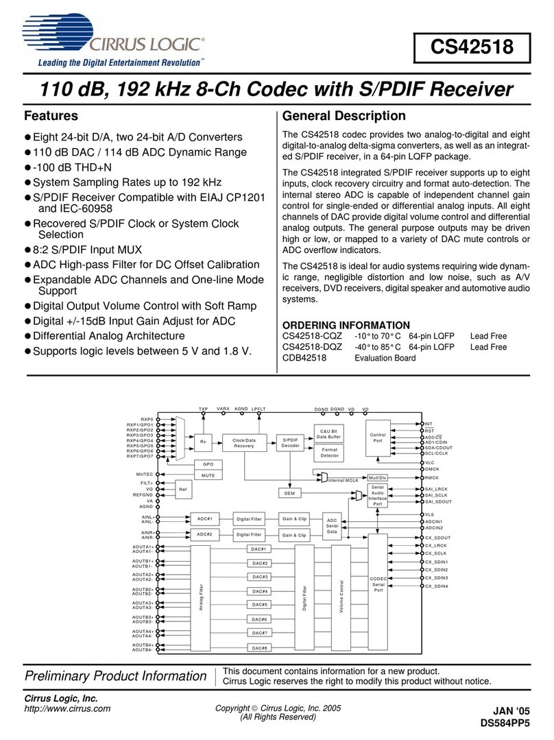
Cirrus Logic
Cirrus Logic CS42518 User manual
Cirrus Logic
Cirrus Logic CS42526 User manual
Cirrus Logic
Cirrus Logic WM8940 User manual
Cirrus Logic
Cirrus Logic CS42516 User manual
Cirrus Logic
Cirrus Logic CDB4244 User manual
Cirrus Logic
Cirrus Logic CDB42528 User manual
