Cirrus Logic CDB4244 User manual

Copyright Cirrus Logic, Inc. 2011
(All Rights Reserved)
http://www.cirrus.com
Preliminary Product Information This document contains information for a new product.
Cirrus Logic reserves the right to modify this product without notice.
4 In/4 Out Audio CODEC with PCM and TDM Interfaces
DAC Features
Advanced multibit delta-sigma modulator
24-bit resolution
Differential or single-ended outputs
Dynamic range (A-weighted)
– -109 dB differential
– -105 dB single-ended
THD+N
– -90 dB differential
– -88 dB single ended
2 Vrms full-scale output into 3-kAC load
Rail-to-rail operation
ADC Features
Advanced multibit delta-sigma modulator
24-bit resolution
Differential inputs
-105 dB dynamic range (A-weighted)
-88 dB THD+N
2 Vrms full-scale input
System Features
TDM, left justified, and I²S serial inputs and outputs
I²CTM host control port
Supports logic levels between 5 and 1.8 V
Supports sample rates up to 96 kHz
Common Applications
Automotive audio systems
AV, Blu-Ray, and DVD receivers
Audio interfaces, mixing consoles, and effects
processors
General Description
The CS4244 provides four multibit analog-to-digital and
four multi-bit digital-to-analog -converters and is
compatible with differential inputs and either differential
or single-ended outputs. Digital volume control, noise
gating, and muting is provided for each DAC path. A se-
lectable high-pass filter is provided for the 4 ADC inputs.
The CS4244 supports master and slave modes and
TDM, left-justified, and I²S modes.
This product is available in a 40-pin QFN package in
Automotive (-40 °C to +105 °C) and Commercial
(-40 °C to +85 °C) temperature grades. The CDB4244
Customer Demonstration Board is also available for de-
vice evaluation and implementation suggestions. See
“Ordering Information” on page 64 for complete details.
AIN4 (±)
AIN3 (±)
AIN2 (±)
AIN1 (±)
I
2
C Control
Data
Contr ol Port
Level Tr anslator
VL
1.8 to 5.0 VDC
RST
INT
SDOUT1
LDO Analog Supply
2.5 V
VA
5.0 VDC
VDREG
Serial Audio Inter face
SDOUT2
AOUT1 (±)
AOUT2 (±)
AOUT3 (±)
AOUT4 (±)
Serial Clock
In/ Out
Master Clock In
Fr am e Sync
Clock / LRCK
SDIN1SDIN2
Di gi tal Fi l ters
Multi-bit
ADC
Interpolation
Filter
Multi-bit
Modulator s
Channel Volume ,
Mute , Invert ,
Noise Gate
DAC &
Analog
Filters
Master
Volume
Contr ol
MAY ‘11
DS900PP2
CS4244

DS900PP2 2
CS4244
TABLE OF CONTENTS
1. PIN DESCRIPTIONS ............................................................................................................................ 5
1.1 I/O Pin Characteristics ..................................................................................................................... 6
2. TYPICAL CONNECTION DIAGRAM ................................................................................................... 7
3. CHARACTERISTICS AND SPECIFICATIONS ...................................................................................... 8
RECOMMENDED OPERATING CONDITIONS .................................................................................... 8
ABSOLUTE MAXIMUM RATINGS ........................................................................................................ 8
DC ELECTRICAL CHARACTERISTICS ................................................................................................ 9
TYPICAL CURRENT CONSUMPTION ............................................................................................... 10
ANALOG INPUT CHARACTERISTICS (COMMERCIAL GRADE) ...................................................... 11
ANALOG INPUT CHARACTERISTICS (AUTOMOTIVE GRADE) ...................................................... 12
ADC DIGITAL FILTER CHARACTERISTICS ...................................................................................... 14
ANALOG OUTPUT CHARACTERISTICS (COMMERCIAL GRADE) .................................................. 15
ANALOG OUTPUT CHARACTERISTICS (AUTOMOTIVE GRADE) .................................................. 16
COMBINED DAC INTERPOLATION & ON-CHIP ANALOG FILTER RESPONSE ............................. 17
DIGITAL I/O CHARACTERISTICS ...................................................................................................... 18
SWITCHING CHARACTERISTICS - SERIAL AUDIO INTERFACE .................................................... 19
SWITCHING SPECIFICATIONS - CONTROL PORT .......................................................................... 21
4. APPLICATIONS ................................................................................................................................... 22
4.1 Power Supply Decoupling, Grounding, and PCB Layout ............................................................... 22
4.2 Recommended Power-up & Power-down Sequence ..................................................................... 22
4.3 I²C Control Port .............................................................................................................................. 24
4.4 System Clocking ............................................................................................................................ 26
4.5 Serial Port Interface ....................................................................................................................... 28
4.6 Internal Signal Path ....................................................................................................................... 31
4.7 Reset Line ...................................................................................................................................... 42
4.8 Error Reporting and Interrupt Behavior .......................................................................................... 43
5. REGISTER QUICK REFERENCE ........................................................................................................ 46
6. REGISTER DESCRIPTIONS ................................................................................................................ 48
6.1 Device I.D. A–F (Address 01h–03h) (Read Only) ....................................................................... 48
6.2 Revision I.D. (Address 05h) (Read Only) ....................................................................................... 48
6.3 Clock & SP Select (Address 06h) .................................................................................................. 49
6.4 Sample Width Select (Address 07h) .............................................................................................. 50
6.5 Serial Port Control (Address 08h) .................................................................................................. 50
6.6 Serial Port Data Select (Address 09h) ........................................................................................... 51
6.7 ADC Control 1 (Address 0Fh) ........................................................................................................ 52
6.8 ADC Control 2 (Address 10h) ........................................................................................................ 52
6.9 DAC Control 1 (Address 12h) ........................................................................................................ 53
6.10 DAC Control 2 (Address 13h) ...................................................................................................... 53
6.11 DAC Control 3 (Address 14h) ...................................................................................................... 54
6.12 DAC Control 4 (Address 15h) ...................................................................................................... 54
6.13 Volume Mode (Address 16h) ....................................................................................................... 55
6.14 Master and DAC1-4 Volume Control (Address 17h, 18h, 19h, 1Ah, & 1Bh) ................................ 56
6.15 Interrupt Control (Address 1Eh) ................................................................................................... 56
6.16 Interrupt Mask 1 (Address 1Fh) ................................................................................................... 57
6.17 Interrupt Mask 2 (Address 20h) ................................................................................................... 58
6.18 Interrupt Notification 1 (Address 21h) (Read Only) ...................................................................... 58
6.19 Interrupt Notification 2 (Address 22h) (Read Only) ...................................................................... 59
7. ADC FILTER PLOTS ............................................................................................................................ 60
8. DAC FILTER PLOTS ............................................................................................................................ 61
9. PACKAGE DIMENSIONS ................................................................................................................... 63
10. ORDERING INFORMATION .............................................................................................................. 64
11. REVISION HISTORY .......................................................................................................................... 65

DS900PP2 3
CS4244
LIST OF FIGURES
Figure 1. CS4244 Pinout ............................................................................................................................. 5
Figure 2. Typical Connection Diagram ........................................................................................................ 7
Figure 3. Test Circuit for ADC Performance Testing ................................................................................. 13
Figure 4. PSRR Test Configuration ........................................................................................................... 13
Figure 5. Equivalent Output Test Load ..................................................................................................... 16
Figure 6. TDM Serial Audio Interface Timing ............................................................................................ 20
Figure 7. PCM Serial Audio Interface Timing ............................................................................................ 20
Figure 8. I²C Control Port Timing .............................................................................................................. 21
Figure 9. System Level Initialization and Power-Up/Down Sequence ...................................................... 23
Figure 10. DAC DC Loading ..................................................................................................................... 24
Figure 11. Timing, I²C Write ...................................................................................................................... 25
Figure 12. Timing, I²C Read ...................................................................................................................... 25
Figure 13. Master Mode Clocking ............................................................................................................. 27
Figure 14. TDM System Clock Format ...................................................................................................... 28
Figure 15. 32-bit Receiver Channel Block ................................................................................................. 28
Figure 16. Serial Data Coding and Extraction Options within the TDM Streams ...................................... 29
Figure 17. Left Justified Format ................................................................................................................ 30
Figure 18. I²S Format ................................................................................................................................ 30
Figure 19. Audio Path Routing .................................................................................................................. 31
Figure 20. Conventional SDOUT (Left) vs. Sidechain SDOUT (Right) Configuration ............................... 32
Figure 21. DAC1-4 Serial Data Source Selection ..................................................................................... 33
Figure 22. Example Serial Data Source Selection .................................................................................... 34
Figure 23. ADC Path ................................................................................................................................. 35
Figure 24. Single-Ended to Differential Active Input Filter ........................................................................ 36
Figure 25. Single-Ended to Differential Active Input Filter - DC Coupled Input Signal (VA/2 Centered) ... 36
Figure 26. DAC1-4 Path ............................................................................................................................ 37
Figure 27. De-emphasis Curve ................................................................................................................. 38
Figure 28. Passive Analog Output Filter ................................................................................................... 38
Figure 29. Volume Implementation for the DAC1-4 Path .......................................................................... 39
Figure 30. Soft Ramp Behavior ................................................................................................................. 40
Figure 31. Interrupt Behavior and Example Interrupt Service Routine ...................................................... 45
Figure 32. ADC Stopband Rejection ......................................................................................................... 60
Figure 33. ADC Transition Band ............................................................................................................... 60
Figure 34. ADC Transition Band (Detail) ................................................................................................... 60
Figure 35. ADC Passband Ripple ............................................................................................................. 60
Figure 36. ADC HPF (48 kHz) ................................................................................................................... 60
Figure 37. ADC HPF (96 kHz) ................................................................................................................... 60
Figure 38. SSM DAC Stopband Rejection ................................................................................................ 61
Figure 39. SSM DAC Transition Band ...................................................................................................... 61
Figure 40. SSM DAC Transition Band (Detail) .......................................................................................... 61
Figure 41. SSM DAC Passband Ripple .................................................................................................... 61
Figure 42. DSM DAC Stopband Rejection ................................................................................................ 62
Figure 43. DSM DAC Transition Band ...................................................................................................... 62
Figure 44. DSM DAC Transition Band (Detail) .......................................................................................... 62
Figure 45. DSM DAC Passband Ripple .................................................................................................... 62
Figure 46. Package Drawing ..................................................................................................................... 63

DS900PP2 4
CS4244
LIST OF TABLES
Table 1. Speed Modes .............................................................................................................................. 26
Table 2. Common Clock Frequencies ....................................................................................................... 26
Table 3. Master Mode Left Justified and I²S Clock Ratios ........................................................................ 27
Table 4. Slave Mode Left Justified and I²S Clock Ratios .......................................................................... 27
Table 5. Slave Mode TDM Clock Ratios ................................................................................................... 27
Table 6. Soft Ramp Rates ......................................................................................................................... 41
Table 7. Noise Gate Bit Depth Settings .................................................................................................... 42
Table 8. Error Reporting and Interrupt Behavior Details ........................................................................... 43

DS900PP2 5
CS4244
1. PIN DESCRIPTIONS
Figure 1. CS4244 Pinout
Pin Name Pin # Pin Description
SDA 1 Serial Control Data (Input/Output) - Bi-directional data I/O for the I²C control port.
SDINx 2,3 Serial Data Input (Input) - Input channels serial audio data.
FS/LRCK 4 Frame Synchronization Clock/Left/Right Clock (Input/Output) - Determines which channel or
frame is currently active on the serial audio data line.
MCLK 5 Master Clock (Input) -Clock source for the internal logic, processing, and modulators.
SCLK 6 Serial Clock (Input/Output) -Serial Clock for the serial data port.
SDOUT1 7 Serial Data Output 1 (Output) - ADC data output into a multi-slot TDM stream or AIN1 and AIN2
ADC data output in Left Justified and I²S modes.
VL 8 Interface Power (Input) - Positive power for the digital interface level shifters.
GND 9,21 Ground (Input) - Ground reference for the I/O and digital, analog sections.
VDREG 10 Digital Power (Output) - Internally generated positive power supply for digital section.
AINx+ 11,13,15,
17
Positive Analog Input (Input) - Positive input signals to the internal analog to digital converters.
The full scale analog input level is specified in the Analog Input Characteristics tables on pages 11
and 12.
AINx- 12,14,16,
18
Negative Analog Input (Input) - Negative input signals to the internal analog to digital converters.
The full scale analog input level is specified in the Analog Input Characteristics tables on pages 11
and 12.
FILT+ 19 Positive Voltage Reference (Output) - Positive reference voltage for the internal ADCs.
AD0
AD2/SDOUT2
TSTO1
VA
AIN3+
AIN4-
AIN3-
AIN2+
AIN2-
AIN1-
AIN1+
FILT+
SDA
MCLK
SDOUT1
VL
GND
SDIN1
SDIN2
12
11
13
14
15
16
17
18
19
20
29
30
28
27
26
25
24
23
22
21
39
40
38
37
36
35
34
33
32
31
2
1
3
4
5
6
7
8
9
10
AOUT1+
SCLK
VDREG
AOUT2+
AOUT2-
AOUT3+
AOUT3-
AOUT4-
AOUT4+
VBIAS
VREF
VQ
GND
TSTO2
AOUT1-
SCL
FS/LRCK
AD1
INT
RST
AIN4+
Top-Down
(Though Package)
View

DS900PP2 6
CS4244
1.1 I/O Pin Characteristics
Input and output levels and associated power supply voltage are shown in the table below. Logic levels
should not exceed the corresponding power supply voltage.
Notes:
1. Internal connection valid when device is in reset.
2. This pin has no internal pull-up or pull-down resistors. External pull-up or pull-down resistors should
be added in accordance with Figure 2.
VA 20 Analog Power (Input) - Positive power for the analog sections.
VQ 22 Quiescent Voltage (Output)-Filter connection for internal quiescent voltage.
VREF 23 Analog Power Reference (Input) - Return pin for the VBIAS cap.
VBIAS 24 Positive Voltage Reference (Output) - Positive reference voltage for the internal DACs.
AOUTx- 25,27,29,
31
Negative Analog Output (Output) - Negative output signals from the internal digital to analog con-
verters. The full scale analog output level is specified in the Analog Output Characteristics
tables on pages 15 and 16.
AOUTx+ 26,28,30,
32
Positive Analog Output (Output) - Positive output signals from the internal digital to analog con-
verters. The full scale analog output level is specified in the Analog Output Characteristics
tables on pages 15 and 16.
TSTOx 33,34 Test Outputs (Output) - Test outputs. These pins should be left unconnected.
RST 35 Reset (Input) - Applies reset to the internal circuitry when pulled low.
INT 36 Interrupt (Output) - Sent to DSP to indicate an interrupt condition has occurred.
AD2/SDOUT2 37
I²C Address Bit 2 / Serial Data Output 2 (Input/Output) - Sets the I²C address bit 2 at reset. Func-
tions as Serial Data Out 2 for AIN3 and AIN4 ADC data output in Left Justified and I²S modes. High
impedance in TDM mode. See Section 4.3 I²C Control Port for more details concerning this mode of
operation.
AD1 38 I²C Address Bit 1 (Input) - Sets the I²C address bit 1.
AD0 39 I²C Address Bit 0 (Input) - Sets the I²C address bit 0.
SCL 40 Serial Control Port Clock (Input) - Serial clock for the I²C control port.
GND - Thermal Pad - The thermal pad on the bottom of the device should be connected to the ground
plane via an array of vias.
Power Supply Pin Name I/O Driver Internal Connections
(Note 1) Receiver
VL
SCL Input - Weak Pull-down (~500k 5.0 V CMOS, with Hysteresis
SDA Input/Output CMOS/Open
Drain Weak Pull-down (~500k 5.0 V CMOS, with Hysteresis
INT Output CMOS/Open
Drain (Note 2) -
RST Input - (Note 2) 5.0 V CMOS, with Hysteresis
MCLK Input - Weak Pull-down (~500k 5.0 V CMOS, with Hysteresis
FS/LRCK Input/Output 5.0 V CMOS Weak Pull-down (~500k 5.0 V CMOS, with Hysteresis
SCLK Input/Output 5.0 V CMOS Weak Pull-down (~500k 5.0 V CMOS, with Hysteresis
SDOUT1 Output 5.0 V CMOS Weak Pull-down (~500k
SDINx Input - Weak Pull-down (~500k 5.0 V CMOS, with Hysteresis
AD0,1 Input - (Note 2) 5.0 V CMOS
AD2/SDOUT2 Input/Output 5.0 V CMOS (Note 2) 5.0 V CMOS

DS900PP2 7
CS4244
2. TYPICAL CONNECTION DIAGRAM
Figure 2. Typical Connection Diagram
CS4244
AIN4-
AIN3+
AIN2-
AIN3-
VA
FILT+
AIN1+
AIN1-
AIN2+
AIN4+
SDOUT1
VL
GND
FS/LRCK
MCLK
SDIN 2
SDIN 1
SDA
VDREG
SCLK
AD2/ SDOU T2
INT
AOUT1-
TSTO2
AOUT1+
TSTO1
RST
AD0
AD1
SCL
35
AOUT3 -
AOUT4 +
GND
VREF
VQ
VBIAS
AOUT4 -
AOUT2 -
AOUT3 +
AOUT2 +
32 31
+1.8 V to +5 .0 V
0. 1uF
Pull Up or
Down Based
upon Desired
Address
***
0.1 uF
10 uF
Rp (x4)
40 38 37 3639
Digital Signal
Processor
1
3
2
6
4
5
7
8
VL
3334
30
28
27
26
25
22
29
23
0 .1uF 10 uF
+3 .3 V to
+5.0 V
1uF
20
24
10 uF
0 .1uF
10
9
19
21
Analog Output Filter *
Analog Output Filter *
Analog Output Filter *
Analog In put
Filter **
11 12 1413
Analog In put
Filter **
Analog In put
Filter **
Analog In put
Filter **
17 1815 16
Analog Output Filter *
10 uF
****
* See Section 4.6.4
** See Section 4.6.2.2
*** See Section 4.3
**** See Switching Specifications - Control Port

DS900PP2 8
CS4244
3. CHARACTERISTICS AND SPECIFICATIONS
RECOMMENDED OPERATING CONDITIONS
GND = 0 V; all voltages with respect to ground. (Note 3)
Notes: 3. Device functional operation is guaranteed within these limits. Functionality is not guaranteed or
implied outside of these limits. Operation outside of these limits may adversely affect device reliability.
ABSOLUTE MAXIMUM RATINGS
GND = 0 V; all voltages with respect to ground.
WARNING: OPERATION BEYOND THESE LIMITS MAY RESULT IN PERMANENT DAMAGE TO THE DEVICE.
Notes: 4. No external loads should be connected to the VDREG pin. Any connection of a load to this point may
result in errant operation or performance degradation in the device.
5. Any pin except supplies. Transient currents of up to ±100 mA on the analog input pins will not cause
SCR latch-up.
6. The maximum over/under voltage is limited by the input current.
Parameters Symbol Min Typ Max Units
DC Power Supply
Analog Core VA 3.135
4.75
3.3
5
3.465
5.25
V
V
Level Translator VL 1.71 - 5.25 V
Temperature
Ambient Operating Temperature - Power Applied Automotive
Commercial TA
-40
-20
-
-
+105
+85
C
C
Junction Temperature TJ-40 - +150 C
Parameters Symbol Min Max Units
DC Power Supply
Analog Core VA -0.3 5.5 V
Level Translator VL -0.3 5.5 V
VDREG Current (Note 4) IVDREG -10A
Inputs
Input Current (Note 5) Iin -±10mA
Analog Input Voltage (Note 6) VINA - 0.3 VA + 0.4 V
Logic Level Input Voltage (Note 6) VIND -0.3 VL + 0.4 V
Temperature
Ambient Operating Temperature - Power Applied TA-55 +125 °C
Storage Temperature Tstg -65 +150 °C

DS900PP2 9
CS4244
DC ELECTRICAL CHARACTERISTICS
GND = 0 V; all voltages with respect to ground.
Notes:
7. No external loads should be connected to the VDREG pin. Any connection of a load to this point may
result in errant operation or performance degradation in the device.
Parameters Min Typ Max Units
VDREG (Note 7)
Nominal Voltage
Output Impedance
-
-
2.5
0.5
-
-
V
FILT+
Nominal Voltage
Output Impedance
DC Current Source/Sink
-
-
-
VA
23
-
-
-
1
V
k
A
VQ
Nominal Voltage
Output Impedance
DC Current Source/Sink
-
-
-
0.5•VA
77
-
-
-
0
V
k
A

DS900PP2 10
CS4244
TYPICAL CURRENT CONSUMPTION
This table represents the power consumption for individual circuit blocks within the CS4244. CS4244 is configured as
shown in Figure 2 on page 7. VA_SEL = 0 for VA = 3.3 VDC, 1 for VA = 5.0 VDC; FS= 100 kHz; MCLK = 25.6 MHz;
DAC load is 3 k; All input signals are zero (digital zero for SDINx inputs and AC coupled to ground for AINx
inputs) .
Notes:
8. Full-scale differential output signal.
9. Current consumption increases with increasing FSand increasing MCLK. Values are based on FSof
100 kHz and MCLK of 25.6 MHz. Current variance between speed modes is small.
10. PLL is activated by setting the MCLK RATE bit to either 000 (operating in 256x mode) or 001 (operating
in 384kHz).
11. Internal to the CS4244, the analog to digital converters are grouped together in stereo pairs. ADC1 and
ADC2 are grouped together as are ADC3 and ADC4. The ADC group current draw is the current that
is drawn whenever one of these groups become active.
12. To calculate total current draw for an arbitrary amount of ADCs or DACs, the following equations apply:
Total Running CurrentDraw from VA Supply = Power Down Overhead + PLL (If Applicable)+ DAC Current Draw + ADC Current Draw
where
DAC Current Draw = DAC Overhead + (Number of DACs x DAC Channel)
ADC Current Draw = ADC Overhead + (Number of active ADC Groups x ADC Group) + (Number of active ADC Channels x ADC Channel)
and
Total Running Current Draw from VLSupply = PDN Overhead + (Number of active ADC Channels x ADC Channel)
Typical Current [mA]
(unless otherwise noted)
(Note 9), (Note 12)
Functional Block VA/VL iVA iVL
1Reset Overhead
(All lines held static, RST line pulled low.)
5 0.030 0.001
3.3 0.020 0.001
2Power Down Overhead
(All lines clocks and data lines active, RST line pulled high, All PDNx bits set high.)
5 5 0.101
3.3 5 0.101
3PLL(Note 10)
(Current drawn resulting from PLL being active. PLL is active for 256x and 384x)
51 -
3.3 1 -
4DAC Overhead
(Current drawn whenever any of the four DACs are powered up.)
550 -
3.3 45 -
5DAC Channel (Note 8)
(Current drawn per each DAC powered up.)
55 -
3.3 4 -
6ADC Overhead
(Current drawn whenever any of the four ADCs are powered up.)
511 -
3.3 11 -
7ADC Group
(Current drawn due to an ADC “group” being powered up. See (Note 11))
52 -
3.3 2 -
8ADC Channel
(Current drawn per each ADC powered up.)
5 2 0.109
3.3 2 0.066

DS900PP2 11
CS4244
ANALOG INPUT CHARACTERISTICS (COMMERCIAL GRADE)
Test Conditions (unless otherwise specified): Device configured as shown in Section 2. on page 7. Input sine
wave: 1 kHz; VA_SEL = 0 for VA = 3.3 VDC, 1 for VA = 5.0 VDC.; TA= 25 C; Measurement Bandwidth is 20 Hz to
20 kHz unless otherwise specified; Sample Rate = 48 kHz; all Power Down ADCx bits = 0. See (Note 13).
VA, VREF = 3.3 V VA, VREF = 5.0 V
Parameter Min Typ Max Min Typ Max Unit
Dynamic Range
A-weighted
unweighted
95
92
101
98
-
-
99
96
105
102
-
-
dB
dB
Total Harmonic Distortion + Noise
-1 dBFS
-60 dBFS
-
-
-95
-38
-89
-32
-
-
-88
-42
-82
-36
dB
dB
Other Analog Characteristics
Interchannel Gain Mismatch - 0.2 - - 0.2 - dB
Gain Drift - ±100 - - ±100 - ppm/°C
Offset Error (Note 14)
High Pass Filter On
High Pass Filter Off
-
-
0.0001
0.25
-
-
-
-
0.0001
0.25
-
-
% Full Scale
% Full Scale
Interchannel Isolation - 90 - - 90 - dB
Full-scale Input Voltage
(Differential Inputs) 1.58•VA 1.66•VA 1.74•VA 1.58•VA 1.66•VA 1.74•VA Vpp
Input Impedance - 40 - - 40 - k
Common Mode Rejection
(Differential Inputs)
-60- -60- dB
PSRR (Note 15) 1 kHz
60 Hz
-
-
57
57
-
-
-
-
57
57
-
-
dB
dB

DS900PP2 12
CS4244
ANALOG INPUT CHARACTERISTICS (AUTOMOTIVE GRADE)
Test Conditions (unless otherwise specified): Device configured as shown in Section 2. on page 7. Input sine
wave: 1 kHz; VA_SEL = 0 for VA = 3.3 VDC, 1 for VA = 5.0 VDC.; TA= -40 to +105 C; Measurement Bandwidth is
20 Hz to 20 kHz unless otherwise specified; Sample Rate = 48 kHz; all Power Down ADCx bits = 0. See (Note 13).
Notes:
13. Specifications are valid under either of these conditions:
ADCx Common Mode register bit enabled and Enable High-pass Filter register bit enabled.
ADCx Common Mode register bit disabled and Enable High-pass Filter register bit enabled or disabled.
14. AINx+ connected to AINx-.
15. Valid with the recommended capacitor values on FILT+ and VQ. See Figure 4 for test configuration.
VA, VREF = 3.3 V VA, VREF = 5.0 V
Parameter Min Typ Max Min Typ Max Unit
Dynamic Range
A-weighted
unweighted
93
90
101
98
-
-
97
94
105
102
-
-
dB
dB
Total Harmonic Distortion + Noise
-1 dBFS
-60 dBFS
-
-
-95
-38
-87
-30
-
-
-88
-42
-80
-34
dB
dB
Other Analog Characteristics
Interchannel Gain Mismatch - 0.2 - - 0.2 - dB
Gain Drift - ±100 - - ±100 - ppm/°C
Offset Error (Note 14)
High Pass Filter On
High Pass Filter Off
-
-
0.0001
0.25
-
-
-
-
0.0001
0.25
-
-
% Full Scale
% Full Scale
Interchannel Isolation - 90 - - 90 - dB
Full-scale Input Voltage
(Differential Inputs) 1.58•VA 1.66•VA 1.74•VA 1.58•VA 1.66•VA 1.74•VA Vpp
Input Impedance - 40 - - 40 - k
Common Mode Rejection
(Differential Inputs)
-60- -60- dB
PSRR (Note 15) 1 kHz
60 Hz
-
-
60
60
-
-
-
-
60
60
-
-
dB
dB

DS900PP2 13
CS4244
Figure 3. Test Circuit for ADC Performance Testing
Figure 4. PSRR Test Configuration
100 k
4.7 uF
100 k
100 k
470 pF
634
90 .9
Analog Si gnal +
+
-
100 k
4.7 uF
100 k
100 k
470 pF
634
90 .9
Analog Signal -
+
-
VA
VA
2700 pF
CS4244 AINx +
CS4244 AINx -
Operational
Amplifier
OUT
GND
Power DAC
Analog
Out
GND
PWR
DUT
+Vcc
+Vcc
+
-
OUT
Test Equipment
Analog Generator Analyzer
-Vcc Digital
Out
+
-+
-
+
-

DS900PP2 14
CS4244
ADC DIGITAL FILTER CHARACTERISTICS
Test Conditions (unless otherwise specified): Device configured as shown in Section 2. on page 7. Input sine
wave: 1 kHz; VA_SEL = 0 for VA = 3.3 VDC, 1 for VA = 5.0 VDC.; TA= -40 to +105 C; Measurement Bandwidth is
20 Hz to 20 kHz unless otherwise specified. See filter plots in Section 7. on page 60.
Note:
16. Response is clock-dependent and will scale with Fs.
17. The ADC group delay is measured from the time the analog inputs are sampled on the AINx pins to
the FS/LRCK transition (rising or falling) after the last bit of that (group of) sample(s) has been
transmitted on SDOUTx.
18. The amount of time from input of half-full-scale step function until the filter output settles to 0.1% of
full scale.
Parameter (Note 16) Min Typ Max Unit
Passband (Frequency Response) to -0.1 dB corner 0 - 0.4535 Fs
Passband Ripple -0.09 - 0.17 dB
Stopband 0.6 - - Fs
Stopband Attenuation 70 - - dB
Single-Speed Mode
ADC Group Delay (Note 17) - 9.5/Fs - s
High-Pass Filter Characteristics (48 kHz Fs)
Frequency Response -3.0 dB
-0.13 dB
-
-
2
11
-
-
Hz
Hz
Phase Deviation @ 20 Hz - 10 - Deg
Passband Ripple -0.09 - 0.17 dB
Filter Settling Time (Note 18) -25000/Fs 0s
Double-Speed Mode
ADC Group Delay (Note 17) - 9.5/Fs - s
High-Pass Filter Characteristics (96 kHz Fs)
Frequency Response -3.0 dB
-0.13 dB
-
-
4
22
-
-
Hz
Hz
Phase Deviation @ 20 Hz - 10 - Deg
Passband Ripple -0.15 - 0.17 dB
Filter Settling Time (Note 18) -25000/Fs 0s

DS900PP2 15
CS4244
ANALOG OUTPUT CHARACTERISTICS (COMMERCIAL GRADE)
Test Conditions (unless otherwise specified). Device configured as shown in Section 2. on page 7. VA_SEL = 0 for
VA = 3.3 VDC, 1 for VA = 5.0 VDC.; TA= 25 C; Full-scale 1 kHz input sine wave; Sample Rate = 48 kHz; Mea-
surement Bandwidth is 20 Hz to 20 kHz; Specifications apply to all channels unless otherwise indicated; all Power
Down DACx bits = 0. See (Note 20) on page 16.
VA, VREF= 3.3 V
(Differential/Single-ended)
VA, VREF= 5.0 V
(Differential/Single-ended)
Parameter Min Typ Max Min Typ Max Unit
Dynamic Performance
Dynamic Range
18 to 24-Bit A-weighted
unweighted
16-Bit A-weighted
unweighted
100/96
97/93
89
86
106/102
103/99
95
92
-
-
-
-
103/99
100/96
89
86
109/105
106/102
95
92
-
-
-
-
dB
dB
dB
dB
Total Harmonic Distortion + Noise - -90/-88 -84/-82 - -90/-88 -84/-82 dB
Full-scale Output Voltage 1.48•VA/
0.74•VA
1.56•VA/
0.78•VA
1.64•VA/
0.82•VA
1.48•VA/
0.74•VA
1.56•VA/
0.78•VA
1.64•VA/
0.82•VA
Vpp
Interchannel Isolation (1 kHz) - 100 - - 100 - dB
Interchannel Gain Mismatch - 0.1 0.25 - 0.1 0.25 dB
Gain Drift - ±100 - - ±100 - ppm/°C
AC-Load Resistance (RL)(Note 20) 3- -3--k
Load Capacitance (CL)(Note 20) - - 100 - - 100 pF
Parallel DC-Load Resistance(Note 21) 10 - - 10 - - k
Output Impedance - 100 - - 100 -
PSRR (Note 22) 1 kHz
60 Hz
-
-
60
60
-
-
-
-
60
60
-
-
dB
dB

DS900PP2 16
CS4244
ANALOG OUTPUT CHARACTERISTICS (AUTOMOTIVE GRADE)
Test Conditions (unless otherwise specified): Device configured as shown in Section 2. on page 7. VA_SEL = 0 for
VA = 3.3 VDC, 1 for VA = 5.0 VDC.; TA= -40 to +105 C; Full-scale 1 kHz input sine wave; Sample Rate = 48 kHz;
Measurement Bandwidth is 20 Hz to 20 kHz; Specifications apply to all channels unless otherwise indicated; all
Power Down DACx bits = 0. See (Note 20).
Notes:
19. One LSB of triangular PDF dither added to data.
20. Loading configuration is given in Figure 5 below.
Figure 5. Equivalent Output Test Load
21. Parallel combination of all DAC DC loads. See Section 4.2.3.
22. Valid with the recommended capacitor values on FILT+ and VQ. See Figure 4 for test configuration.
VA, VREF= 3.3 V
(Differential/Single-ended)
VA, VREF= 5.0 V
(Differential/Single-ended)
Parameter Min Typ Max Min Typ Max Unit
Dynamic Performance
Dynamic Range
18 to 24-Bit A-weighted
unweighted
16-Bit A-weighted
unweighted
98/94
95/91
87
84
106/102
103/99
95
92
-
-
-
-
101/97
98/94
87
84
109/105
106/102
95
92
-
-
-
-
dB
dB
dB
dB
Total Harmonic Distortion + Noise - -90/-88 -82/-80 - -90/-88 -82/-80 dB
Full-scale Output Voltage 1.48•VA/
0.74•VA
1.56•VA/
0.78•VA
1.64•VA/
0.82•VA
1.48•VA/
0.74•VA
1.56•VA/
0.78•VA
1.64•VA/
0.82•VA
Vpp
Interchannel Isolation (1 kHz) - 100 - - 100 - dB
Interchannel Gain Mismatch - 0.1 0.25 - 0.1 0.25 dB
Gain Drift - ±100 - - ±100 - ppm/°C
AC-Load Resistance (RL)(Note 20) 3--3- -k
Load Capacitance (CL)(Note 20) - - 100 - - 100 pF
Parallel DC-Load Resistance(Note 21) 10 - - 10 - - k
Output Impedance - 100 - - 100 -
PSRR (Note 22) 1 kHz
60 Hz
-
-
60
60
-
-
-
-
60
60
-
-
dB
dB
AOUTx
GND
22 µF
V
OUT
RLCL

DS900PP2 17
CS4244
COMBINED DAC INTERPOLATION & ON-CHIP ANALOG FILTER RESPONSE
Test Conditions (unless otherwise specified): VA_SEL = 0 for VA = 3.3 VDC, 1 for VA = 5.0 VDC. The filter charac-
teristics have been normalized to the sample rate (FS) and can be referenced to the desired sample rate by multi-
plying the given characteristic by FS.
Notes:
23. Response is clock-dependent and will scale with FS.
24. For Single-Speed Mode, the measurement bandwidth is 0.5465 FSto 3 FS.
For Double-Speed Mode, the measurement bandwidth is 0.577 FSto 1.4 FS.
25. The DAC group delay is measured from the FS/LRCK transition (rising or falling) before the first bit of
a (group of) sample(s) is transmitted on the SDINx pins to the time it appears on the AOUTx pins.
Parameter Min Typ Max Unit
Single-Speed Mode
Passband (Note 23) to -0.05 dB corner
to -3 dB corner
0
0
-
-
0.4780
0.4996
FS
FS
Frequency Response 20 Hz to 20 kHz -0.01 - +0.12 dB
StopBand 0.5465 - - FS
StopBand Attenuation (Note 24) 102 - - dB
DAC1-4 Group Delay (Note 25) -11/Fs-s
Double-Speed Mode
Passband (Note 23) to -0.1 dB corner
to -3 dB corner
0
0
-
-
0.4650
0.4982
FS
FS
Frequency Response 20 Hz to 20 kHz -0.05 - +0.2 dB
StopBand 0.5770 - - FS
StopBand Attenuation (Note 24) 80 - - dB
DAC1-4 Group Delay (Note 25) -7/Fs-s

DS900PP2 18
CS4244
DIGITAL I/O CHARACTERISTICS
Parameters Symbol Min Typ Max Units
High-Level Input Voltage (all input pins except RST)(%ofVL)
(VL=1.8V) VIH 75% - - V
High-Level Input Voltage (all input pins except RST)(%ofVL)
(VL=2.5V,3.3V,or5V) VIH 70% - - V
Low-Level Input Voltage (all input pins except RST)(%ofVL)V
IL --30%V
High-Level Input Voltage (RST pin) VIH 1.2 - - V
Low-Level Input Voltage (RST pin) VIL --0.3V
High-Level Output Voltage at Io=2mA (%ofVL) V
OH 80% - - V
Low-Level Output Voltage at Io=2mA (%ofVL) V
OL --20%V
Input Leakage Current Iin --±10A
Input Capacitance - 8 - pF

DS900PP2 19
CS4244
SWITCHING CHARACTERISTICS - SERIAL AUDIO INTERFACE
VA_SEL = 0 for VA = 3.3 VDC, 1 for VA = 5.0 VDC.
Notes:
26. After applying power to the CS4244, RST should be held low until after the power supplies and MCLK
are stable.
27. MCLK must be synchronous to and scale with FS.
28. The SCLK frequency must remain less than or equal to the MCLK frequency. For this reason, SCLK
may range from 256x to 512x only in single speed mode. In double speed mode, 256x is the only ratio
supported.
29. The MSB of CH1 is always aligned with the second SCLK rising edge following FS/LRCK rising edge.
30. Where “n” is equal to the MCLK to LRCK ratio (set by the Master Clock Rate register bits), i.e. in 256x
mode, n = 256, in 512x mode, n = 512, etc.
Parameters Symbol Min Max Units
RST pin Low Pulse Width (Note 26) 1-ms
MCLK Frequency (Note 27) 7.68 25.6 MHz
MCLK Duty Cycle 45 55 %
SCLK Duty Cycle 45 55 %
Input Sample Rate (FS/LRCK pin) Single-Speed Mode
Double-Speed Mode
FS
FS
30
60
50
100
kHz
kHz
SCLK Falling Edge to SDOUTx Valid (VL = 1.8 V) tdh2 -31ns
SCLK Falling Edge to SDOUTx Valid (VL = 2.5 V) tdh2 -22ns
SCLK Falling Edge to SDOUTx Valid (VL = 3.3 V or 5 V) tdh2 -17ns
TDM Slave Mode
SCLK Frequency (Note 28) 256x 512x FS
FS/LRCK High Time Pulse (Note 29) tlpw 1/fSCLK (n-1)/fSCLK
(Note 30)
ns
FS/LRCK Rising Edge to SCLK Rising Edge tlcks 5-ns
SDINx Setup Time Before SCLK Rising Edge tds 3-ns
SDINx Hold Time After SCLK Rising Edge tdh1 5-ns
PCM Slave Mode
SCLK Frequency 32x 64x FS
FS/LRCK Duty Cycle 45 55 %
FS/LRCK Edge to SCLK Rising Edge tlcks 5-ns
SDINx Setup Time Before SCLK Rising Edge tds 3-ns
SDINx Hold Time After SCLK Rising Edge tdh1 5-ns
PCM Master Mode
SCLK Frequency 64x 64x FS
FS/LRCK Duty Cycle 45 55 %
FS/LRCK Edge to SCLK Rising Edge tlcks 5-ns
SDINx Setup Time Before SCLK Rising Edge tds 5-ns
SDINx Hold Time After SCLK Rising Edge
(VL=1.8V) tdh1 11 - ns
SDINx Hold Time After SCLK Rising Edge
(VL=2.5V,3.3V,or5V) tdh1 10 - ns

DS900PP2 20
CS4244
Figure 6. TDM Serial Audio Interface Timing
SDOUT1
(output )
SDINx
(input )
t
ds
SCLK
(input )
FS/LRCK
(input )
MSB
t
dh1
MSB-1
t
lcks
t
dh2
MSB MSB-1
t
dh2
t
LPW
~
~
~
t
ds
MSB
t
dh1
t
dh2
MSB-1
t
lcks
FS/LRCK
(input /output )
SCLK
(input /output )
SDINx
(input)
SDOUTx
(output)
MSB MSB-1
Figure 7. PCM Serial Audio Interface Timing
Table of contents
Other Cirrus Logic Conference System manuals
Cirrus Logic
Cirrus Logic WM8940 User manual
Cirrus Logic
Cirrus Logic CS42518 User manual
Cirrus Logic
Cirrus Logic CS4265 User manual
Cirrus Logic
Cirrus Logic CS42L42 User manual
Cirrus Logic
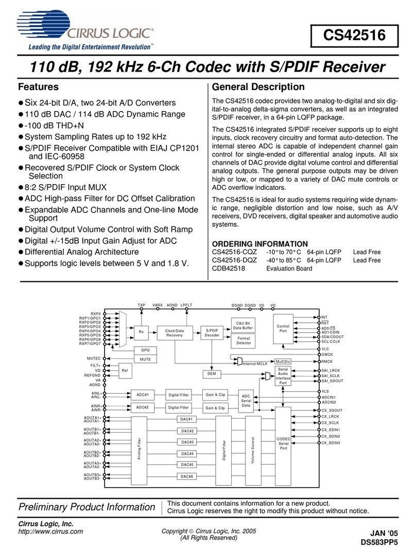
Cirrus Logic CS42516 User manual
Cirrus Logic
Cirrus Logic CDB42528 User manual
Cirrus Logic
Cirrus Logic CS42526 User manual
Popular Conference System manuals by other brands
Sena
Sena 10U for Shoei J-Cruise quick start guide
Bell System
Bell System Com Key 416 Identification, Installation, Connection, Operation, and Maintenance Customer Equipment
Yealink
Yealink CPN10 quick start guide
CMX
CMX UHF-300 Operation manual
PictureTel
PictureTel LIVE50 installation guide
Shure
Shure CU 6110 user manual
