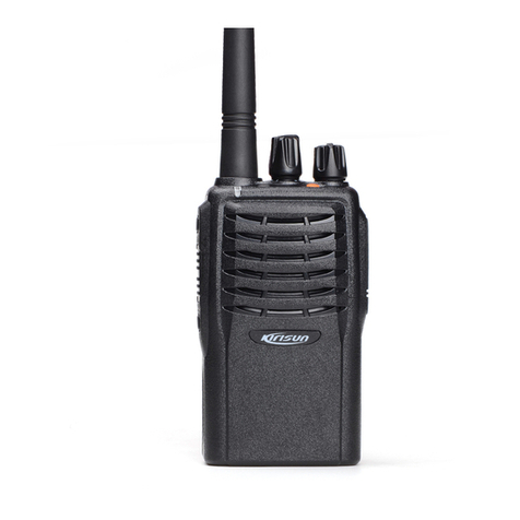
Covalue DR6000-1 User manual

136 to 174MHz,The frequency c
1
Circuit Description
1 Frequency configuration
The reference frequency of frequency synthesizer is provided by 16.8MHz crystal oscillator X1 TCXO.
The receiver adopts quadric mixing mode. The first IF is 49.95MHz, and the second IF is 450kHz. The
first local oscillation signal of the receiver is produced by frequency synthesizer and the second local
oscillation signal selects the 4rd harmonics of 16.8MHz of crystal oscillator X1 TCXO. The signal of
transmitter is produced by frequency synthesizer directly.
Figure 1 Frequency configuration
2 Receiver(Rx)
The receiver is double conversion superheterodyne,designed to operate in the frequency range of
onfiguration in Fig 1.1
Figure 2 Receiver section configuration
Front End of Receiver
Signals from the antenna are filtered by BPF via RX/TX switch (D101 D102 and D103). After being
filtered out the useless out-of-band signals, the signals are amplified by LNA consisting of Q203 and
external components.
Signals from LNA are filtered again by BPF before entering the 1st mixer (Q202).

2
The PWM wave is output by MCU composed of 58 foot and then commutated to adjustable voltage after
filtering to change the capacity of varactor diode D905 D203 D202 and D204 to control the center
frequency of BPF.
1st mixer
The first IF (49.95MHz) signal is produced after mixing of the receiving signal from LNA and the 1st local
oscillation signal from frequency synthesizer. The first IF signal is filtered out adjacent channel and other
useless signals by crystal filter (XF201).
IF Circuit
The 1st IF signal from crystal filter is amplified by the first IF amplifier (Q201) before processing of IC in
IF( IC200,NJM2591V).
IF IC consists of the 2nd mixer, 2nd local oscillation, IF amplifier, limiter, frequency discriminator and noise
amplifier.
Frequency (16.8MHz) produced by TCXO(X1) is amplified and then selects 3rd harmonics (51.4MHZ) as
the second local oscillator signal source. The second IF signals (450kHz) are generated after signals
mixing of the second local oscillation (51.4MHz) and the first IF (49.95MHz) in IC200. Audio signals are
demodulated and outputted by IC200 after the second IF signals are amplified and limited in IC200 and
then filtered by ceramic filter(450kHz).
Figure 3 Schematic Diagram for IF System
Receiving Audio Signal Processing:

3
The audio processing circuit of receiver consists of IC300. Voice signals from IC300 are sent to IC301
(CTCSS signaling filter circuit.
Squelch Circuit
Part of the AF signal from the IC200 enters the FM IC again,and the noise component is amplified
and rectified by a filter and an amplifier to produce a DC voltage corresponding to the noise level.
The DC signal from the FM IC goes to the analog port of the microprocessor(IC403).IC403
determines whether to output sounds from the speaker by checking whether the input voltage is higher
or lower than the preset value.
To output sounds from the speaker,IC403 sends a high signal to the MUTE and AFCO lines and turns
IC302 on through Q302 Q304 and Q305.
Audio Power Amplification
The audio power amplifying circuit consists of IC302 and the peripheral components.
The signals are amplified by audio power amplifier to drive the speaker after collecting the receiving
audio signals, voice signals and warning tone signals. The warning tone has no volume limitation.
When AFCO is high level, Q304 is on, IC302 begins to work and the speaker sounds. Speaker
Impedance: 16ohm
CTCSS Signal filtering
The audio signals after demodulation in IC200 may contain CTCSS (continuous tone control squelch
system) or DCS(digital squelch)signals. The spectrum component of CTCSS/DCS is 67 to 250Hz. The
filtering circuit composed of IC301 can filter out signals except CTCSS/DCS spectrum, which makes
MCU decode the CTCSS/DCS more accurately.
3Transmitter (Tx)
Transmitter Power Amplifier
Figure 4 Schematic Diagram for Power Amplifier and Antenna Switch
The modulated RF signals from VCO are amplified by Q101 and Q105 before the power amplification
in Q107.
Gate bias of Q105 and Q107 is controlled by APC circuit, so the output power of transmitter can be
controlled conveniently by changing the gate bias voltage.

4
APC(Automatic Power Control)
Figure 5 Schematic Diagram for APC Circuit
R130 R131 and R132 are power amplification current detector, IC100A is power amplification current
sampling amplifier and IC00B is power comparison amplifier.
The power amplification current and IC100A output will increase with oversized output power of
transmitter. When the output voltage of IC100B decreases, the bias voltage of Q105 and Q107 will
decrease, finally the output power of transmitter will decrease or vice versa. Thus, the output power of
transmitter will keep stable under any different working condition.
MCU can set the power by changing the voltage input to IC100B.
Audio Signal Processing of Transmitter
Figure 6 Schematic Diagram for Audit Circuit of Receiver
The audio signal processing circuit of Transmitter consists of IC601 and IC609. Voice signals from
MIC are sent to VCO for modulation together with CTCSS/DCS after amplification, limitation and filtering.
IC609 is a bais band processor.
AGC circuit consists of D601, D602 and Q602,Q603. The signal amplitude is reduced to ensure no
distortion in case of oversized MIC signal.
Q601, the power switch of voice processing circuit, controlled by MCU, will give power supply to IC601
only during transmission.
J501 is the socket for external MIC, and the internal MIC will disconnect automatically when using

5
external MIC, but the internal PTT is still effective.
4 PLL Frequency Synthesizer
Figure 7 Schematic Diagram for Frequency Synthesizer
The DR6000-2 adopts PLL frequency synthesizer.
Frequency synthesizer consists of reference oscillator, voltage controlled oscillator (VCO),
programmable frequency divider (PFD), phase comparator and low pass filter (LPF).
RX VCO Unit consists of Q3 D1 D3 L13 C34 C38 C39 and C42.
TX VCO Unit consists of Q4 D2 D4 L14 C35 C41 C44 and C45,D5 is the modulation circuit of VCO.
IC607 (SKY72310) is PLL integrated circuit and contains programmable parametric frequency divider
(PPFD), programmable frequency divider (PFD), phase comparator and charge pump, etc.
Low pass filter consists of R5 R7 R9 R10 C12 C15 and C18.
Reference frequency is provided by X1 (TCXO, 16.8MHz).
Reference frequency of TCXO (Temperature-controlled Crystal Oscillator) is divided by PPFD in IC607
to produce reference frequency of 5kHz or 6.25kHz (controlled by MCU based on the set channel
frequency).
The oscillation frequency of VCO is compared with reference frequency to produce error signal after
divided by PFD in IC607. The error signal is filtered by low pass filter before changing the VCO
frequency to the set value in VCO (it is locking).
N=F
VCO/FR
N:Division Frequency
F
VCO:VCO Oscillation Frequency
FR:Reference Frequency
Lock lost detection: When PLL is out of lock, IC pin4 will output low level signal to MCU,and then MCU
prohibit transmitter from transmitting with a warning tone.
Q8, the power filter, can provide PLL with more purified power to reduce the noise of frequency

6
synthesizer.
5 Base Band Processor
HR_C5000-1 (IC609) is a low power high performance base band processor supporting Tier 1 and
Tier 2 of the DMR protocol. it completes the entire physical layer and data link layer, and voice
processing part of the call control layer of DMR compliant with ETSI TS 102 361.
Figure 8 Base Band Processor
6Voice Circuit:
The station is equipped with Voice Prompt Function, which is very useful during night or under dark
condition.
The speaker will voice the current channel number when changing the channel every time because of
the voice memory chip (IC613), which stores channel voice prompts. It will repeat the current channel
number once pressing “Voice Prompts”.
The speaker will voice the current channel number under standby state if the Voice Prompt Function is
set. Press “Voice Prompts” for reset to switch voice types. Press “Voice Prompts” repeatedly for power
connection, then the voice types will be switched in circle in the order of “Chinese male voice—English
male voice—Chinese female voice—English female voice—no prompts”.
7 Power Supply:
The station use lithium battery (7.4V, 1700mAh), while transmitter amplifier circuit (Q105 Q107) and
receiver audio amplifier (IC302) use battery directly for power supply, and other circuits use regulated
voltage (5V and 3.3V).
IC602:5C (controlled by MCU) (5V LDO)
IC603:5M 5R (controlled by MCU) (5V LDO)

7
IC604:5T (controlled by MCU) (5V LDO)
IC605:3.3V DC/DC
IC618:3.3V LDO, is the supply power of frequency synthesizer
8 MCUUnit:
Figure 9 Schematic Diagram for MCU Unit
MCU Unit controls the operation of every unit to realize all functions of the DR6000-2.
Communication with external PC
State data access
Control PLL for the generation, receiving and transmitting of local oscillation frequency
Access to the current channel state
Control LED status indicator
Control power supplied condition of every unit
Detect action of every function key
Produce CTCSS signal
Produce DCS signal
Produce power controlled signal
Finish CTCSS decoding
Finish DCS decoding
Squelch detection and control
Control voice prompt content

8
Memory (FLASH)
Channel data, CTCSS/DCS data and other function setting data and parameter adjustment data.
CTCSS/DCS signal coding and decoding:
CTCSS/DCS signals from MCU are sent to TCXO for modulation respectively .
CTCSS/DCS signals from receiver are sent to MCU(pin 25) for decoding, and then MCU test if there
are CTCSS/DCS signals with the same setting of the station to decide whether open the speaker or
not.
CTCSS (continuous tone control squelch system, hereinafter referred to as CTCSS), is a kind of
squelch control system with modulation on carrier and continuous sub-audio signals as pilot tone. If
CTCSS function is set, the call is available only at the same CTCSS frequency of both receiving and
transmitting parties to avoid the disturbance of other signals.
The station has 39 groups of standard CTCSS frequency for your selection, such as Table 1.
CTCSS signals produced by MCU are sent to TCXO for modulation.
Table 1 CTCSS Frequency Table
No. Frequency
[Hz] No. Frequency
[Hz] No. Frequency
[Hz] No. Frequency
[Hz]
1 67.0 11 94.8 21 131.8 31 186.2
2 69.3 12 97.4 22 136.5 32 192.8
3 71.9 13 100.0 23 141.3 33 203.5
4 74.4 14 103.5 24 146.2 34 210.7
5 77.0 15 107.2 25 151.4 35 218.1
6 79.7 16 110.9 26 156.7 36 225.7
7 82.5 17 114.8 27 162.2 37 233.6
8 85.4 18 118.8 28 167.9 38 241.8
9 88.5 19 123.0 29 173.8 39 250.3
10 91.5 20 127.3 30 179.9
DCS signaling:
DCS (Digital code squelch), is a kind of continuous digital code modulated on carrier with voice signal
and used for squelch control. If DCS function is set, the speaker is available only when receiving the
same DCS code to avoid the disturbance of useless signals.
The station has 83 kinds of standard codes including positive and inverse code for your selection, such
as Table 2.
DCS signals produced by MCU (PWM waveform) are sent to TCXO for modulation.
CTCSS/DCS signals from receiver are sent to MCU for decoding, and then MCU test if there are DCS
codes with the same setting of the station to decide whether open the speaker or not.
Table 2 DCS Coding Schedule
023 114 174 315 445 631

9
025 115 205 331 464 632
026 116 223 343 465 654
031 125 226 346 466 662
032 131 243 351 503 664
043 132 244 364 506 703
047 134 245 365 516 712
051 143 251 371 532 723
054 152 261 411 546 731
065 155 263 412 565 732
071 156 265 413 606 734
072 162 271 423 612 743
073 165 306 431 624 754
074 172 311 432 627
9 Description of Semiconductor Devices
The distribution of each pin goes as the table 3.
Table 3---Definition of CPU Base Pin:
Pin Type Pin Name Port Name Function
1 O PE2 FLASH_CS SPI Flash Chip Select
2 O PE3 FLASH_SCLK/
LCD_DB6 SPI Flash Serial Clock/
LCD_DB6(multiplexing)
3 I PE4 FLASH_SDO SPI Flash Serial Data
4 O PE5 FLASH_SDI/
LCD_DB7 SPI Flash Serial Data Output(MCU)/
LCD_DB7(multiplexing)
5 O PE6 DMR_SLEEP DMR POWERDOWN(High Active)
6 S VBAT VBAT Connected to VDD
7 O PC13 TX_LED TX_LED(High Active)
8 O PC14 RX_LED RX LED(High Active)
9 O PC15 LAMP Keyboard Lamp(HighActive)
10 S VSS_5 VSS_5 Connected to VSSA.
11 S VDD_5 VDD_5 Connected to 3.3V.
12 I OSC_IN OSC_IN 8MHz Crystal Input
13 O OSC_OUT OSC_OUT 8MHz Crystal Output
14 I RESET RESET Reset Input(Low Active)
15 I PC0/EXTI0
TIME_SLOT_INTE
R DMR TIME_SLOT Interrupt
16 I PC1/EXTI1 SYS_INTER DMR SYS Interrupt
17 I PC2/EXTI2 RF_TX_INTER DMR RF_TX中Interrupt
18 I PC3/EXTI3/
AD123_IN13 RF_RX_INTER DMR RF_RX Interrupt
19 S VDD VDD Connected to 3.3V。

10
20 S VSS VSS Connected to VSSA
21 S VREF+ VREF+ Connected to 3.3V.
22 S VDDA VDDA Connected to 3.3V.
23 I PA0/
ADC123_IN0 MANDOWN MANDOWN Input;
24 I PA1/
ADC123_IN1 BATT Battery Input;
25 I PA2/
ADC123_IN2 QT/DQT_IN CTCSS/DCS Input
26 I PA3/
ADC123_IN3 VOX VOX Input
27 S VSS_4 VSS_4 Connected to VSSA
28 S VDD_4 VDD_4 Connected to 3.3V.
29 O PA4/
DAC_OUT1 APC/TV APC/TV D/A Output
30 O PA5/
DAC_OUT2 MOD2_BIAS TCXO Frequency D/AAdjust
31 I PA6/
ADC12_IN6 POWER_DET Power Detect(High Active)
32 O PA7 POWER_C Power Control(High Active)
33 O PC4 RF_APC_SW RF Amplifier Switch(HighActive)
34 O PC5 5TC 5T Power Control(High Active)
35 I PB0/
ADC12_IN8 RSSI RSSI Detect Input
36 I PB1/
ADC12_IN9 BUSY Carrier Detect Input
37 I/O PB2/BOOT1 FM_SW FM Receive IF Switch(High Active)
38 O PE7 FM_MUTE FM RX Mute(High Active)
39 O PE8 VCOVCC_SW RXVCO/TXVCO Control(High for RX)
40 O PE9 DMR_SW DMR Receive IF Switch(High Active)
41 I PE10 VOL_MAX Max Volume Control(HighActive)
42 O PE11 EXT_PTT Ext PTT Input
43 I PE12 PTT_KEY PTT Input
44 I PE13 ALARM_KEY Top Key Input
45 I PE14 ENCODE_IN0 Channel Encode IN0
46 I PE15 ENCODE_IN1 Channel Encode IN1
47 I PB10 ENCODE_IN2 Channel Encode IN2
48 I PB11 ENCODE_IN3 Channel Encode IN3
49 S VCAP_1 VCAP_1 Connect a Capacitor to Ground
50 S VDD_1 VDD_1 Connected to 3.3V。
51 O PB12/
SPI2_NSS DMR_CS C5000 Chip Select

11
52 O PB13/
SPI2_SCK DMR_SCLK C5000 Serial Clock Output(From MCU)
53 I PB14/
SPI2_MISO DMR_SDO C5000 Serial Data Input
54 O PB15/
SPI2_MOSI DMR_SDI C5000 Serial Data Output
55 I PD8 PLL_LD PLL Lock Detect(High Active)
56 O PD9 PLL_CS PLL Chip Select
57 O PD10 PLL_DAT PLL DATA Output
58 O PD11 PLL_CLK PLL Clock Output
59 O PD12 LCD_RES LCD_RES
60 O PD13 LCD_A0 LCD_A0
61 O PD14 LCD_CS1 LCD_CS1
62 O PD15 FL_C Fast Lock Switch Control(HighActive)
63 O
PC6/TIM8_C
H1 FAST_LOCK Fast Lock PWM Output
64 O
PC7/TIM8_C
H2 CTC/DCS_OUT CTCSS/DCS TCXO Output
65 O
PC8/TIM8_C
H3 BEEP BEEP/ALARM/DTMF Output
66 O PC9 5RC 5R Power Switch Control(HighActive)
67 O PA8 SAVE 5C Power Switch Control(High Active)
68 I PA9/
USART1_TX SD1_KEY Side Key 1 Input
69 I PA10/
USART1_RX SD2_KEY Side Key 2 Input
70 I/O
PA11/USBD
M USBD- USB DM
71 I/O
PA12/USBD
P USBD+ USB DP
72 I/O
JTMS-SWDI
O/
PA13
SWDIO/
WORN_SW Wide/Narrow Band Control(High for Wide )
73 S VCAP_2 VCAP_2 Connect a Capacitor to Ground
74 S VSS_2 VSS_2 Connect to Ground
75 S VDD_2 VDD_2 Connect to 3.3V。
76 I/O
JTCK-SWCL
K/
PA14
SWCLK/
MANDOWN_SW MANDOWN Power Switch(High Active)
77 O PA15/
I2S3_WS I2S_FS DMR I2S_FS
78 O PC10/
I2S3_CK I2S_CK DMR I2S_CK
79 O PC11/ I2S_RX DMR I2S_RX

12
I2S3ext_SD
80 I PC12/
I2S3_SD I2S_TX DMR I2S_TX
81 I/O PD0 K2 Key Board K2 Input
82 I/O PD1 K3 Key Board K3 Input
83 I/O PD2 K4 Key Board K4 Input
84 I/O PD3 K5 Key Board K5 Input
85 I/O PD4 K6 Key Board K6 Input
86 I/O PD5 K7 Key Board K7 Input
87 I/O PD6 K8 Key Board K8 Input
88 O PD7 V_CS DMR V_CS
89 O PB3/
SPI3_SCK V_SCLK DMR V_SCLK
90 I PB4/
SPI3_MISO V_SDO DMR V_SDO
91 O PB5/
SPI3_MOSI V_SDI DMR V_SDI
92 O PB6 SPK_C Speaker Output Control(High Active)
93 O PB7 AFCO Audio Amplifier Control(High Active)
94 I BOOT0 BOOT0 Connect a 10K resistor to Ground
95 O PB8/
I2C1_SCL SCL Software Control Watch Dog Serial Clock
96 O PB9/
I2C1_SDA SDA Software Control Watch Dog Serial Data
97 O PE0 MICPWR_C MIC Power Switch(HighActive)
98 O PE1 K1 Key Board K2 Input
99 S VSS_3 VSS_3 Connect to Ground
100 S VDD_3 VDD_3 Connect to 3.3V。
Table 4 Functional description of semiconductor device
Item Model Function Description
IC1 SKY72310 Frequency Synthesizer
IC100 NJM2904 APC, Voltage Comparison, Driving
IC200 NJM2591V Receiver 2nd Local Oscillation, 2nd IF Amplification, Limitation, Demodulation, Noise
Amplification
IC300 NJM2902V Receiver demodulated signal Amplification, Filtering
IC601 TA75W01FU MIC Amplification
IC302 TDA2822D Audio Frequency Power Amplification
IC613 W25Q80 FLASH, Channel Frequency Data Storage, Function Setting Parameter, Debug

13
Mode Parameter
IC614 STM32F405VGT6 MCU
IC615 PST9124NR MCU Reset Circuit
IC609 HR_C5000-1 Base Band Processor
IC619 UPB1509BV UPB1509GV is a divide by 2, 4, 8 prescaler IC for portable radio or cellular
telephone applications.
Other manuals for DR6000-1
2
Table of contents
Other Covalue Two-way Radio manuals
Covalue
Covalue DR7800-2 User manual
Covalue
Covalue DR6000 User manual
Covalue
Covalue CU600-2 User manual
Covalue
Covalue DR5500-1 User manual
Covalue
Covalue CU500-1 User manual
Covalue
Covalue DP7000-2 User manual
Covalue
Covalue CU780-2 Quick start guide

Covalue
Covalue CU500-2 User manual
Covalue
Covalue DR5810-2 User manual
Covalue
Covalue CU780 User manual
