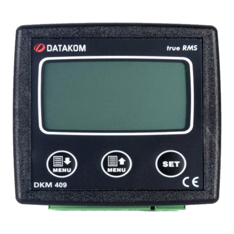
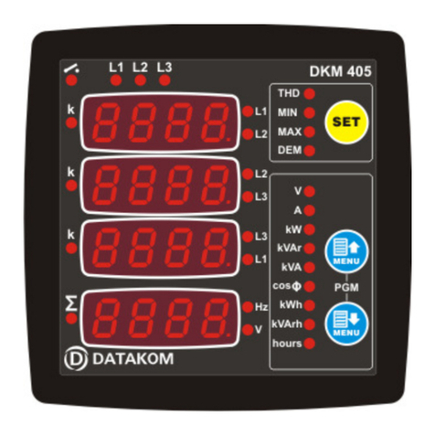
Datakom DKM-411 Instructions for use

DKM-411 Modbus Application Manual V3.0 (15.01.2017)
- 1 -
MODBUS APPLICATION MANUAL
DKM-411

DKM-411 Modbus Application Manual V3.0 (15.01.2017)
- 2 -
Any unauthorized use or copying of the contents or any part of this document is prohibited.
This applies in particular to trademarks, model denominations, part numbers and drawings.
This document describes minimum required details for the successfull interfacing of the DKM-411 family
units to 3rd party Modbus and Modbus-TCP/IP based applications.
Follow carefully advices given in the document. These are often good practices for the installation of
genset control units which reduce future issues.
For all technical queries please contact Datakom at below e-mail address:
datakom@datakom.com.tr
This document will apply to both Modbus through RS-485 and Modbus-TCP/IP communications.
FILENAME
DESCRIPTION
411_USER
DKM-411 User Manual
411-Ethernet Configuration
Ethernet Configuration Guide for DKM-411
411-GSM Configuration
GSM Configuration Guide for DKM-411
REVISION
DATE
AUTHOR
DESCRIPTION
01
14.02.2013
MH
First issue, firmware version 1.0
02
05.11.2013
MH
Added counter, min, max registers
03
12.09.2014
MH
Fix location of alarm registers
04
14.04.2015
MH
Added unique ID, network IP registers
05
11.09.2015
MH
Updated for firmware V2.2
06
15.02.2017
TO
Modbus Registers Updated
CAUTION: Potential risk of injury or death.
WARNING: Potential risk of malfunction or material damage.
ATTENTION: Useful hints for the understanding of device operation.
SCOPE OF THIS DOCUMENT
TERMINOLOGY
REVISION HISTORY
RELATED DOCUMENTS
ABOUT THIS DOCUMENT
COPYRIGHT NOTICE

DKM-411 Modbus Application Manual V3.0 (15.01.2017)
- 3 -
The Modbus communication is widely used in the connection of industrial control units to various
management systems for remote monitoring and control. It has begun the basic industry standard in the
last decades.
The unit offers the possibility of MODBUS communication through below carriers:
-RS485 serial port, with adjustable baud rate between 2400 and 115200 bauds
-MODBUS-TCP/IP through Ethernet port (10/100Mb)
-MODBUS-TCP/IP through GSM-GPRS modem. (84/42kb)
Detailed description about the MODBUS protocol is found in the document “Modicon Modbus Protocol
Reference Guide”.This document may be downloaded at: www.modbus.org/docs/PI_MBUS_300.pdf
Detailed description about the MODBUS-TCP/IP protocol is found in the document “MODBUS
APPLICATION PROTOCOL SPECIFICATION”.This document may be downloaded at:
http://www.modbus.org/docs/Modbus_Application_Protocol_V1_1b.pdf
The MODBUS properties of the unit are:
-Data transfer mode: RTU
-Serial data: selectable baud rate, 8 bit data, no parity, 1 bit stop
-Modbus-TCP/IP: Ethernet 10/100Mb or GPRS Class 10.
-Supported functions:
-Function 3 (Read multiple registers)
-Function 6 (Write single register)
-Function 16 (Write multiple registers)
Each register consists of 2 bytes (16 bits). A larger data structure will contain multiple registers.
The Modbus communications requires a slave address to be assigned to each device in the Modbus
network. This address ranges between 1 and 240 and allows the addressing of different slave devices in
the same network.
Devices using Modbus-TCP/IP with different IP or port
addresses may use any slave address. It is advised to set
these slave addresses to the default setting which is 1.
Each device in the same RS-485 serial network must be
assigned a different slave address. Otherwise the Modbus
communications will not be performed.
MODBUS CONFIGURATION
MODBUS COMMUNICATION BASICS

DKM-411 Modbus Application Manual V3.0 (15.01.2017)
- 4 -
Modbus Slave Address: may be set between 1 and 240
RS-485 Enable: must be set to 1 (or checkbox enabled)
RS-485 Baud Rate: selectable between 2400 and 115200 bauds. All devices in the same network must
use the same Baud Rate.
The complete RS-485 port specifications are found in the DKM-411 User Manual.
Selecting a higher baud rate will allow faster communication, but will reduce the communication distance.
Selecting a lower baud rate will increase the communication distance, but will cause slower response
times.
Typically 9600 bauds will allow 1200m distance with special balanced 120 ohms cable.
Modbus Slave Address: may be set between 1 and 240. If only one unit is available in the same IP
address, it is advised to keep the default address (1).
Ethernet Enable: This parameter should be set to 1 (or checked) in order to enable the ethernet port.
Modbus TCP/IP Port: The usual setting is 502. However the unit is able to work on any port address.
User IP Mask: There are 3 mask registers available. The use of the registers are emphasized in the D-
500/700 User Manual. Please set the first mask as 255.255.255.0 for the proper operation.
Ethernet Network IP: May be left as 0.0.0.0 for automatic address claim or set to a value in order to claim
a defined address.
Ethernet Gateway IP: Should be set in accordance with your local switch configuration.
Ethernet Subnet Mask: Should be set in accordance with your local switch configuration.
The complete Ethernet port specifications are found in the DKM-411 User Manual.
Please rewiev the document Ethernet Configuration Guide for DKM-411 for more details about the
ethernet port setup.
Modbus Slave Address: may be set between 1 and 240. If only one unit is available in the same IP
address, it is advised to keep the default address (1).
Modem Selection: Internal or external following your configuration.
Modem Baud Rate: Selectable only for external modem. 115200 bauds advised. Selecting a lower baud
rate will slow down communication between the controller and the modem.
GPRS Connection Enable: This parameter should be set to 1 (or checked).
Modbus TCP/IP Port: Set this value to 80.
User IP Mask: There are 3 mask registers available. The use of the registers are emphasized in the DKM-
411 User Manual. Please set the first mask as 255.255.255.0 for the proper operation.
Parameters required for Modbus-TCP/IP through GSM_GPRS Modem
Parameters required for Modbus-TCP/IP through Ethernet port
Parameters required for RS-485 Modbus operation

DKM-411 Modbus Application Manual V3.0 (15.01.2017)
- 5 -
Modbus
address
RS-485
port enable
RS-485
Baud Rate
Modbus-TCP/IP
port
Modem
Selection
Modem
Baud Rate

DKM-411 Modbus Application Manual V3.0 (15.01.2017)
- 6 -
User IP
Masks
Ethernet
port enable
Ethernet IP
address
Ethernet
gateway IP
Ethernet
subnet
mask
GPRS
enable

DKM-411 Modbus Application Manual V3.0 (15.01.2017)
- 7 -
The function 03 (read multiple registers) will be used for data reading. The MODBUS master will send a
query. The answer will be one of the below:
-A response containing the requested data
-An exceptional response indicating a read error.
The maximum number of registers read in one message is 16. If more registers are requested, the
unit will send only the first 16 registers.
The query message specifies the starting register and quantity of registers to be read. The
message structure is below:
Byte
Description
Value
0
Controller address
1 to 240
1
Function code
3
2
Starting address high
See below the description of available registers
3
Starting address low
4
Number of registers high
always 0
5
Number of registers low
max 10h (16 decimal)
6
CRC low byte
See below for the checksum calculation
7
CRC high byte
Here is the sequence to read 16 registers starting from address 20h (32 decimal):
01 03 00 20 00 10 45 CC (each byte is expressed as 2 hexadecimal characters)
The checksum value in the above message may be used for the verification of checksum
calculation algorithm.
The normal response will be:
Byte
Description
Value
0
Controller address
same as in the query
1
Function code
3
2
Data lenght in bytes (L)
number of registers * 2
3
High byte of 1st register
4
Low byte of 1st register
5
High byte of 2nd register
6
Low byte of 2nd register
....
L+1
High byte of the last register
L+2
Low byte of the last register
L+3
CRC low byte
See below for the checksum calculation
L+4
CRC high byte
The exceptional response will be:
Byte
Description
Value
0
Controller address
same as in the query
1
Function code
131 (function code + 128)
2
Exception code
2 (illegal address)
3
CRC low byte
See below for the checksum calculation
4
CRC high byte
DATA READING

DKM-411 Modbus Application Manual V3.0 (15.01.2017)
- 8 -
The function 06 (write single register) and the function 16 (write multiple registers) are used for data
writing.
The MODBUS master will send a query containing data to be written. The answer will be one of the below:
-A normal response confirming successful write,
-An exceptional response indicating a write error.
Only some of the available registers are authorized to be written. An attempt to write a write protected
register will result to the exceptional response.
The query message specifies the register address and data. The message structure is below:
Byte
Description
Value
0
Controller address
1 to 240
1
Function code
6
2
Register address high
See below the description of available registers
3
Register address low
4
Data high byte
5
Data low byte
6
CRC low byte
See below for the checksum calculation
7
CRC high byte
Here is the sequence to write the value 0010h to the register 40h (64 decimal):
01 06 00 40 00 10 89 D2 (each byte is expressed as 2 hexadecimal characters)
The checksum value in the above message may be used for the verification of checksum calculation
algorithm
The normal response will be the same as the query:
Byte
Description
Value
0
Controller address
1 to 240
1
Function code
6
2
Register address high
See below the description of available registers
3
Register address low
4
Data high byte
5
Data low byte
6
CRC low byte
See below for the checksum calculation
7
CRC high byte
The exceptional response will be:
Byte
Description
Value
0
Controller address
same as in the query
1
Function code
134 (function code + 128)
2
Exception code
2 (illegal address)
or
10 (write protection)
3
CRC low byte
See below for the checksum calculation
4
CRC high byte
DATA WRITING (SINGLE REGISTER)

DKM-411 Modbus Application Manual V3.0 (15.01.2017)
- 9 -
The function 06 (write single register) and the function 16 (write multiple registers) are used for data
writing.
The MODBUS master will send a query containing data to be written. The answer will be one of the below:
-A normal response confirming successful write,
-An exceptional response indicating a write error.
Only some of the available registers are authorized to be written. An attempt to write a write protected
register will result to the exceptional response.
The query message specifies the register address and data. The message structure is below:
Byte
Description
Value
0
Controller address
1 to 240
1
Function code
16
2
Starting address high
See below the description of available registers
3
Starting address low
4
Number of registers high
always 0
5
Number of registers low
max ??
6
Data lenght in bytes (L)
number of registers * 2
7
High byte of 1st register
8
Low byte of 1st register
9
High byte of 2nd register
10
Low byte of 2nd register
....
L+5
High byte of the last register
L+6
Low byte of the last register
L+7
CRC low byte
See below for the checksum calculation
L+8
CRC high byte
The normal response is below:
Byte
Description
Value
0
Controller address
1 to 240
1
Function code
16
2
Starting address high
See below the description of available registers
3
Starting address low
4
Number of registers high
always 0
5
Number of registers low
max ??
6
CRC low byte
See below for the checksum calculation
7
CRC high byte
The exceptional response will be:
Byte
Description
Value
0
Controller address
same as in the query
1
Function code
144 (function code + 128)
2
Exception code
2 (illegal address)
or
10 (write protection)
3
CRC low byte
See below for the checksum calculation
4
CRC high byte
DATA WRITING (MULTIPLE REGISTERS)

DKM-411 Modbus Application Manual V3.0 (15.01.2017)
- 10 -
Here is a procedure for generating a CRC:
1) Load a 16–bit register with FFFF hex (all 1’s). Call this the CRC register.
2) Exclusive OR the first 8–bit byte of the message (the function code byte) with the low–order byte of the
16–bit CRC register, putting the result in the CRC register.
3) Shift the CRC register one bit to the right (toward the LSB), zero–filling the MSB. Extract and examine
the LSB. The LSB is the least significant bit of the CRC before the shift operation.
4) If the LSB is 1: Exclusive OR the CRC register with the polynomial value A001 hex.
5) Repeat Steps 3 and 4 until 8 shifts have been performed. Thus, a complete 8–bit byte will be processed.
6) Repeat Steps 2 through 5 for the next 8–bit byte of the message. Continue doing this until all bytes have
been processed.
7) The final contents of the CRC register is the CRC value.
8) Place the CRC into the message such that the low byte is transmitted first. The algorithm should give
the correct CRC for below messages:
01 03 00 20 00 10 45 CC
01 06 00 40 00 10 89 D2
Error codes
Only 3 error codes are used:
01: illegal function code
02: illegal address
10: write protection (attempt to write a read_only register)
Data types
Each register consists of 16 bits (2 bytes)
If the data type is a byte, only the low byte will contain valid data. High byte is don’t care.
For data type longer than 16 bits, consecutive registers are used. The least significant register
comes first.
16bit variables: These variables are stored in a single register. Bit_0 denotes the LSB and bit 15 denotes
the MSB.
32 bit variables: These variables are stored in 2 consecutive registers. The high order 16 bits are in the
first register and the low order 16 bits are in the second register
Bit arrays: Arrays larger than 16 bits are stored in multiple registers. The LSB of the first register is bit_0.
The MSB of the first register is bit_15. The LSB of the second register is bit_16. The MSB of the second
register is bit_31, and so on.
DATA FORMATS
CRC CALCULATION

DKM-411 Modbus Application Manual V3.0 (15.01.2017)
- 11 -
ADDRESS
(decimal)
R / W
DATA
SIZE
COEFF.
DESCRIPTION
8192
R / W
16bit
-
Year (0-4095)
8193
R / W
16bit
-
Month (1-12)
8194
R / W
16bit
-
Date (1-31)
8195
R
16bit
-
Day of Week (0-6)
8196
R / W
16bit
-
Hours (0-23)
8197
R / W
16bit
-
Minutes (0-59)
8198
R / W
16bit
-
Seconds (0-59)
8199
R / W
16bit
-
Year (0-4095) (UTC)
8200
R / W
16bit
-
Month (1-12) (UTC)
8201
R / W
16bit
-
Date (1-31) (UTC)
8202
R
16bit
-
Day of Week (0-6) (UTC)
8203
R / W
16bit
-
Hours (0-23) (UTC)
8214
R / W
16bit
-
Minutes (0-59) (UTC)
8215
R / W
16bit
-
Seconds (0-59) (UTC)
ADDRESS
(decimal)
R / W
DATA
SIZE
COEFF.
DESCRIPTION
12288
R / W
32bit
x10
kWh_1 import
12290
R / W
32bit
x10
kWh_1 export
12292
R / W
32bit
x10
kVArh_1 inductive
12294
R / W
32bit
x10
kVArh_1 capacitive
12296
R / W
32bit
x10
Group_1 Hour Counter
12298
R / W
32bit
x10
kWh_2 import
12300
R / W
32bit
x10
kWh_2 export
12302
R / W
32bit
x10
kVArh_2 inductive
12304
R / W
32bit
x10
kVArh_2 capacitive
12306
R / W
32bit
x10
Group_2 Hour Counter
12332
R / W
32bit
x1
Digital Input 1 Counter
12334
R / W
32bit
x1
Digital Input 2 Counter
REGISTER DEFINITIONS

DKM-411 Modbus Application Manual V3.0 (15.01.2017)
- 12 -
ADDRESS
(decimal)
R / W
DATA
SIZE
COEFF.
DESCRIPTION
12460
R
32bit
x10
Demand I1
12462
R
32bit
x10
Demand I2
12464
R
32bit
x10
Demand I3
12466
R
32bit
x10
Demand In
12468
R
32bit
x100
Demand kW
12470
R
32bit
x100
Demand kVAr
12472
R
32bit
x10
Minimum V1
12474
R
32bit
x10
Minimum V2
12476
R
32bit
x10
Minimum V3
12478
R
32bit
x10
Minimum U12
12480
R
32bit
x10
Minimum U23
12482
R
32bit
x10
Minimum U31
12484
R
32bit
x10
Minimum I1
12486
R
32bit
x10
Minimum I2
12488
R
32bit
x10
Minimum I3
12490
R
32bit
x10
Minimum In
12492
R
32bit
x100
Minimum Frequency
12494
R
32bit
x100
Minimum kW import
12496
R
32bit
x100
Minimum kW export
12498
R
32bit
x100
Minimum kVAr inductive
12500
R
32bit
x100
Minimum kVAr capacitive
12502
R
32bit
x10
Maximum V1
12504
R
32bit
x10
Maximum V2
12506
R
32bit
x10
Maximum V3
12508
R
32bit
x10
Maximum U12
12510
R
32bit
x10
Maximum U23
12512
R
32bit
x10
Maximum U31
12514
R
32bit
x10
Maximum I1
12516
R
32bit
x10
Maximum I2
12518
R
32bit
x10
Maximum I3
12520
R
32bit
x10
Maximum In
12522
R
32bit
x100
Maximum Frequency
12524
R
32bit
x100
Maximum kW import
12526
R
32bit
x100
Maximum kW export
12528
R
32bit
x100
Maximum kVAr inductive
12530
R
32bit
x100
Maximum kVAr capacitive

DKM-411 Modbus Application Manual V3.0 (15.01.2017)
- 13 -
ADDRESS
(decimal)
R / W
DATA
SIZE
COEFF.
DESCRIPTION
20480
R
32bit
x10
Phase L1 voltage
20482
R
32bit
x10
Phase L2 voltage
20484
R
32bit
x10
Phase L3voltage
20486
R
32bit
x10
Phase L1-L2 voltage
20488
R
32bit
x10
Phase L2-L3 voltage
20490
R
32bit
x10
Phase L3-L1voltage
20492
R
32bit
x10
Phase L1 current
20494
R
32bit
x10
Phase L2 current
20496
R
32bit
x10
Phase L3 current
20498
R
32bit
x10
Neutral current
20500
R
32bit
x100
Phase L1 active power
20502
R
32bit
x100
Phase L2active power
20504
R
32bit
x100
Phase L3active power
20506
R
32bit
x100
Total active power
20508
R
32bit
x100
Phase L1 reactive power
20510
R
32bit
x100
Phase L2reactive power
20512
R
32bit
x100
Phase L3reactive power
20514
R
32bit
x100
Total reactive power
20516
R
32bit
x100
Phase L1 apparent power
20518
R
32bit
x100
Phase L2apparent power
20520
R
32bit
x100
Phase L3apparent power
20522
R
32bit
x100
Total apparent power
20524
R
16bit
x1000
Phase L1 power factor
20525
R
16bit
x1000
Phase L2power factor
20526
R
16bit
x1000
Phase L3power factor
20527
R
16bit
x1000
Total power factor
20528
R
16bit
x100
Frequency
20529
-
-
-
-
20530
-
-
-
-
20531
-
-
-
-
20532
R
32bit
x10
Average Ph-N voltage
20534
R
32bit
x10
Average Ph-Ph voltage
20536
R
32bit
x10
Average current
20538
R
16bit
x10
Phase L1 tangent(teta) Q1/P1
20539
R
16bit
x10
Phase L2 tangent(teta) Q2/P2
20540
R
16bit
x10
Phase L3 tangent(teta) Q3/P3
20541
R
16bit
x10
Total tangent(teta) Q/P
20542
R
16bit
x10
Voltage Unbalance %
20543
R
16bit
x10
Current Unbalance %

DKM-411 Modbus Application Manual V3.0 (15.01.2017)
- 14 -
ADDRESS
(decimal)
R / W
DATA
SIZE
COEFF.
DESCRIPTION
20548 ...
R
4624bit
289x16
-
Phase L1 voltage, harmonics and waveform buffer
20837 ...
R
4624bit
289x16
-
Phase L2 voltage, harmonics and waveform buffer
21126 ...
R
4624bit
289x16
-
Phase L3 voltage, harmonics and waveform buffer
21415 ...
R
4624bit
289x16
-
Phase L1-2 voltage, harmonics and waveform buffer
21704 ...
R
4624bit
289x16
-
Phase L2-3 voltage, harmonics and waveform buffer
21993 ...
R
4624bit
289x16
-
Phase L3-1 voltage, harmonics and waveform buffer
22282 ...
R
4624bit
289x16
-
Phase L1 current, harmonics and waveform buffer
22571 ...
R
4624bit
289x16
-
Phase L2 current, harmonics and waveform buffer
22860 ...
R
4624bit
289x16
-
Phase L3 current, harmonics and waveform buffer
BUFFER STRUCTURE
The buffer consists of 289 x 16 bit registers. The structure is below.
ADDRESS
(decimal)
R / W
DATA
SIZE
COEFF.
DESCRIPTION
BASE+0
R
16bit
x10
THD of this channel
BASE+1
R
512bit
32x16
x10
This string of 32 registers carry individual harmonics of the
selected channel, staring from H#01 until H#63. The first
register represents the fundamental and is always set to
100.0%.
BASE+33
R
4096bit
256x16
x1
Scopemeter dataof the channel. Each register represents one
point in the X axis of the scopemeter. The complete waveform
is represented with 256 horizontal points. The register value is
a signed integer.
The sampling rate is 122us. Thus the buffer length is
256x122us, namely 31ms, presenting more than 1 cycle of the
waveform.
By representing these values in graphical form, a software
oscilloscope can be made.
HARMONICS AND WAVEFORM INFORMATION

DKM-411 Modbus Application Manual V3.0 (15.01.2017)
- 15 -
ADDRESS
(decimal)
R / W
DATA
SIZE
COEFF.
DESCRIPTION
23440
R
64bit
-
Alarm bits. Bit definitions are given at the end of the document.
23444
R
64bit
-
Warning bits. Bit definitions are given at the end of the
document.
Bit_0: Input_1 warning
Bit_1: Input_2 warning
23448
R
128bit
-
Relay function bits. Each bit represent the activation status of
the related function. The list of relay function bits is given at the
end of this document.
23456
R
16bit
-
Input alarm bits.
Bit_0: Input_1 alarm
Bit_1: Input_2 alarm
23464
R
16bit
-
Phasor diagram: phase angle of voltage V2 (V1 angle = 0)
23465
R
16bit
-
Phasor diagram: phase angle of voltage V3 (V1 angle = 0)
23466
R
16bit
-
Phasor diagram: phase angle of voltage I1 (V1 angle = 0)
23467
R
16bit
-
Phasor diagram: phase angle of voltage I2 (V1 angle = 0)
23468
R
16bit
-
Phasor diagram: phase angle of voltage I3 (V1 angle = 0)
23469
R
16bit
-
Topology:
0: 3 phase, 4 wire star
1: single phase, 2 wire
2: 2 phase, 3 wire L1-L2
3: 3 phase, 3 wire
4: 3 phase, 4 wire delta
5: 3 phase, 3 wire, 2CTs L1-L2
6: 3 phase, 3 wire, 2CTs L1-L3
23475-
23480
R
12byte
-
Device Unique ID, 24 hexadecimal characters
23481
R
16bit
x100
K Factor I1
23482
R
16bit
x100
K Factor I2
23483
R
16bit
x100
K Factor I3
23484
R
16bit
x100
K Factor Ia
23492
R
16bit
-
Device ID (0411h)
23493
R
16bit
-
Device Hardware version
23494
R
16bit
-
Device Software version
23499
R
16bit
-
Successful IP packet counter
23500
R
32bit
-
GPRS IP Address
23502
R
32 bit
-
Network (LAN) IP address
23522-
23529
R
128bit
-
Modem IMEI number

DKM-411 Modbus Application Manual V3.0 (15.01.2017)
- 16 -
00: High Voltage
01: Low Voltage
02: High Frequency
03: Low Frequency
04: High kW
05: Low kW
06: High kVAr
07: Low kVAr
08: High power factor
09: Low power factor
10: High Current
11: High THD-V
12: High THD-I
13: Voltage Unbalance
14: Current Unbalance
15: Wrong Phase Sequence
16..63: Reserved Alarms
00: Horn
01: Flashing relay
02: Phase order fail
03: Voltage fail
04: Voltage ok
05: Alarm
06: -
07: Warning
08: -
09: kWh Tick
10: kVArh Tick
11: Low voltage alarm
12: High voltage alarm
13: Low frequency alarm
14: High frequency alarm
15: Frequency alarm
16: Low active power alarm
17: High active power alarm
18: Active power alarm
19: Capacitive reactive power alarm
20: Inductive reactive power alarm
21: Reactive power alarm
22: Capacitive power factor alarm
23: Inductive power factor alarm
24: Power factor alarm
25: High current alarm
26: High THD-V alarm
27: High THD-I alarm
28: High THD alarm
29: Voltage unbalance alarm
30: Current unbalance alarm
31: Unbalance alarm
32: Input 1 alarm
33: Input 2 alarm
34: -
35: -
36: -
37: -
38: -
39: -
40: Button 1
41: Button 2
42: Button 3
43: Button 4
48: Input 1
49: Input 2
50: Remote Output 1
51: Remote Output 2
52: Daylight Relay
LIST OF RELAY FUNCTION BITS
LIST OF ALARM BITS
Other manuals for DKM-411
2
Table of contents
Other Datakom Measuring Instrument manuals

Datakom
Datakom DKM-407 User manual
Datakom
Datakom DKM-411 User manual
Datakom
Datakom DKM-409-PRO-AT User manual
Datakom
Datakom DVF-0303 User manual

Datakom
Datakom DKM-430 User manual

Datakom
Datakom DPR-165 User manual
Datakom
Datakom DPR-350 Series User manual
Datakom
Datakom DSD-080 User manual

Datakom
Datakom DKM-411 User manual
Datakom
Datakom DKM-407 User manual

