Davicom DM9000A Supplement

DM9000A
APPLICATION NOTES
Preliminary 1
Version: DM9000A-AN-V121
November 27, 2007
DM9000A
16 / 8 Bit Ethernet Controller
with General Processor Interface
Application Notes V1.21
Technical Reference Manual
Davicom Semiconductor, Inc

DM9000A
APPLICATION NOTES
Preliminary 2
Version: DM9000A-AN-V121
November 27, 2007
1INTRODUCTION.................................................................................................6
1.1 General Description..................................................................................................................6
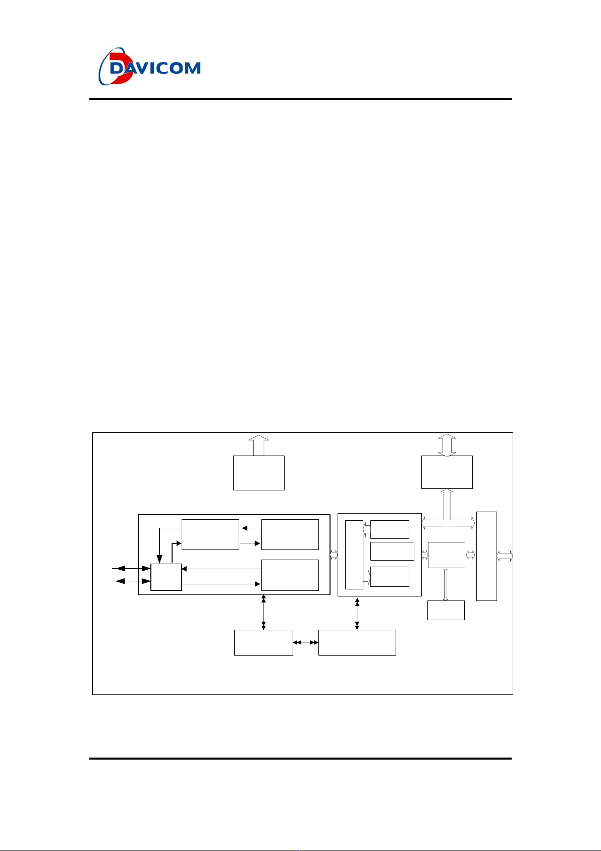
2GENERALPROCESSOR BUS DESCRIPTION...............................................7
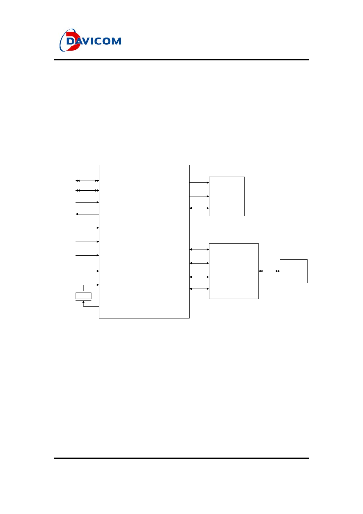
2.1 Typical Signal Connection with Processor Bus.........................................................................7
2.1.1 Pin Function Table.............................................................................................................8
2.1.2 Processor Parallel Bus 8/ 16-Bit Mode Setting..................................................................8
2.1.3 Command Type...................................................................................................................9
3SYSTEM HARDWARE DESIGN......................................................................10
3.1 How to Select Chip..................................................................................................................10
3.2 Strap Pins Setting....................................................................................................................10
3.3 Serial EEPROM Operation.....................................................................................................10
3.3.1 EEPROM Format.............................................................................................................11
3.4 GPIO Pins Setting...................................................................................................................15
3.5 Schematic Reference Design...................................................................................................17
3.5.1 Application Schematics for 8-Bit and 16-Bit....................................................................17
4RESETOPERATIONAND PHYPOWER-DOWN MODE...........................19
4.1 Power On Reset.......................................................................................................................19
4.2 Software Reset.........................................................................................................................19
4.3 PHY Power Down Mode.........................................................................................................19
4.3.1 GPR PHYPD Setting........................................................................................................20
4.3.2 PHY Register Setting........................................................................................................20
5HOWTO PROGRAM DM9000A......................................................................21
5.1 How to Read/ Write DM9000A Register .................................................................................21
5.2 Driver Initializing Steps..........................................................................................................22
5.3 How to Read/ Write EEPROM Data .......................................................................................23
5.3.1 HOWTO Read EEPROM Data ......................................................................................23
5.3.2 HOWTO Write EEPROM Data......................................................................................24
5.4 How to Read/ Write PHY Register ..........................................................................................26
5.4.1 HOWTO Read PHY Register..........................................................................................26
5.4.2 HOWTO Write PHY Register .........................................................................................27
5.5 How to Transmit Packets ........................................................................................................28

DM9000A
APPLICATION NOTES
Preliminary 3
Version: DM9000A-AN-V121
November 27, 2007
5.5.1 Packet Transmission.......................................................................................................28
5.5.2 To Check a Completion Flag..........................................................................................29
5.6 How to Receive Packets..........................................................................................................30
5.6.1 Receive Interrupt Service Routine..................................................................................30
5.6.2 Packet Reception............................................................................................................31
5.6.3 To Check the Packet Status and Length..........................................................................31
5.6.4 Receive the Packet's Data..............................................................................................32
6THE OTHERS.....................................................................................................33
6.1 How to transmit and receive more than 2048-byte packets.....................................................33
6.2 The performance of DM9000A................................................................................................33
6.3 WOL (Wake-up on LAN)..........................................................................................................33
6.4 IP/TCP/UDP checksums Offload............................................................................................37
6.5 AUTO-MDIX and Application.................................................................................................38

DM9000A
APPLICATION NOTES
Preliminary 4
Version: DM9000A-AN-V121
November 27, 2007
FIGURE 1.1 DM9000AINTERNALBLOCK DIAGRAM.................................................................6
FIGURE 2.1 SIGNALCONNECTION WITHAPROCESSOR INTERFACING ..............................7
FIGURE 2.2 CMD PINAND PROCESSOR INTERFACE.................................................................9
FIGURE 3.1 SCHEMATIC FOR 8-BITPROCESSOR .....................................................................17
FIGURE 3.2 SCHEMATIC FOR 16-BIT PROCESSOR ...................................................................18
FIGURE 5.1 PACKET TRANSMITTING BUFFER.........................................................................28
FIGURE 5.2 BLOCK DIAGRAM OF THE RECEIVED PACKETS................................................30
FIGURE 6.1AUTO-MDIX 10BASE-T/100BASE-TXAPPLICATION...........................................38

DM9000A
APPLICATION NOTES
Preliminary 5
Version: DM9000A-AN-V121
November 27, 2007
TABLE 2.1 PIN FUNCTION TABLE FOR PROCESSOR INTERFACE ...........................................8
TABLE 3.1 STRAPPIN CONTROLTABLE....................................................................................10
TABLE 3.2 EEPROM FORMAT IN 16-BITMODE .........................................................................11
TABLE 3.3 EEPROM FORMAT IN 8-BITMODE ...........................................................................13
TBALE 3.4 GENERAL PURPOSE CONTROLREGISTER (GPCR) TABLE.................................15
TABLE 3.5 GENERALPURPOSE REGISTER (GPR) TABLE .......................................................16

DM9000A
APPLICATION NOTES
Preliminary 6
Version: DM9000A-AN-V121
November 27, 2007
1 Introduction
1.1 General Description
The DM9000A is a fully integrated, powerful and cost-effective Fast Ethernet MAC controller
with a general processor interface, an EEPROM interface, a 10/100 PHY and 16K Byte
SRAM (13K Byte for RX FIFO and 3K Byte for TX FIFO). It is designed with low power,
single-voltage and high performance process that supports 3.3V with 5V tolerant I/O. Besides,
the DM9000A supports 8/ 16-bit processor interface to internal memory accesses for many
different processors. It is good integrated 10/100 Mbps transceiver with AUTO-MDIX and
IP/TCP/UDP-Checksum Offload.
The goal of this document is for the embedded design engineers, to implement the DM9000A
LAN chip on any processor's architecture quickly and successfully, with providing the exact
reference information and pertaining to many embedded systems. The software programming
is very simple, so users can port the software drivers to any system easily.
LED
TX+/-
RX+/-
Autonegotiation
RX Machine
TX Machine
MAC
MII
-
/
PHYceiver
Processer
Interface
Auto-
MDIX
EEPROM
Interface
Memory
Management
Internal
SRAM
&
MII Management
Control
MII Register
10 Base T
Tx Rx
100BaseTX
transceiver 100Base-TX
PCS
&Control Status
Registers
Figure 1.1 DM9000A Internal Block Diagram.

DM9000A
APPLICATION NOTES
Preliminary 7
Version: DM9000A-AN-V121
November 27, 2007
2 General Processor Bus Description
This chapter is intended to aid design engineers connecting the DM9000A device to a
micro-processor or micro-controller. The discussion will include the pin functional table, and
the individual control signals of the DM9000A involved in the connection between the device
and an associated micro-processor/ micro-controller in detail.
EEPROM
93C46/ LC46
AUOT-MDIX
Transformer RJ-45
25Mhz
CMD (32)
CS# (37)
A2
nCS
EECS (21)
EECK (20)
EEDIO (19)
DM9000A
TXO+ (7)
TXO- (8)
RXI+ (3)
RXI- (4)
X1 (44)
X2 (43)
IOR# (35)
IOW# (36)
INT (34)
PWRST# (40)
INT
nRD
nWR
SD0~SD7 (18~10)
SD8~SD15 (31~22)
D0~D7
D8~D15
Power
On
Reset
Figure 2.1 Signal Connection with a Processor Interfacing.
2.1 Signals Connection with Processor Bus
The DM9000A can interface directly with most general processors local bus such as ARM,
MIPS, Intel, TI, Motorola, NEC, and Hitachi... It is designed to suit for the implementation of
Fast Ethernet connectivity solutions to many embedded systems.

DM9000A
APPLICATION NOTES
Preliminary 8
Version: DM9000A-AN-V121
November 27, 2007
2.1.1 Pin Function Table
Note: The pins of processor parallel interface all have a pulled down resistor about 60K Ohm
internally.
Processor
Bus Signal DM9000A
Signal Pin No. I/O Description
nRD IOR# 35 I Processor READ Command
This pin is low active at default; its polarity can be modified by the
EEPROM setting.
nWR IOW# 36 I Processor WRITE Command
This pin is low active at default; its polarity can be changed by the
EEPROM setting.
nCS /
nAEN CS# 37 I Chip Select
A low active signal is used to select the DM9000A. Its polarity can be
changed by the EEPROM setting.
SD0 ~ 7 SD0 ~ 7 18,17,16
14,13,12
,11,10
I/O DATA Bus 0 ~ 7
SD8 ~ 15 SD8 ~ 15 31,29,28
27,26,25
,24,22
I/O DATA Bus 8 ~ 15 (in 16-bit mode)
CMD CMD 32 I Command Type
When low, the access of this command cycle is INDEX port
When high, the access of this command cycle is DATA port
INT INT 34 O Interrupt Request
This pin is high active and open-collected at default; its polarity and its
output type can be modified by the EEPROM setting.
Table 2.1 Pin Function Table for Processor Interface
2.1.2 8/ 16-Bit Mode Setting
There are two operation modes of DATA bus width, 8-bit or 16-bit, when access to the internal
memory in the DM9000A. These two modes are selected by the strap pin 21 EECS shown the
following table:
EECS (pin 21) DATAwidth
0 16-bit
1 8-bit
Where, "1" means pull-high with the 10K Ohm resistor, and "0" means floating (default).
The status of DATAwidth operation mode can be examined from Bit [7] of ISR REG. FEH,
ISR (REG. FEH) IOMODE (DATAwidth)
Bit [7] Operation
0 16-bit mode
1 8-bit mode

DM9000A
APPLICATION NOTES
Preliminary 9
Version: DM9000A-AN-V121
November 27, 2007
2.1.3 Command Type
In the DM9000A, there are only two registers, named INDEX port and DATA port, which can
be accessed directly. These two ports are distinguished by the CMD pin in the access
command cycle. When CMD is low in command cycle, INDEX port is accessed; otherwise,
when CMD is high, DATAport is accessed.
All of these control and status registers in the DM9000A are accessed indirectly by the
INDEX/ DATA ports. The command sequence to access the specified control/ status register
is: firstly, to write the register’s address into INDEX port, then read/ write their data through
DATA port. The following diagram (Figure 2.2) is an example for the DM9000A CMD pin
connected to an embedded system.
The DM9000A device INDEX port
= nCS address + 0x0
The DM9000A device DATA port
= nCS address + 0x4
DM9000AProcessor
SA2
nCS
CMD
CS
Figure 2.2 CMD Pin and Processor Interface.

DM9000A
APPLICATION NOTES
Preliminary 10
Version: DM9000A-AN-V121
November 27, 2007
3 System Hardware Design
3.1 How to Select Chip
In the command cycle, the DM9000A is accessed by CS pin cooperated with IOR or IOW pins.
These pins are low active at default, while their polarity can be modified by EEPROM setting
to suit for the application of various processor types.
Both of CS pin and IOW/ IOR pin should be active to write/ read the value into INDEX port or
DATAport. So, if the IOW and IOR signals in the system are only used by the DM9000A, the
CS pin can be forced to the active logic level to simplify the system design.
3.2 Strap Pins Setting
The DM9000Aprovides the following strap pins:
Strap pins control list:
Pin Name Strap Description
20 EECK INT Polarity Type 0: INT active High
1: INT active Low
21 EECS DATA Bus Width 0: DATA 16-bit mode
1: DATA 8-bit mode
25 GP6 INT Output Type available in 8-bit modeonly
0: INT Force-Output mode
1: INT Open-Drain mode
Table 3.1 Strap Pin Control Table
Note: "1" means pull-high with the 10K Ohm resistor, and "0" means floating (default).

DM9000A
APPLICATION NOTES
Preliminary 11
Version: DM9000A-AN-V121
November 27, 2007
3.3 Serial EEPROM Operation
The DM9000A supports a serial EEPROM interface. The EEPROM of the DM9000A holds the
following parameters:
1. Ethernet node address.
2. Vendor ID and Product ID auto load.
3. Processor control bus pins polarity setting.
4. Wake-up mode control.
5. PHY ON or PHY OFF while powered up.
6. AUTO-MDIX enable/ disable setting.
7. LED1 & LED2 pins act as IO16 pin and IOWAIT/ WAKE pin in 16-bit mode.
8. LED mode 0 or mode 1 setting.
All of the above mentioned settings are read from the EEPROM upon hardware power-on
reset. The specific target device is IC 93C46, the 1024-bit serial EEPROM. (EEPROM is
93C46/ LC46 such as ATmel, Micro-chip,ATC, and CSI.)
All of accesses to the EEPROM are done in words. All of the EEPROM addresses in the
specification are specified as word addresses.
The default settings of the DM9000A can be changed by the I/O strap pins, or the EEPROM
bits settings with higher priority. The priority for setting the pins polarity is EEPROM > strap
pins > default setting.
3.3.1 EEPROM Format
Name Address
(Word) Programming
Value (Hex) Description
Ethernet
Node
Address
0 ~ 2 XX
XX
XX
XX
XX
XX
6-byte Ethernet node address.
Auto Load
Control 3 5445 Bit [1:0] = 00: Disable vendor ID and product ID programming.
*01: Accept vendor ID and product ID programming.
Bit [3:2] = 00: Disable setting of Word 6 Bit [8:0].
*01: Accept setting of Word6 Bit [8:0].
Bit [5:4]: Reserved = 0.

DM9000A
APPLICATION NOTES
Preliminary 12
Version: DM9000A-AN-V121
November 27, 2007
Bit [7:6] = 00: Disable setting of Word 7 Bit [3:0].
*01: Accept setting of Word7 Bit [3:0].
Bit [9:8]: Reserved = 0.
Bit [11:10] = 00: Disable setting of Word 7 Bit [7].
*01: Accept setting of Word 7 Bit[7].
Bit [13:12] = 00: Disable setting of Word 7 Bit [8].
*01: Accept setting of Word 7 Bit[8].
Bit [15:14] = 00: Disable setting of Word 7 Bit [15:12].
*01: Accept setting of Word 7 Bit [15:12].
Note: The remark * is now programming value.
Vendor ID 4 0A46 2-byte vendor ID.
Product ID 5 9000 2-byte product ID.
Pin Control 6 01E7 When Word 3 Bit [3:2] = 01, these bits can control the CS, IOR, IOW ,
INT, IOWAIT and IO16 pins polarity:
Bit [0] = 0: Processor CSpin is active high.
*1: Processor CS pin is active low.
Bit [1] = 0: Processor IORpin is active high.
*1: Processor IOR pin is active low.
Bit [2] = 0: Processor IOWpin is active high.
*1: Processor IOW pin is active low.
Bit [3] = *0: Processor INT pin is active high.
1: Processor INT pin is active low.
Bit [4] = *0: Processor INT pinis force output.
1: Processor INT pin is force open-collected.
Bit [5] = 0: Processor IOWAIT is active high.
*1: Processor IOWAIT is active low.
Bit [6] = 0: Processor IOWAIT is force output.
*1: Processor IOWAIT is force open-collected.
Bit [7] = 0: Processor IO16is active high.
*1: Processor IO16 is active low.
Bit [8] = 0: Processor IO16is force output.
*1: Processor IO16 is force open-collected.
Bit [15:9]: Reserved = 0.
Wake-up
Mode
Control
7 4180 Depend on the setting of Word 3 Bit [15:6] to accept auto load control:
Bit [0] = *0: WAKE pin is active high.
1:WAKEpinisactivelow.
Bit [1] = *0: WAKE pin is in level mode.
1: WAKE pin is in pulse mode.
Bit [2] = *0: Magic packet wake-up event is disabled.
1: Magic packet wake-up event is enabled.
Bit [3] = *0: Link_change wake-up event is disabled.
1: Link_change wake-up event is enabled.
Bit [6:4]: Reserved = 0.
Bit [7] = 0: LED mode 0.
*1:LEDmode1.
Bit [8] = 0: The internal PHY is disabled after power-on.
*1: The internal PHY is enabled after power-on.
The GPR REG. 1FH Bit [0] is modified from this Bit [8].
Bit [13:9]: Reserved = 0.
Bit [14] = 0: AUTO-MDIX OFF, *1: AUTO-MDIX ON.
Bit [15]: Reserved = 0.

DM9000A
APPLICATION NOTES
Preliminary 13
Version: DM9000A-AN-V121
November 27, 2007
Note: The programming value of the EEPROM is only for reference to list 16-bit values,
"XX:XX:XX:XX:XX:XX, 5445, 0A46, 9000, 01E7, 4180".
Table 3.2 EEPROM Format in 8-bit mode
Name Address
(Word) Programming
Value (Hex) Description
Ethernet
Node
Address
0 ~ 2 XX
XX
XX
XX
XX
XX
6-byte Ethernet node address.
Auto Load
Control 3 5405 Bit [1:0] = 00: Disable vendor ID and product ID programming.
*01: Accept vendor ID and product ID programming.
Bit [3:2] = 00: Disable setting of Word 6 Bit [8:0].
*01: Accept setting of Word6 Bit [8:0].
Bit [5:4]: Reserved = 0.
Bit [7:6] = 00: Disable setting of Word 7 Bit [3:0].
*01: Accept setting of Word 7 Bit [3:0] andWord 7 Bit [13:12]
= 10 to let LED2 act as WAKE in 16-bit mode only.
Bit [9:8]: Reserved = 0.
Bit [11:10] = 00: Disable setting of Word 7 Bit [7].
*01: Accept setting of Word 7 Bit[7].
Bit [13:12] = 00: Disable setting of Word 7 Bit [8].
*01: Accept setting of Word 7 Bit[8].
Bit [15:14] = 00: Disable setting of Word 7 Bit [15:12].
*01: Accept setting of Word 7 Bit [15:12].
Note: The remark * is now programming value.
Vendor ID 4 0A46 2-byte vendor ID.
Product ID 5 9000 2-byte product ID.
Pin Control 6 01E7 When Word 3 Bit [3:2] = 01, these bits can control the CS, IOR, IOW ,
INT, IOWAIT and IO16 pins polarity:
Bit [0] = 0: Processor CSpin is active high.
*1:ProcessorCSpinisactivelow.
Bit [1] = 0: Processor IORpin is active high.
*1: Processor IOR pin is active low.
Bit [2] = 0: Processor IOWpin is active high.
*1: Processor IOW pin is active low.
Bit [3] = *0: Processor INT pin is active high.
1: Processor INT pin is active low.
Bit [4] = *0: Processor INT pinis force output.
1: Processor INT pin is force open-collected.
Bit [5] = 0: Processor IOWAIT is active high.
*1: Processor IOWAIT is active low.
Bit [6] = 0: Processor IOWAIT is force output.

DM9000A
APPLICATION NOTES
Preliminary 14
Version: DM9000A-AN-V121
November 27, 2007
*1: Processor IOWAIT is force open-collected.
Bit [7] = 0: Processor IO16is active high.
*1: Processor IO16 is active low.
Bit [8] = 0: Processor IO16is force output.
*1: Processor IO16 is force open-collected.
Bit [15:9]: Reserved = 0.
Wake-up
Mode
Control
7 4180 Depend on the setting of Word 3 Bit[15:6] to accept auto load control:
Bit [0] = *0: WAKE pin is active high.
1:WAKEpinisactivelow.
Bit [1] = *0: WAKE pin is in level mode.
1: WAKE pin is in pulse mode.
Bit [2] = *0: Magic packet wake-up event is disabled.
1: Magic packet wake-up event is enabled.
Bit [3] = *0: Link_change wake-up event is disabled.
1: Link_change wake-up event is enabled.
Bit [6:4]: Reserved = 0.
Bit [7] = 0: LED mode 0.
*1:LEDmode1.
Bit [8] = 0: The internal PHY is disabled after power-on.
*1: The internal PHY is enabled after power-on.
The GPR REG. 1FH Bit [0] is modified from this Bit [8].
Bit [11:9]: Reserved = 0.
Bit [13:12] = *00: LED2 act normal.
01: LED2 act as IOWAIT in 16-bit mode only.
10: LED2 act as WAKE in 16-bit mode only.
Bit [14] = 0: AUTO-MDIX OFF,
*1:AUTO-MDIXON.
Bit [15] = *0: LED1 act normal,
1: LED1 act as IO16 in 16-bit mode only.
Note: List the programming values of the EEPROM in 16-bit mode,
"XX:XX:XX:XX:XX:XX, 5405, 0A46, 9000, 01E7, C180" if LED1 pin 39 act as "IO16".
"XX:XX:XX:XX:XX:XX, 5405, 0A46, 9000, 01E7, 5180" if LED2 pin 38 act as "IOWAIT".
"XX:XX:XX:XX:XX:XX, 5445, 0A46, 9000, 01E7, 6180" if LED2 pin 38 act as "WAKE".
"XX:XX:XX:XX:XX:XX, 5405, 0A46, 9000, 01E7, D180" if LED1 pin 39 act as "IO16" and
LED2 pin 38 act as "IOWAIT" pin used.
"XX:XX:XX:XX:XX:XX, 5445, 0A46, 9000, 01E7, E180" if LED1 pin 39 act as "IO16" and
LED2 pin 38 act as "WAKE" pin used.
Table 3.3 EEPROM Format in 16-bit mode

DM9000A
APPLICATION NOTES
Preliminary 15
Version: DM9000A-AN-V121
November 27, 2007
3.4 GPIO Pins Setting
If the DM9000A operated in 8-bit mode, there are 6 general purpose pins, GP1~GP6, can be
used. Their I/O types are controlled by GPCR REG. 1EH. And their I/O data are presented by
GPR REG. 1FH.
The default values of GPCR Bit [3:1] are all "0"s for the GP3 ~ GP1 pins as the input mode
respectively. But, the GPCR Bit [6:4] GPC64 are all forced to "1"s only for the GP6 ~ GP4
pins as the output mode.
GPCR (REG. 1EH) GPIO interface control:
Bit Name Default Description
7 RESERVED 0, RO Reserved.
6:4 GPC64 111, RO Forced to "1"s only as the output ports of GP6 ~ 4
pin 25, 26, 27.
3:1 GPC31 000, RW GP3~1 pin 28, 29, 31 set to be the input/ output port:
"1": the output port represented
"0": the input port represented.
0 RESERVED 1, RO Reserved.
Table 3.4 General Purpose Control Register (GPCR) Table
GPR (REG. 1FH) GPIO interface control:
Bit Name Default Description
7 RESERVED 0, RO Reserved.
6:4 GPO64 000, RW GP6~4 pin 25, 26, 27 are forced to the output ports
only. Set to "1": the pin output high, set to "0": the pin
output low.

DM9000A
APPLICATION NOTES
Preliminary 16
Version: DM9000A-AN-V121
November 27, 2007
3 GPIO3 0, RW
If GP3 is output port, GPR Bit [3] sets to "1" to
enable the pin 28 output high or sets to "0" to enable
the pin 28 output low.
If GP3 is input port, the value of GPR Bit [3] is "1" to
represent a high signal is received. In contract, the
value of GPR Bit [3] is "0" to represent a low signal
is received.
2 GPIO2 0, RW
If GP2 is output port, GPR Bit [2] sets to "1" to
enable the pin 29 output high or sets to "0" to enable
the pin 29 output low.
If GP2 is input port, the value of GPR Bit [2] is "1" to
represent a high signal is received. In contract, the
value of GPR Bit [2] is "0" to represent a low signal
is received.
1 GPIO1 0, RW
If GP1 is output port, GPR Bit [1] sets to "1" to
enable the pin 31 output high or sets to "0" to enable
the pin 31 output low.
If GP1 is input port, the value of GPR Bit [1] is "1" to
represent a high signal is received. In contract, the
value of GPR Bit [1] is "0" to represent a low signal
is received.
0 PHYPD 1, RW "1": power down the internal PHY
"0": power up the internal PHY.
Table 3.5 General Purpose Register (GPR) Table

DM9000A
APPLICATION NOTES
Preliminary 17
Version: DM9000A-AN-V121
November 27, 2007
3.5 Schematic Reference Design
3.5.1 Application Schematics for 8-Bit and 16-Bit
Figure 3.1 Schematic for 8-Bit Processor.
DM9000A-8/16bit TX AUTO-MIDX
2.0
DAVICOM Semiconductor Inc.
Custom
11Thursday, April 20, 2006
Title
Size Document Number Rev
Date: Sheet of
AGND
DGND
AVDD_25
DGND
AVDD_25
DVDD_33
AGND
AGND
DVDD_33
AGND
DGND
AGND
DGND
AGND
AGND
3.3V DVDD_33
DGND
CHASIS_GROUND
DGND
DGND
3.3V
CHASIS_GROUND
DVDD_33
DGND
DGND
P_IN_5V
DVDD_33
DGND
DVDD_33
DVDD_33
DVDD_33
DGND
DVDD_33 DVDD_33
DGND
DGND AGND
AGND
DGND
DGND
P_IN_5V
DGND
DGND
DGNDDGND DGNDDGND
TX-
SD12
IOR#
SD11
TX+
SD8
RX-
CMD
SD9
SD13
RX+INT
SD10
IOW#
SD1
SD9
SD13
SD4
SD2
SD6
SD5
SD10
SD8
SD12
SD0
SD15
SD7
SD11
SD14
SD3
SD1
SD9
SD13
SD4
SD2
SD6
SD5
SD10
SD8
SD12
SD0
SD15
SD7
SD11
SD14
SD3
SD1
SD9
SD13
SD4
SD2
SD6
SD5
SD10
SD8
SD12
SD0
SD15
SD7
SD11
SD14
SD3
SD1
GP2
GP6
SD4
SD2
SD6
SD5
GP3
GP1
GP5
SD0
WAKE
SD7
GP4
LED3
SD3
LED2
IOWAIT
RX-
TX-
LED1
TX+
TX- RX-
SPEED_LED
IO16
RJ_45_1
TX+
LED1
LINK_LED
RJ_45_6
RJ_45_2 RJ_45_2
RJ_45_6
RJ_45_3
RX+
RJ_45_2
LED2
RJ_45_3
LED2
RX+
LED1
RJ_45_3
RJ_45_6
RJ_45_1
SPEED_LED
RJ_45_1
LINK_LED
CS#
SD9
SD14
SD5
SD10
SD15
IOWAIT
IOW#
SD11
SD6
SD14
SD5
SD7
SD15
IO16
SD8
IOR#
SD6
CMD
CS#
SD4
SD7
SD4
INT
RST#
SD12
SD13
CS#
IOR#
IOW#
RST#
SD0
SD1
SD0
SD3
SD1
SD2
SD2
SD3
SDBUS_15
SDBUS_14
SDBUS_7
SDBUS_6
SDBUS_5
SDBUS_4
SDBUS_2
SDBUS_1
SDBUS_0
SDBUS_12 SDBUS_5
SDBUS_1
SDBUS_3
SDBUS_14
SDBUS_4
SDBUS_13
SDBUS_15
SDBUS_0
SDBUS_7
SDBUS_6
SDBUS_3
SDBUS_2
SDBUS_9
SDBUS_10
SDBUS_8
SDBUS_11
SDBUS_9
SDBUS_10
SDBUS_8
SDBUS_11
SDBUS_13
SDBUS_12
P_IN
C?
1UF
C0603
C?
1UF
C0603
U6A
Common Mode Choke
3
1 2
4
GND
P_IN P_IN
GND
C?
15PF
C0603
C?
1UF
C0603
L2
F.B/120/S0603
R14
0
R1006
D2
1N4148
SMD
A C
C?
15PF
C0603
C22
0.1UF
C0805
C21
0.1UF
C0805
C24
0.1UF
C0805
C23
0.1UF
C0805
L1
F.B/120/S0603
C4
60pF
C0603
JP3
CON3
1
2
3
C6
60pF
C0603
C5
60pF
C0603
D1
1N4148
SMD
A C
C17
0.1UF
C0603
C16
0.1UF
C0603
C7
0.1UF
C0603
R4
510
R0603
R2
510
R0603
R13
4.7K
R0603
R12
6.8K1%
R0603
C19
0.1UF
C0603
C18
0.1UF
C0603
Y1
25MHZ/49US
XTAL
C14
22PF
C0603
C?
15PF
C0603
+
C20
10UF/16V
EC-MR05-2
DM9000A-8/16bit
U2
DM9000AE/LQFP48
1
2
3
4
5
6
7
8
9
10
11
12
13
14
15
16
17
18
19
20
21
22
23
24
25
26
27
28
29
30
31
32
33
34
35
36
37
38
39
40
41
42
43
44
45
46
47
48
BGRES
AVDD25
RX+
RX-
RXGND
TXGND
TX+
TX-
AVDD25
SD7
SD6
SD5
SD4
SD3
GND
SD2
SD1
SD0
EEDIO
EEDCK
EEDCS
SD15
VDD
SD14
SD13
SD12
SD11
SD10
SD9
VDD
SD8
CMD
GND
INT
IOR#
IOW#
CS#
LED2(IOWAIT / WAKEUP for eeprom)
LED1(IO16 for eeprom)
PWRST#
TEST
VDD
X2
X1
GND
SD
RXGND
BGGND
+
C8
220UF/16V
EC-MR05-2
C?
15PF
C0603
+
C2
330UF/16V
EC-MR05-2
R?
500
R0603
R3
10K
R0603
JP4
CON3
1
2
3
C1
0.1UF
C0603
LED1 12
LED2 12
JP7
CON8
1
2
3
4
5
6
7
8
RP3
33
1
3
5
7 8
6
4
2
Q1 REGULATOR
SOT-223
I O
G
4
VIN VOUT
GND
VOUT
RP1
33
1
3
5
7 8
6
4
2
C?
15PF
C0603
C?
15PF
C0603
C?
15PF
C0603
C10
0.1UF
C0603
C11
0.1UF
C0603
R8
49.9/1%
R0603
C13
0.01UF/2KV
C12
0.1UF
C0603
R6
49.9/1%
R0603
C?
1UF
C0603
C3
0.1UF
C0603
C9
0.1UF
C0603
R7
49.9/1%
R0603
R9
75R
R0603
U3
PH163539
1
3
5
6
8 9
11
12
14
16
2
710
15
134
TD-/RD-
TD+/RD+
CT
RD-/TD-
RD+/TD+ RX+/TX+
RX-/TX-
NC
TX+/RX+
TX-/RX-
NC
NC NC
NC
MCTNC
R5
49.9/1%
R0603
R10
75R
R0603
JP6
RJ-45
1
2
3
4
5
6
7
8
R11
75R
R0603
R?
47K
R0603
JP1 JUMPER
1 2
C15
22PF
C0603
JP2 JUMPER
1 2
RP4
33
1
3
5
7 8
6
4
2
U1
93LC46/DIP8
1
2
3
4 5
6
7
8
CS
SK
DI
DO GND
NC
NC
VCC
RP2
33
1
3
5
7 8
6
4
2
JP5 HEADER/16X2
12 34 56 78 910 1112 1314 1516 1718 1920 2122 2324 2526 2728 2930 3132
R1 10K
R0603
Preliminary (for Reference Only)
8 Bit Mode16 Bit Mode
DATA BUS CONNECTOR
LINK/ACT
SPEED
JP1 ON : USE 8 Bit MODE
OFF : USE 16 Bit MODE
JP2 ON : USE EEPROM
OFF : NOT USE EEPROM
RST# LOW ACTIVE (POWER RESET)
CS# LOW ACTIVE (CHIP SELECT)
IOR# LOW ACTIVE (IO DATA READ)
IOW# LOW ACTIVE (IO DATA WRITE)
INT HIGH ACTIVE (INTERRUPT ACTIVE)
C4 , C5 , C6 NOISE FILTER
Note:
Filter IOR# , IOW# , CS# Noise
max use 60pF
[ Default OPEN ]
FOR NORMAL SYSTEM
JP3 2-3 SHORT , JP4 2-3 SHORT
FOR X86 ISA SYSTEM 16 Bit MODE TEST
JP3 1-2 SHORT , JP4 2-3 SHORT
FOR MDC/MDIO 16 Bit MODE TEST
JP3 OPEN , JP4 OPEN
CHASIS_GROUND
For EMI Solution
For EMI Solution
For EMI Solution
For EMI Solution
For EMI Solution

DM9000A
APPLICATION NOTES
Preliminary 18
Version: DM9000A-AN-V121
November 27, 2007
Figure 3.2 Schematic for 16-Bit Processor.
DM9000A 16bitdemo board
1.0
DAVICOM Semiconductor Inc.
C
11Wednesday, April 20, 2005
Title
Size Document Number Rev
Date: Sheet of
GND
GND
DVDD
AVDD_25
AGND
AGND
GND
DVDD
AGND
DVDD
GND
DVDD
DGND
VCC3
AGND
AGND
AGND
AVDD_25
AGND
DVDDVCC3
GND
DVDDDVDD_3
DVDD_5
AGNDDGND
GND
GND
VCC1.8
GND
DVDD
GND
DVDD_3
DVDD_3
GND
DVDD_3
GNDGND
DVDD
VCC1.8
DVDD
AGND
VCC1.8
VCC1.8
GND
DVDD_3
DVDD
GND
GND
GND
EECS
EECK
IOR#
SD13
RX-
TX-
INT
SD14
LED1
RX+
TX+
IOW#
CMD
SD12
SD11
SD10
SD9
SD8
SD1
LED2
RX+
RX-
LED2
LED1
EEDIO EEDIO
EECK
EECS
SD6
SD5
SD15
SD6
SD10
SD4
SD13
IOW#
SD4
CS
SD0
SD8
SD9
IOR#
SD14
INT
SD11
SD12
SD7
SD2
CMD
SD3
CS
SD15
SD0
SD2
SD1
SD3
SD7
SD5
U?
ADG3308
2
1
3
4
5
6
7
8
9
10 1111
12
13
14
15
16
17
18
19
20
A1
VCCA
A2
A3
A4
A5
A6
A7
A8
EN GNDGND
Y8
Y7
Y6
Y5
Y4
Y3
Y2
Y1
VCCY
U?
ADG3308
2
1
3
4
5
6
7
8
9
10 1111
12
13
14
15
16
17
18
19
20
A1
VCCA
A2
A3
A4
A5
A6
A7
A8
EN GNDGND
Y8
Y7
Y6
Y5
Y4
Y3
Y2
Y1
VCCY
R6
6.8K1%
R0603
R9
4.7K
R0603
R11
0R
R0603
+
C10
220UF/16V
CE5MM
C12
22PF
C0603
C13
22PF
C0603
Y1
25MHZ/49US
XTAL
DM9000A
16-bit
U2
DM9000AE/LQFP48
48
47
46
45
44
43
42
41
40
39
38
37
36
35
34
33
32
31
30
29
28
27
26
25
24
23
22
21
20
19
18
17
16
15
14
13
12
11
10
9
8
7
6
5
4
3
2
1
BGGND
RXGND
SD
GND
X1
X2
VDD
TEST
PWRST#
LED1
LED2
CS
IOW#
IOR#
INT
GND
CMD
SD8
VDD
SD9
SD10
SD11
SD12
SD13
SD14
VDD
SD15
EECS
EECK
EEDIO
SD0
SD1
SD2
GND
SD3
SD4
SD5
SD6
SD7
VDD25
TX-
TX+
TXGND
RXGND
RX-
RX+
VDD25
BGRES
C17
0.1UF
C0603
R1
10K
R0603
C18
0.1UF
C0603
+
C6
330UF/16V
CE5MM
C9
0.1UF
C19
0.01UF/2KV
C0603
C8
0.1UF
R13
49.9/1%
R0603
+
C7
220UF/16V
CE5MM
C16
0.1UF
C0603
U1
93LC46/PDIP
1
2
3
4 5
6
7
8
CS
SK
DI
DO GND
NC
NC
VCC
R8
49.9/1%
R0603
C1
0.1UF
R12
49.9/1%
R0603
C22
0.1UF
C0603
JP3
RJ-45
RJ8-45
1
2
3
4
5
6
7
8
C23
0.1UF
C0603
C15
0.1UF
C0603
C21
0.1UF
C0603
C11
0.1UF
C0603
+
C14
10UF/16V
CE5MM
C20
0.1UF
C0603
R14
75R
R0603
R15
75R
R0603
R7
49.9/1%
R0603 U4
PH163539
1
3
5
6
8 9
11
12
14
16
2
710
15
134
TD+/RD+
TD-/RD-
CT
RD+/TD+
RD-/TD- RX-/TX-
RX+/TX+
NC
TX-/RX-
TX+/RX+
NC
NC NC
NC
MCTNC
R16
75R
R0603
+
C2
100UF/16V
CE5MM C5
0.1UF
C0603
C4
0.1UF
C0603
+
C3
100UF/16V
CE5MM
Q1
LT1117-SOT223
3 2
1
IO
C
C?
0.1UF
C0603
C?
0.1UF
C0603
LED1 12 R2
510
R0603
U?
ADG3308
2
1
3
4
5
6
7
8
9
10 1111
12
13
14
15
16
17
18
19
20
A1
VCCA
A2
A3
A4
A5
A6
A7
A8
EN GNDGND
Y8
Y7
Y6
Y5
Y4
Y3
Y2
Y1
VCCY
R3
510
R0603
LED2 12
SD7
SD0
SD1
SD2
SD3
SD4
SD5
SD6
IOR#
IOW#
SD14
SD13
LED1
CMD
INT
TX-
TX+
RX-
RX+
SD8
SD9
SD10
SD11
SD12
TX-
TX+
SD15
LED2
LINK/ACT
SPEED
JP
Name
This jumper is setting chip select to EEPROM and
is also used as a strap pin to to define the LED
mode is mode 1; otherwise it is mode 0.
JP 4
JP 5
JP 6
Pulled high, the INT pin is low active;
otherwise the INT pin is high active
Select speed LED(Pin 1 and 2) and IO16(Pin 2
and 3) function for EEPROM setting
Select IOWAIT(Pin 1 and 2) and LINK/ACT
LED(Pin 2 and 3) function for EEPROM setting
JP 7
Description

DM9000A
APPLICATION NOTES
Preliminary 19
Version: DM9000A-AN-V121
November 27, 2007
4 Reset Operation and PHY Power-down Mode
The DM9000A can be reset by either hardware reset or software reset. A hardware reset can
be accomplished by the power-on reset PWRST# pin 40. A software reset can be
accomplished by setting the network control register (NCR REG. 00) RST Bit [0] = 1.
The internal PHY of the DM9000A can be powered down by writing "1" to PHYPD (the Bit [0]
of the GPR register), or by setting the Power-down Bit [11] = 1 in the PHY basic mode control
register (BMCR PHY REG. 00). In the power-down state, the power consumption is reduced
to a minimum under 21mA/ 3.3V.
4.1 Power On Reset
An active low signal is used to reset the DM9000ALAN chip. The PWRST# pin 40 is asserted
low for at least 20 ms. All of the MAC and PHY registers will be reset to the default values and
the hardware strap pins will also be latched. The DM9000A is ready after 5 us when this pin is
de-asserted and then the data will be downloaded from the EEPROM.
4.2 Software Reset
A software reset can be accomplished by setting RST Bit [0] = 1 in the network control register,
NCR REG. 00. After the reset, some registers will be reset to their default value. And the
DM9000A needs only 10 us for a software reset.
4.3 PHY Power Down Mode
In the power-down (power-saving) mode, the DM9000A will disable all the TX&RX functions.
And, it’s almost the same as the PHY SLEEP mode powered down all circuit, except oscillator
and clock generator circuit. But, it’s different to the Power Reduced mode which the TX circuit
still sends out fast link pulse with min. power consumption and wakes up if a valid signal is
detected, automatically.

DM9000A
APPLICATION NOTES
Preliminary 20
Version: DM9000A-AN-V121
November 27, 2007
There are two ways to set the power-up/ power-down mode for the internal PHY:
4.3.1 GPR PHYPD Setting
In the MAC registers, the PHYPD bit is used for powering down the internal PHY, and it is
default high "1". If the internal PHY is desired to be activated, the system driver needs to clear
this power-down bit by writing low "0" to PHYPD in the GPR REG. 1FH.
4.3.2 PHY Register Setting
In the PHY registers, the Bit [11] Power-down of the basic mode control register (BMCR REG.
00) can be set high "1" to enable the PHY power-down mode.
Table of contents
Other Davicom Controllers manuals
Popular Controllers manuals by other brands

ENGGA
ENGGA EVC800i Installation & Adjustment Manual

American Megatrends
American Megatrends MegaRAC MG9070 datasheet

Bogen
Bogen NYQUIST NQ-SYSCTRL Installation and use

Electro-Voice
Electro-Voice PWS-4 Technical specifications

Sistemes Electronics Progres
Sistemes Electronics Progres Agronic 2500 Installation

REXROTH
REXROTH CS 550i Calibration manual

ITOH DENKI
ITOH DENKI POWER MOLLER HBM-604BN Technical document

LINK-MI
LINK-MI LM-MSW1 user manual

SOMFY
SOMFY Axovia multi installation instructions

nvent
nvent raychem tcontrol-cont-03 OPERATING AND INSTALLATION Manual

Mitsubishi Electric
Mitsubishi Electric Q172CPU Programming manual

Emerson
Emerson Dixell XR75CX Series Installation and operation manual