Denon DRA-395 User manual

Hi-Fi AM-FM Stereo Receiver
SERVICE MANUAL
MODEL
DRA-395
AM-FM STEREO RECEIVER
SAFETY PRECAUTIONS ............................................ 2
SPECIFICATIONS ....................................................... 2
DISASSEMBLY ........................................................... 3
ADJUSTMENT .......................................................... 4,5
BLOCK DIAGRAM ....................................................... 6
LEVEL DIAGRAM ........................................................ 7
SEMICONDUCTORS ............................................ 8~12
PRINTED WIRING BOARDS .............................. 13~17
NOTE FOR PARTS LIST ........................................... 18
PARTS LIST OF P.W.B. UNIT ASS'Y ................. 19~24
EXPLODED VIEW ..................................................... 25
PARTS LIST OF EXPLODED VIEW ......................... 26
PACKING VIEW ........................................................ 27
— TABLE OF CONTENTS —
Some illustrations using in this service manual are slightly different from the actual set.
PARTS LIST OF PACKING & ACCESSORIES ........ 27
WIRING DIAGRAM .................................................... 28
SCHEMATIC DIAGRAMS ................................... 29~34
(1/6) INPUT UNIT ........................................................... 29
(2/6) VOLUME UNIT ....................................................... 30
(3/6) MAIN UNIT ............................................................. 31
(4/6) VIDEO UNIT ........................................................... 32
CONNECTOR UNIT ............................................... 32
(5/6) FRONT UNIT .......................................................... 33
SWITCH UNIT ........................................................ 33
POWER SW/HP UNIT ............................................ 33
(6/6) TUNER UNIT .......................................................... 34
For U.S.A. & Canada model
14-14, AKASAKA 4-CHOME, MINATO-KU, TOKYO 107-8011 JAPAN
Telephone: 03 (3584) 8111
X0118 842 NC 0108

2
DRA-395
SPECIFICATIONS
Audio Section
(Power Amplifier)
Rated output: 80W + 80W (8Ω/ohms, 20Hz ~ 20kHz with 0.08% T.H.D.)
Output terminals: A or B 4 to 16Ω/ohms
A + B 8 to 16Ω/ohms
(Analog)
LINE input - PRE OUT
Input sensitivity/input impedance: 200mV/47kΩ/kohms
Frequency response: 10Hz ~ 50kHz: ±1.5dB
S/N ratio: 100 dB (IHF-A weighted)
Total harmonic distortion: 0.009% (−3dB at rated output, 8Ω/ohms) (1kHz)
Rated output: 1.2V
PHONO input - REC OUT
Input sensitivity/input impedance: 2.5mV/47kΩ/kohms
RIAA deviation: ±0.5dB (20Hz ~ 20kHz)
S/N ratio: 74dB (IHF-A weighted, with 5mV input)
Total harmonic distortion: 0.03% (1kHz, 3V)
Rated output/Maximum output: 150mV/7V
Video Section
(Standard Video Jacks)
Input/output level and impedance: 1V p-p, 75Ω/ohms
Frequency response: 5Hz ~ 10MHz +1, −3dB
Tuner Section
[FM] (note: µV at 75Ω/ohms, 0dBf = 1×10-15W) [AM]
Receiving range: 87.50MHz ~ 107.90 MHz 520kHz ~ 1710kHz
Usable sensitivity: 1.4µV (14.2dBf) 18µV
50dB quieting sensitivity: MONO 2.8µV (20.2dBf)
STEREO 23µV (38.5dBf)
S/N ratio: MONO 80dB (IHF-A weighted)
STEREO 75dB (IHF-A weighted)
Total harmonic distortion: MONO 0.15% (1kHz)
STEREO 0.3% (1kHz)
General
Power supply: AC120V, 60Hz
Power consumption: 3.39A
Maximum external dimensions: 434 (W) ×147 (H) ×417 (D) mm (17-1/16″×5-25/32″×16-7/16″)
Weight: 9.7kg (21lbs 6oz)
Remote Control Unit (RC-894)
Batteries: R03/AAA Type (two batteries)
External dimensions: 64 (W) ×206 (H) ×19 (D) mm (2-13/64″×8-9/32″×3/4″)
Weight: 140g (Approx. 4.9 oz) (including batteries)
* For purposes of improvement, specifications and design are subject to change without notice.
SAFETY PRECAUTIONS
The following check should be performed for the continued protection of the customer and service technician.
LEAKAGE CURRENT CHECK
Before returning the unit to the customer, make sure you make either (1) a leakage current check or (2) a line to chassis
resistance check. If the leakage current exceeds 0.5 milliamps, or if the resistance from chassis to either side of the
power cord is less than 460 kohms, the unit is defective.

3
DRA-395
DISASSEMBLY
(Follow the procedure below in reverse order when reassembling)
Top Cover
Remove 6 screws 1and 3 screws 2, detach the Top Cover
in the arrow direction. Top Cover
Front Panel
1. Remove 4 screws 3and 2 screws 4.
2. Detach the Front Panel in the arrow direction.
2
1
1
3
Rear Panel
1. Remove cord bushing 5from the Rear Panel.
2. Remove 26 screws 6.
3. Detach the Rear Panel in the arrow direction.
4
Front Panel
Rear Panel
5
6
6
6

4
DRA-395
FM ALIGNMENT
Input Output Adjustment
Step Alignment
Item
Tuning
Frequency
Setting Type Frequency Input
Level Modulation Coupling Type Connect to Points Adjust to
1Center
Adjustment
98.1MHz
(98.0MHz) FM SSG 98.1MHz 60dBµMono
1kHz 100%
Antenna
Terminal
Digital
Voltmeter R471 T402 ±50mV
2 Distortion 98.1MHz
(98.0MHz) FM SSG 98.1MHz 60dBµMono
1kHz 100%
Antenna
Terminal
Distortion
Meter
Output
Terminal (L) T403 Minimum
Distortion
3 Repeat Steps 1 and 2
4 Signal Level 98.1MHz
(98.0MHz) FM SSG 98.1MHz 20dBµOFF Antenna
Terminal
Light “TUNED” on
FL Display VR402
ADJUSTMENT
Tuner Section
CONNECTION DIAGRAM OF MEASURING INSTRUMENTS
FM
STEREO
MODULATOR
FM SSG
Digital
Voltmeter
75ohm
T402 T403
IC402
VR402
TUNER B'D
R471
20 +14
−10 dB
AM
T402 T403
IC402
TUNER B’D
R471
VR401
AM ALIGNMENT
Output Adjustment
Step Alignment
Item Frequency Input Type Connect to Points Adjust to Remarks
1 Signal Level 999 (1000)
kHz AM SSG
VR401 Light “TUNED”on
FL Display
SSG OUTPUT
74dBµ(EMF)

5
DRA-395
Audio Section
Idling Current
Required measurement equipment : DC Voltmeter
Preparation
(1) Avoid direct blow from an air conditioner or an electric fan, and adjust the unit at normal room tempereture
15 °C ~ 30 °C (59 °F ~ 86 °F).
(2) Presetting
●POWER (Power sourse switch) →OFF
●SPEAKER (Speaker terminal) →No load (Do not connect speaker, dummy resistor, etc.)
Adjustment
(1) Remove top cover and set VR101, VR102 on Amp. Unit at full counterclockwise ( ) position.
(2) Connect DC Voltmeter to test points (Lch: TP101, Rch: TP102).
(3) Connect power cord to AC Line, and turn power switch "ON".
(4) Presetting. MASTER VOLUME : "---" counterclockwise ( min.)
FUNCTION : CD
(5) Within 2 minutes after the power on, turn VR101 clockwise ( ) to adjust the TEST POINT voltage to 1.5 mV ±0.5 mV
DC.
(6) After 10 minutes from the preset above, turn VR101 to set the voltage to 2.5 mV ±0.5 mV DC.
(7) Adjust the Variable Resistors of other channels in the same way.
VR101
TP101
VR102
TP102
Lch
Rch

8
76
5
4
3
2
1
A
B
C
D
E
DRA-395
6
BLOCK DIAGRAM

CD 11
2
3
8
4
6
5
8
7
4
7
6
5
8
4
6
5
8
7
4
1
1
1
ATT
MUTE
POWER AMP
MAIN VOL
INPUT
BUFFER
AMP
ATT
1
1
1
1
MAIN
MULTI ROOM
CD IN
-18dB
VOL 00
+15.5dB -35.5dB
+16.2dB
+27dB
SPK OUT
2.83V
(1W/8ohms)
H/P OUT
47mV
(1W/8ohms)
MULTI ROOM OUT
1.2V
(200mV)
(200mV)
SPK OUT
H/P OUT
MULTI OUT
8
76
5
4
3
2
1
A
B
C
D
E
DRA-395
7
LEVEL DIAGRAM

130
31
50
5180
81
100
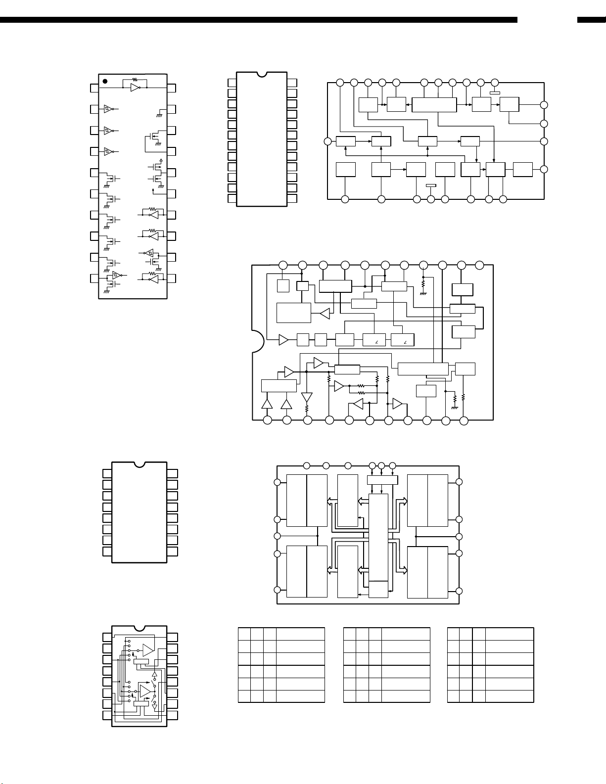
CXP82840-319Q Terminal Function
SEMICONDUCTORS
IC’s
CXP82840-319Q (IC900)
1 G2/A1 O FL G02
2 G1/A0 O FL G01
3 NC(Vdd) I NC(Connect to Vdd)
4 POWER DOWN I AC OFF Detect
5 ENC VOLUME UP I Encoder VOLUME UP
6 RDS CLOCK I RDS clock input(TDA7330)
7 ENC VOLUME DOWN I Encoder VOLUME DOWN
8 REMOCON I Remote signal input.
9 PROTECTION I Protection detecting input.
10 SUB ZONE2 LED O ZONE3 LED indicator control
11 SUB ZONE1 LED O ZONE2 LED indicator control
12 62446 LATCH O Electronic volume control.(M62446 LATCH)
13 FUNCTION SW 1 CE O Function IC control.(TC9274 CE)
14 FUNCTION 1/2 DATA O Function IC control.(TC9274 DATA)
15 FUNCTION 1/2 CLOCK O Function IC control.(TC9274 CLOCK)
16 VOLUME,PLL,4094,DATA O LC72131,M62446,KIC9459,TC9184,TC4094(DATA)
17 VOLUME,PLL,4094,CLOCK O LC72131,M62446,KIC9459,TC9184,TC4094(CLOCK)
18 TUNED I TUNED signal in.
19 STEREO I STEREO signal in.
20 IF COUNT I PLL data in.(LC72131)
21 TUNER MUTE O Tuner mute output.
22 PLL CE O LC72131(CE)
23 4094 STB O TC4094(STB)
24 VOLUME STB O KIC9459,TC9184(STB)
25 SUB 1 MUTE O ZONE2 mute control.
26 MAIN MUTE O MAIN,Subwoofer mute output.
27 POWER RELAY O Power supply relaycontrol.
28 AV REF. I Reference voltage input for A/D converter.
29 1511 DATA O Not used.
30 RDS DATA I Not used.
31 KEY IN 1 I Key input 1
32 KEY IN 2 I Key input 2
33 KEY IN 3 I Key input 3
34 STEP OPTION I Area select.
35 SET OPTION I Model select.
36 SPEAKER A LED 1 O SPEAKER A LED indicator control
37 A VSS I A/D converter GND.
38 RESET I Low-level active,system reset.
39 EXTAL I EXTAL(10MHz)
40 XTAL O XTAL(10MHz)
41 VSS I GND
42 NC(TX) O Not used.
43 G(TEX) I GND
44 VDD I Vcc SUPPLY.
45 VFDP I FDP voltage supply.
Pin
No. Pin Name FunctionI/O
Pin
No. Pin Name FunctionI/O
46 SPEAKER B LED 2 O SPEAKER B LED indicator control
47 STBY LED 3 O STANDBY LED indicator control
48 PD2/A53 O FL P38
49 PD3/A52 O FL P37
50 PD4/A51 O FL P36
51 PD5/A50 O FL P01
52 PD6/A49 O FL P02
53 PD7/A48 O FL P03
54 PF0/A47 O FL P04
55 PF1/A46 O FL P05
56 PF2/A45 O FL P06
57 PF3/A44 O FL P07
58 PF4/A43 O FL P08
59 PF5/A42 O FL P09
60 PF6/A41 O FL P10
61 PF7/A40 O FL P11
62 PG0/A39 O FL P12
63 PG1/A38 O FL P13
64 PG2/A37 O FL P14
65 PG3/A36 O FL P15
66 PG4/A35 O FL P16
67 PG5/A34 O FL P17
68 PG6/A33 O FL P18
69 PG7/A32 O FL P19
70 PH0/A31 O FL P20
71 PH1/A30 O FL P21
72 PH2/A29 O FL P22
73 PH3/A28 O FL P23
74 PH4/A27 O FL P24
75 PH5/A26 O FL P25
76 PH6/A25 O FL P26
77 PH7/A24 O FL P27
78 A23 O FL P28
79 A22 O FL P29
80 A21 O FL P30
81 A20 O FL P31
82 A19 O FL P32
83 A18 O FL P33
84 A17 O FL P34
85 A16 O FL P35
86 G16 O FL G16
87 G15 O FL G15
88 G14 O FL G14
89 Vdd I Vcc SUPPLY.
90 G13 O FL G13
91 G12 O FL G12
92 G11 O FL G11
93 G10 O FL G10
94 G9 O FL G09
95 G8 O FL G08
96 G7 O FL G07
97 G6 O FL G06
98 G5 O FL G05
99 G4 O FL G04
100 G3 O FL G03
8
DRA-395
1CXP82840.p65 01/08/18, 15:40Page 8-9 AdobePageMaker6.5J/Win

9
DRA-395
LA1266 (IC402)
10
4
13
8
19
15
17
18
14
21
22
GND
Vcc
5
11
IF
BUFFER
IF
BUFFER
2
FM - IF
6
Q.D.
7
REG
23
OSC
OSC
BUFFER
24
NARROW
S-METER S-METER
16
LED
DRIVER
RF MIX
12
20
AM-IF DET
AGC
POST
AMP
9
13
AM-IF FM-IF FM-IN
AM - I N
TC9184AP (IC602)
2
3
4
5
6
116 7 8
910
15
14
13
BASS+
BASS-
COM
TREBLE-
TREBLE+
V
SS
V
DD
GND
CK
DATA
STB
BASS+
BASS-
COM
TREBLE-
TREBLE+
Ladder resister
Analog switch
13 bit latch circuit
Level shift
20 bit Shift register circuit
Analog switch
Ladder resister
Ladder resister
Analog switch
13 bit latch circuit
Code
detect
circuit
Analog switch
Ladder resister
20
19
18
17 16 15 14 13 12
9
87
5
6
1
21
LA3401 (IC403)
22
VOL
REG OSC
SYMMETRICAL
REOCTANCE
CIRCUIT
PHASE
COMPARATOR
VCO STOP
PILOT DET
FF FF FF
38kHz
FF
38kHz 90°
FF
19kHz 90°
MUTING
FM AM CHANGE
Ro
Rc
Rc Rb
234
DECODER MUTING CONTROL
FM AM CHANGE OVER
Vcc ON
MUTING
MUTING
OUTPUT
STEREO
SWITCH
TRIGGER
LAMP
DRIVER
Rb
10 11
LC72131M (IC401)
120
219
318
417
516
615
714
813
912
10 11
XI N
CE
DI
CL
DO
BO1
BO2
BO3
BO4
IO1
AOUT
AI N
PD
V
DD
FMIN
AMI N
IO2
IFIN
Vss
XOUT
BA7625 (IC501)
1
2
3
4
5
6
7
8
16
15
14
13
12
11
10
9
Monitor OUT
GND
IN5
GND
IN4
CTL E
IN3
CTL D
IN1
CTL A
V OUT1
Vcc
IN2
CTL B
V OUT2
CTL C
6dB
6dB
LOGIC
LOGIC
ABE
MONITOR OUT
C D E V OUT 1 C D E V OUT 2
LL *IN 1 LL*
¾
LL *IN 1
HL *IN 2 HL*IN 2 HL *
¾
LH *IN 3 LH*IN 3 LH *IN 3
HH L IN4 HHL IN4 HH L IN4
HHH IN5 HHH IN5 HHH IN5
Note 1: * mark means that feasible for either H or L.
Note 2: Each input terminal is provided with sink chip clamp (BA7625).
Each input terminal takes 20kohm at the end (BA7626).
11
12
1
2
3
4
5
6
7
8
16
15
14
13
12
11
10
9
Vss
BASS
+
BASS
-
CON
TREBLE
-
TREBLE
+
GND
CK
VDD
BASS
+
BASS
-
COM
TREBLE
-
TREBLE
+
STB
DATA
1
2
3
4
5
6
7
8
9
10
11
12
24
23
22
21
20
19
18
17
16
15
14
13

10
DRA-395
ABLC
GND
Vcc
161
152
143
134
125
116
107
9
8
STR
D
CP
QP
0
QP
1
QP
4
QP
5
QP
6
QP
7
QS
2
QS
1
QP
3
QP
2
GND
OE
42
41
40
39
38
37
36
35
34
33
32
31
30
29
28
27
26
25
24
23
22
1
2
3
4
5
6
7
8
9
10
11
12
13
14
15
16
17
18
19
20
21
OUT4
OUT3
OUT2
OUT1
AV
DD
DV
DD
SW
OUT
SR
OUT
SL
OUT
C
OUT
R
OUT
L
OUT
AV
SS
SWin
GNDS
SRin
SLin
GNDC
Cin
DNDR
Rin
GNDL
Lin
BYPASSR
BLPASSL
LTRE
LBASS3
LBASS2
LBASS1
CLK
DATA
LATCH
DGND
AGND
CL1
CL2
CR1
CR2
RTRE
RBASS3
RBASS2
RBASS1
tone tone
OUTPUT
PORT
MCU
I/F
V
CC
VOUT
22kohm
B.P.F
PD
volume
volume
volume
volume
volume
volume
TC9274N-008 (IC303)
M62446FP (IC603)
PC74HC4094 (IC604)
ICP-N15 (IC105)
P43T7D330BW16
NJL64H380A(RMC900)
IC PROTECTOR
IR SENSOR
POSISTOR
Detector
Comparator
LimiterAmpHead Amp
FRONT VIEW
FRONT VIEW
Vout
GND
Vcc
FRONT VIEW
A OUTPUT
A –INPUT
A+INPUT
V
B OUTPUT
V
B –INPUT
B +INPUT
1
2
3
45
7
8
6
NJM2068DD (IC300 302, 605 610)
8
7
5
6
4
3
2
1
ABLC
Head
Amp
Limiter
Amp
+
–
IN
C1
C2 GNDfo NC
OUT
Vcc
CXA1511M(IC502)
81
72
63
54
IN
C1
C2
GND
NC
fo
OUT
V
CC
KIC9459F (IC601)
1
2
3
4
5
6
7
8
9
10
11
12
24
23
22
21
20
19
18
17
16
15
14
13
Vss
L-OUT
NC
L-IN
L-LD1
L-LD2
L.A.GND
NC
CS1
NC
GND
CK
VDD
R-OUT
NC
R-IN
R-LD1
R-LD2
R.A.GND
NC
CS2
NC
STB
DATA
L-ch R-ch
KIA7805AP (IC103)
NJM7805FA (IC104)
KIA7815AP (IC101)
NJM7915FA (IC102)
Input
GND
Output
FRONT
VIEW
GND
Input
Output
FRONT
VIEW
42
S1 41
S1S1 40
39
S1 38
S1
S1S1 37
S1 36
S7 35
S8 42
S1S5
34
S1 42
42
42
42
33
S10 32
S11 31
S12 30
42
42
42
42
S13 29
S14 28
S15 27
S16 26
42
42
42
42
S17 25
S18 24
23
22
STB
DATA
S9
S6
S1
S3
S4
S2
VDD
1
2
3
4
5
6
7
S78
S8
S5
9
10
S1011
S1112
S1213
S1314
S1415
S15
16
S1617
S1718
S1819
20
21
GND
CK
S9
S6
S1
S3
S4
S2
VSS
BPF
BEF
Detector &
Comparator Integrator Hysteresis
Comparator

11
DRA-395
2SD947F
KTA1266Y
KSA992F
KSC1845F
KTC3200BL
KTC3198Y
KTA1268BL
KSA916Y
2SC1740S
KTC2874B
KTC3880S
DTA114EK
DTA114YK
DTC114YK
TOP
VIEW
E
B
C
TOP
VIEW
E
B
C
FRONT
VIEW
B
C
E
TOP VIEW
KDS160MTZJ3.3B
MTZJ5.1B
MTZJ5.6B
MTZJ6.2B
MTZJ6.8B
MTZJ7.5A
MTZJ7.5B
MTZJ18B
MTZJ20B
1N4007
1SS133
B
C
E
R1
R2
B
C
E
R1
R2
2SB1560
2SD2390
FRONT
VIEW
ECB
DTA114ES
DTA144ES
DTC114ES
DTC114YS
DTC144ES
FRONT
VIEW
B
C
E
DTA series DTC series
DTA114EK
DTA114YK
R1
10kohm
R2
10kohm
10kohm 47kohm
DTA114ES 10kohm 10kohm
DTA114ES 47kohm 47kohm
DTC114YK
R1 R2
10kohm 47kohm
DTC144ES 47kohm 47kohm
DTC114YS 10kohm 47kohm
DTC114ES 10kohm 10kohm
TOP VIEW
HL-50RDRF4
KBPC604
TRANSISTORS
DIODES (LED Included)

12
DRA-395
FL DISPLAY
16-st-42GNK (FL900)
S38
S14
S9 S1
S2
S3
S4
S5
S12
S13
S7
S15
S6
S10
S11
G1
G1
G2
G3
G4
G5
G6
G7
G16 G15 G13 G12 G10 G9
F2F1
158
G14 G11 G8
G2~G16
12345
6
7 8 9 10111213141516171819
23 24 25
26
27 28 29 30 31 32 33 34
F1 F1 S1 S2 S3
S4
S5 S6 S7 S8 S9 S10 S11 S12 S13 S14 S15 S16 S17
20
21 22 35 36 37 38 39 40
41 42 43 44 45
46
47 48 49 50 51 52 53 54 55 56 57
S18
S19 S20 S21 S22 S23 S24 S25 S26 S27 S28 S29 S30 S31 S32 S33 S34 S35 S36 S37 S38
G16 G15 G14 G13 G12 G11 G10 G9 G8 G7 G6 G5 G4 G3 G2 G1 F2 F2
58
F1,F2 : Filament
G1~G16 : Grid
S1~S38 : Anode
S13
S14
S15
S16
S17
S18
S19
S20
S21
S22
S23
S24
G1 G2 G3 G4 G5 G6 G7 G8 G9 G10 G11 G12 G13 G14 G15 G16
S38
S36
S37
S38
-2
DBS
TV
-1
VDP
TAPE
//(DVD)
/(MD)
AUX
DVD
MD V.AUX
TUNER
-2
-3
CD
-1
PHONO
VCR
REC
MULTI
STEREO
AUTO
TUNED
RDS
CH
S1
S2
S3
S4
S5
S6
S7
S8
S9
S10
S11
S12
S1
S2
S3
S4
S5
S6
S7
S9
S10
S11
S12
S1
S2
S3
S4
S5
S6
S7
S8
S9
S10
S11
S12
S13
S14
S15
S16
S17
S18
S19
S20
S21
S22
S23
S24
S13
S14
S15
S25
S26
S27
S28
S29
S30
S31
S32
S33
S34
S35
S25
S26
S27
S28
S29
S30
S31
S32
S33
S34
S35
G2~G16
G1
G2~G16
G1
G2~G16
G1
G2~G16
G1
DIGITAL
PRO LOGIC
S1
S6
S11
S16
S21
S26
S31
S2
S7
S12
S17
S22
S27
S32
S3
S8
S13
S18
S23
S28
S33
S4
S9
S14
S19
S24
S29
S34
S5
S10
S15
S20
S25
S30
S35
TUNED
RDS
STEREO
AUTO
REC
MULTI
PHONO
VCR
CD
-
1
TUNER
-
2
-
3 V.AUX
AUX
MD
DVD /
/TAPE
VDP TV
-
1
-
2
/DBS
PRO LOGIC
DIGITAL
DIGITAL
ANALOG
TUNED
RDS
STEREO
AUTO
REC
MULTI
PHONO
VCR
CD
-1
TUNER
-2-3V.AUX
AUX
MD
DVD /
/TAPE
VDP TV
-1-2
/ DBS
CH
CH
PRO LOGIC
DIGITAL
DIGITAL
ANALOG
Pin Assignment
Anode & Grid Assignment
PIN NO.
CONNECTION
PIN NO.
CONNECTION
PIN NO.
CONNECTION

18
DRA-395
tttt
ll
ll
lResistors
Ex.:RN 14K 2E 182 GFR
Type Shape Power Resist- Allowable Others
and per- ance error
formance
tt
tt
s
s
s
s
Resistance
1 8 2⇒1800 ohm = 1.8 kohm
Indicates number of zeros after effective number.
2-digit effective number.
•Units: ohm
1 R 2⇒1.2 ohm
1-digit effective number.
2-digit effective number, decimal point indicated by R.
•Units: ohm
ll
ll
lCapacitors
Ex.:CE 04W 1H 2R2 MBP
Type Shape Dielectric Capacity Allowable Others
and per- strength error
formance
s
s
s
s
ss
Capacity (electrolyte only)
2 2 2⇒2200µF
Indicates number of zeros after effective number.
2-digit effective number.
•Units: µF.
2 R 2⇒2.2µF
1-digit effective number.
2-digit effective number, decimal point indicated by R.
•Units: µF.
Capacity (except electrolyte)
2 2 2⇒2200pF=0.0022µF
(More than 2) Indicates number of zeros after effective number.
2-digit effective number.
•Units: pF.
2 2 1⇒220pF
(0 or 1) Indicates number of zeros after effective number.
2-digit effective number.
•Units: pF.
•When the dielectric strength is indicated in AC, "AC" is included after the dieelectric
strength value.
ss
NOTE FOR PARTS LIST
lPart indicated with the mark "" are not always in stock and possibly to take a long period of time for supplying, or in
some case supplying of part may be refused.
lWhen ordering of part, clearly indicate "1" and "I" (i) to avoid mis-supplying.
lOrdering part without stating its part number can not be supplied.
lPart indicated with the mark " " is not illustrated in the exploded view.
lNot including Carbon Film ±5%, 1/4W Type in the P.W.Board parts list. (Refer to the Schematic Diagram for those parts.)
WARNING:
Parts marked with this symbol have critical characteristics.
Use ONLY replacement parts recommended by the manufacturer.
RD : Carbon 2B : 1/8W F : ±1% P : Pulse-resistant type
RC : Composition 2E : 1/4W G : ±2% NL : Low noise type
RS : Metal oxide film 2H : 1/2W J : ±5% NB : Non-burning type
RW : Winding 3A : 1W K : ±10% FR : Fuse-resistor
RN : Metal film 3D : 2W M : ±20% F : Lead wire forming
RK : Metal mixture 3F : 3W
3H : 5W
CE : Aluminum foil 0J : 6.3V F : ±1% HS : High stability type
electrolytic
CA : Aluminum solid 1A : 10V G : ±2% BP : Non-polar type
electrolytic
CS : Tantalum electrolytic 1C : 16V J : ±5% HR : Ripple-resistant type
CQ : Film 1E : 25V K : ±10% DL : For change and discharge
CK : Ceramic 1V : 35V M : ±20% HF : For assuring high
requency
CC : Ceramic 1H : 50V Z : +80% U : UL part
CP : Oil 2A : 100V –20% C : CSA part
CM : Mica 2B : 125V P : +100% W : UL-CSA type
CF : Metallized 2C : 160V –0% F : Lead wire forming
CH : Metallized 2D : 200V C : ±0.25pF
2E : 250V D : ±0.5pF
2H : 500V = : Others
2J : 630V

19
DRA-395
PARTS LIST OF P.W.B. UNIT
MAIN P.W.B. UNIT ASS'Y
Ref. No. Part No. Part Name Remarks Ref. No. Part No. Part Name Remarks
SEMICONDUCTORS GROUP
IC101 963 0057 903 IC KIA7815AP J126781500060
IC102 963 0044 806 IC NJM7915FA J126791500010
IC103 960 0057 709 IC KIA7805AP J126780500360
IC104 960 0196 001 IC NJM7805FA J126780500130
IC105 960 0195 808 IC ICP-N15 J120001500030
IC300-302 960 0179 701 IC NJM2068DD J121206800000
IC303 963 0071 400 IC TC9274N-008 J080927400010
Q101,102 960 0196 603 Transistor KTC2874B J502287400010
Q103-106 960 0196 205 Transistor KSA992Y J5000992F0050
Q107,108 960 0196 506 Transistor KSC1845F J5021845F0000
Q115,116 960 0196 506 Transistor KSC1845F J5021845F0000
Q117-119 963 0022 006 Transistor DTC114YS J6020114Y0050
Q120 960 0196 302 Transistor KTA1268BL J5001268B0050
Q121 960 0196 700 Transistor KTC3200BL J5023200B0050
Q122 960 0189 005 Transistor KSA916Y J5000916Y0050
Q123 960 0005 105 Transistor KTA1266Y J5001266Y0050
Q124 960 0005 202 Transistor KTC3198Y J5023198Y0000
Q125 960 0196 302 Transistor KTA1268BL J5001268B0050
Q126,127 960 0005 202 Transistor KTC3198Y J5023198Y0000
Q128 960 0196 302 Transistor KTA1268BL J5001268B0050
Q129,130 960 0005 202 Transistor KTC3198Y J5023198Y0000
Q131,132 960 0196 302 Transistor KTA1268BL J5001268B0050
Q133,134 960 0196 409 Transistor 2SC1740SR J5021740S0010
Q136 963 0022 006 Transistor DTC114YS J6020114Y0050
D101-113 963 0020 309 Diode 1SS133 K000013300520
D114-119 963 0058 407 Diode 1N4007 K000400700520
D120,121 963 0020 309 Diode 1SS133 K000013300520
D122-125 963 0058 407 Diode 1N4007 K000400700520
D126-129 963 0020 309 Diode 1SS133 K000013300520
D130,131 963 0058 407 Diode 1N4007 K000400700520
D132-135 963 0020 309 Diode 1SS133 K000013300520
DB101,102 960 0197 107 Diode KBPC604 K047604000020
DZ101,102 963 0046 202 Zener diode MTZJ18B K06018R044520
DZ103,104 963 0047 405 Zener diode MTZJ7.5B K06007R544520
DZ105 963 0058 708 Zener diode MTZJ20B K06020R044520
DZ106 960 0095 500 Zener diode MTZJ5.1B K06005R144520
DZ107-110 963 0047 502 Zener diode MTZJ3.3B K06003R344520
RESISTORS GROUP
R117,118 960 9004 301 Metal film 47ohm 1/4W (NB) C060047063050
R127-130 244 2052 957 Metal film 5.6kohm 1W (NB) C060056265070
R135,136 963 9003 068 Metal film 4.7ohm 1/4W (NB) C0604R7063050
R137-140 244 2043 982 Metal film 0.22ohm 1W (NB) C060R22065070
R141,142 963 9003 068 Metal film 4.7ohm 1/4W (NB) C0604R7063050
R143-146 244 2043 982 Metal film 0.22ohm 1W (NB) C060R22065070
R153-156 244 2043 937 Metal oxide 10ohm 1W (NB) C041010065060
R162-164 244 2055 996 Metal film 1.2kohm 1W (NB) C060012265050
R165 244 2043 937 Metal oxide 10ohm 1W (NB) C041010065060
R166 244 2043 982 Metal film 0.22ohm 1W (NB) C060R22065050
R173 963 9003 068 Metal film 4.7ohm 1/4W (NB) C0604R7063050
R190,191 963 0045 203 Winding 0.1ohm 5W C144R10069110
R195-197 244 2043 982 Metal film 0.22ohm 1W (NB) C060R22065050
R201 244 2043 982 Metal film 0.22ohm 1W (NB) C060R22065050
R208 963 9005 105 Carbon film 68ohm 1/4W C000068063520
R209 963 0043 108 Metal film 2.2Mohm 1/2W C060022574000
VR101,102 960 0091 601 Semi fixed resistor 1kohm C544102015130
CAPACITORS GROUP
C101,102 Electrolytic 22uF/50V D040220087060
C103,104 Electrolytic 10uF/50V D040100087070
C105,106 963 9005 118 Ceramic 100pF/50V D004101067060
C107,108 963 9003 165 Ceramic 220pF/500V D009092212500
C109,110 Electrolytic 47uF/25V D040470084070
C111,112 963 9005 121 Ceramic 33pF/500V D00033006D050
C115,116 963 9005 134 Ceramic 1200pF/50V D004122287050
C117,118 Electrolytic 47uF/50V D040470087060
C119,120 963 9003 084 Ceramic 100pF/500V D00410106D050
C121,122 Electrolytic 10uF/50V D040100087070
C123,124 963 9003 084 Ceramic 100pF/500V D00410106D050
C125,126 963 9004 517 Ceramic 0.022uF/50V D004223597050
C127-130 963 9003 097 Mylar film 0.1uF/250V D02010407H080
C135 963 9004 504 Ceramic 0.01uF/50V D004103097060
C136 Electrolytic 2.2uF/50V D0402R2087100
C137 963 9004 504 Ceramic 0.01uF/50V D004103097060
C138,139 Electrolytic 1uF/50V D040010087080
C140 963 9005 147 Ceramic 0.1uF/25V D004104594050
C141 Electrolytic 220uF/6.3V D040221081230
C142 963 9005 147 Ceramic 0.1uF/25V D004104594050
C143 Electrolytic 220uF/6.3V D040221081230
C144,145 963 9005 260 Electrolytic 8200uF/63V D040822088030
C146-150 963 9003 097 Mylar film 0.1uF/250V D02010407H080
C151 Electrolytic 1uF/50V D040010087080
C152 963 9005 163 Electrolytic 1000uF/50V D040102087080
C153-155 963 0021 900 Mylar film 0.047uF/100V D02047306C060
C156 960 9007 201 Electrolytic 3300uF/35V D040332085010
C157 963 9003 123 Electrolytic 1000uF/35V D040102085040
C158-161 Electrolytic 10uF/50V D040100087070
C162 Electrolytic 4.7uF/50V D0404R7087100
C164 963 9003 136 Electrolytic 1000uF/25V D040102084060
C167,168 Electrolytic 1uF/50V D040010087080
C169 963 9005 176 Ceramic 4700pF/250V (AC) D008472089010
C170 963 9005 299 Electrolytic 100uF/100V D04010108C200
C171,172 963 0021 900 Mylar film 0.047uF/100V D02047306C060
C173 963 9005 286 Electrolytic 3300uF/16V D040332083100
C174 Electrolytic 10uF/50V D040100087070
C176 963 0021 900 Mylar film 0.047uF/100V D02047306C060

20
DRA-395
Ref. No. Part No. Part Name Remarks Ref. No. Part No. Part Name Remarks Q'ty
C301 Electrolytic 10uF/50V D040100087050
C302,303 963 9005 273 Ceramic 220pF/50V D004221067060
C304 Electrolytic 10uF/50V D040100087050
C307,308 Electrolytic 220uF/6.3V D040221081050
C311,312 963 9005 118 Ceramic 100pF/50V D004101067060
C313,314 963 9004 779 Mylar film 0.024uF/50V D020243167050
C315,316 960 9008 695 Mylar film 6800pF/100V D02068206C060
C317,318 Electrolytic 4.7uF/50V D0404R7087250
C319,320 963 9004 517 Mylar film 0.022uF/50V D004223597050
C321-324 Electrolytic 47uF/25V D040470084100
C325,326 963 9005 118 Ceramic 100pF/50V D004101067060
C327,328 Electrolytic 4.7uF/50V D0404R7087250
C329,330 Electrolytic 10uF/50V D040100087050
C331,332 963 9005 118 Ceramic 100pF/50V D004101067060
C333,334 Electrolytic 4.7uF/50V D0404R7087250
C335,336 963 9005 118 Ceramic 100pF/50V D004101067060
C337,338 Electrolytic 10uF/50V D040100087050
C339-344 963 9005 118 Ceramic 100pF/50V D004101067060
C347-349 Electrolytic 1uF/50V D040010087080
OTHER PARTS GROUP Q'ty
CN600 963 0086 709 11P connector base L101100031110 1
CN601 963 0085 700 6P connector base L101100030610 1
CP101 960 0197 505 2P connector base L108202000220 1
CP102 960 0123 304 2P connector base L104353280200 1
CP103 963 0081 403 4P connector base L104353280400 1
CP104 960 0128 804 6P connector base L102526700600 1
CP107 960 0123 207 3P connector base L102526700300 1
CP608 963 0088 008 10P connector base L101100041010 1
CP609 963 0087 805 11P connector base L101100041110 1
CP907 963 0048 909 3P connector base L101220030000 1
F101 960 0188 705 Fuse 8A/125V G650802121060 1
F102 963 0089 803 Fuse 6.3A/125V G650632121150 1
F101A,B 960 0005 804 Fuse clip G645000050010 2
F102A,B 960 0005 804 Fuse clip G645000050010 2
GND101,102
960 9006 600 GND terminal 3790040876010 2
JACK102 963 0074 009 8P speaker terminal G61408103610A 1
JACK104 960 0181 508 2P AC outlet G435204004010 1
JACK301 960 0188 307 6P pin jack G603060610010 1
JACK302 960 0188 200 4P pin jack G602040610000 1
JACK303 960 0188 307 6P pin jack G603060610010 1
L101,102 963 0049 005 Inductor 0.5uH D330R50000000 2
RLY101 960 0181 702 Relay (G5PA-28) G680240502020 1
RLY102 963 0071 303 Relay (RSB24S) G680240202010 1
RLY103 960 0181 702 Relay (G5PA-28) G680240502020 1
RLY104 960 0181 605 Relay (G5PA-1-8) G680120502010 1
T101 960 0185 708 Power trans. (Sub) 8200280960010 1
TP101,102 960 0161 405 3P connector base L101530140310 2
Heat sink 2120043538050 1
963 0018 007 Screw 3
×
8 (B)-Z B020030081B10 2
963 0090 009 Shield plate 3070210146000 1
Other manuals for DRA-395
4
Table of contents
Other Denon Stereo Receiver manuals

Denon
Denon AVR-1907 User manual

Denon
Denon AVR-791 User manual

Denon
Denon AVR-2309CI User manual

Denon
Denon AVR-S740H User manual

Denon
Denon AVR-X2500H User manual

Denon
Denon AVR-X8500H Quick start guide

Denon
Denon AVR-3808CI User manual

Denon
Denon AVR-2807 User manual

Denon
Denon AVR-E300P User manual

Denon
Denon AVR-1708 User guide

Denon
Denon AVR-1706 User manual

Denon
Denon AVRX1500HOM User manual

Denon
Denon AVR-1508 User manual

Denon
Denon AVR-1603 User manual

Denon
Denon AVR-3310CI User manual

Denon
Denon AVR-S950H Series User manual

Denon
Denon AVR-X520BT User manual

Denon
Denon AVR 2807 - AV Receiver Instruction Manual

Denon
Denon AVR-983 User manual

Denon
Denon AVR-X4200W User manual