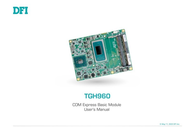
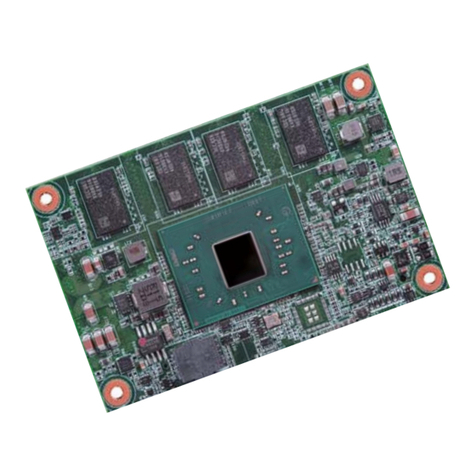
DFI EHL9A2 Guide

EHL9A2
COM Express Mini Module
Carrier Board Design Guide
© May 04, 2023 DFI Inc.

2Design Guide | EHL9A2
Copyright
This publication contains information that is protected by copyright. No part of it may be re-
produced in any form or by any means or used to make any transformation/adaptation with-
out the prior written permission from the copyright holders.
This publication is provided for informational purposes only. The manufacturer makes no rep-
resentations or warranties with respect to the contents or use of this manual and specifically
disclaims any express or implied warranties of merchantability or fitness for any particular
purpose. The user will assume the entire risk of the use or the results of the use of this docu-
ment. Further, the manufacturer reserves the right to revise this publication and make changes
to its contents at any time, without obligation to notify any person or entity of such revisions
or changes.
Changes after the publication’s first release will be based on the product’s revision. The web-
site will always provide the most updated information.
© 2023. All Rights Reserved.
Trademarks
Product names or trademarks appearing in this manual are for identification purpose only and
are the properties of the respective owners.
COM Express Specification Reference
PICMG® COM Express® Module Base Specification.
http://www.picmg.org/
FCC and DOC Statement on Class B
This equipment has been tested and found to comply with the limits for a Class B digital
device, pursuant to Part 15 of the FCC rules. These limits are designed to provide reason-
able protection against harmful interference when the equipment is operated in a residential
installation. This equipment generates, uses and can radiate radio frequency energy and, if not
installed and used in accordance with the instruction manual, may cause harmful interference
to radio communications. However, there is no guarantee that interference will not occur in a
particular installation. If this equipment does cause harmful interference to radio or television
reception, which can be determined by turning the equipment off and on, the user is encour-
aged to try to correct the interference by one or more of the following measures:
• Reorient or relocate the receiving antenna.
• Increase the separation between the equipment and the receiver.
• Connect the equipment into an outlet on a circuit different from that to which the re-
ceiver is connected.
• Consult the dealer or an experienced radio TV technician for help.
Notice:
• The changes or modifications not expressly approved by the party responsible for
compliance could void the user’s authority to operate the equipment.
• Shielded interface cables must be used in order to comply with the emission limits.

3Design Guide | EHL9A2
Table of Contents
Chapter 1 - Introduction................................................................................................................6
COM Express Overview..........................................................................................................6
Specification ........................................................................................................................... 7
Block Diagram ........................................................................................................................ 9
Board Layout .......................................................................................................................10
System Memory ..................................................................................................................10
Terminology .........................................................................................................................11
Chapter 2 - Concept....................................................................................................................12
COM Express Module Standards .......................................................................................12
Chapter 3 - Carrier Board Schematic Guidelines......................................................................13
PCI Express Bus ..................................................................................................................13
Serial ATA .............................................................................................................................16
Gigabit Ethernet (GBE).........................................................................................................18
HD Audio...............................................................................................................................23
Universal Serial Bus 2.0 and 3.1 (USB 2.0 and 3.1) ..........................................................27
LVDS ......................................................................................................................................32
Digital Display Interface.......................................................................................................36
Miscellaneous.......................................................................................................................42

4Design Guide | EHL9A2
About this Manual
This manual can be downloaded from the website.
The manual is subject to change and update without notice, and may be based on editions
that do not resemble your actual products. Please visit our website or contact our sales repre-
sentatives for the latest editions.
Warranty
• Warranty does not cover damages or failures that occur from misuse of the product,
inability to use the product, unauthorized replacement or alteration of components
and product specifications.
• The warranty is void if the product has been subjected to physical abuse, improper
installation, modification, accidents or unauthorized repair of the product.
• Unless otherwise instructed in this user’s manual, the user may not, under any cir-
cumstances, attempt to perform service, adjustments or repairs on the product,
whether in or out of warranty. It must be returned to the purchase point, factory or
authorized service agency for all such work.
• We will not be liable for any indirect, special, incidental or consequential damages to
the product that has been modified or altered.
Static Electricity Precautions
It is quite easy to inadvertently damage your PC, system board, components or devices even
before installing them in your system unit. Static electrical discharge can damage computer
components without causing any signs of physical damage. You must take extra care in han-
dling them to ensure against electrostatic build-up.
• To prevent electrostatic build-up, leave the system board in its anti-static bag until
you are ready to install it.
• Wear an antistatic wrist strap.
• Do all preparation work on a static-free surface.
• Hold the device only by its edges. Be careful not to touch any of the components,
contacts or connections.
• Avoid touching the pins or contacts on all modules and connectors. Hold modules or
connectors by their ends.
Safety Measures
• To avoid damage to the system, use the correct AC input voltage range.
• To reduce the risk of electric shock, unplug the power cord before removing the sys-
tem chassis cover for installation or servicing. After installation or servicing, cover
the system chassis before plugging the power cord.
Important:
Electrostatic discharge (ESD) can damage your processor, disk drive and other
components. Perform the upgrade instruction procedures described at an ESD
workstation only. If such a station is not available, you can provide some ESD
protection by wearing an antistatic wrist strap and attaching it to a metal part of
the system chassis. If a wrist strap is unavailable, establish and maintain contact
with the system chassis throughout any procedures requiring ESD protection.

5Design Guide | EHL9A2
About the Package
The package contains the following items. If any of these items are missing or damaged,
please contact your dealer or sales representative for assistance.
The accessories in the package may not come similar to the information listed below. This may
differ in accordance with the sales region or models in which it was sold. For more information
about the standard package in your region, please contact your dealer or sales representative.
• Heat Sink (For IHS package CPU)
• Heat Sink (For BARE-DIE CPU)
• Cooler (For IHS packages CPU with wide temperature environment.)
* IHS : Integrated Heat Spreader
Optional Items
The board and accessories in the package may not come similar to the information listed
above. This may differ in accordance with the sales region or models in which it was sold. For
more information about the standard package in your region, please contact your dealer or
sales representative.
Before Using the System Board
Before using the system board, prepare basic system components.
If you are installing the system board in a new system, you will need at least the following
internal components.
• Storage devices such as hard disk drive, etc.
You will also need external system peripherals you intend to use which will normally include
at least a keyboard, a mouse and a video display monitor.

6
Chapter 1
INTRODUCTION
Design Guide | EHL9A2
Chapter 1 - Introduction
XCOM Express Overview
This design guide addendum organizes and provides the recommendations of DFI’s COM car-
rier board design for COM-Express Modules. All other Schematic Guidelines for the carrier
board are applicable and can be found in the PICMG Design Guide V1.0. Please contact DFI
sales and application engineers if there are any questions about designing the carrier board,
or you plan to use this processor in applications other than mobile or desktop platforms.
COM Express complies with COM Express standard from the PCI Industrial Computer Manu-
facturers Group (PICMG) which provides next-generation performance of the smallest state
in the art of embedded modules. DFI’s COM Design Support Services (CDSS) help customers
develop and integrate their carrier boards with DFI’s COM modules. CDSS provides a series
of valuable services such as Product, Design Assistance, Software and Thermal Solution ser-
vices, together they help reduce risks when designing carrier boards. For more details, please
visit at “http://www.dfi.com” DFI offers a wide range of COM products to cater to various
customers’ demands. The modular designs add more flexibilities to the system. The COM Ex-
press form factor allows the COM Express Modules to be easily and securely mounted on a
customized solution board. The design and multiple processor choices eliminate CPU integra-
tion worries and allow fast applications supporting for the most dynamic embedded needs.
Mini
Carrier Board
Compact
Basic
COM Express
Carrier Board
COMs are widely used by modular CPU boards with high-integration features.
COM-Express supports a wide range of processors and chipsets. They utilize specialized
technologies, including PCI Express, Serial ATA, USB 2.0, etc. Not only do COMs allow quick
design, they also provide the benefits of easy installation, maintenance and upgrade ease.
Though small in size, COMs implement CPU architectures and basic common circuits.
Many system integrators find that DFI COM solutions have already covered around 80%
of their feature requirements. This makes COM products powerful and cost-efficient.
Carrier board
COM Express Mini Module

7
Chapter 1
INTRODUCTION
Design Guide | EHL9A2
XSpecification
SYSTEM Processor Intel Atom®x6000 series and Intel®Celeron®and Pentium®N & J series processors (formerly Code name “Elkhart Lake”)
Memory LPDDR4X max up to 16GB within dual channel and maximum speed depends on SOC.
(The LPDDR4X speed ≤ 3733 MT/s (2RPC/1RPC) and 4267 MT/s (1RPC) which depends on processor.)
Note:
• 8GB/16GB supported by project basis.
• In-band ECC (IBECC) with normal memory chip support on selected ATOM x6000 series SKUs.
IBECC can set enabled or disabled in BIOS setup menu.
BIOS AMI SPI 256Mbit
GRAPHICS Controller Intel®HD Graphics
Feature OpenGL 4.5, DirectX 12, OpenCL 1.2
HW Decode: AVC/H.264, MPEG2, VC1, WMV9, JPEG/MJPEG, HEVC/H.265, VP8, VP9, MVC
HW Encode: AVC/H.264, JPEG/MJPEG, HEVC/H.265, VP9, MVC
Display 1 x DDI
1 x LVDS/eDP
LVDS: single channel 24-bit, resolution up to 1920x1200 @ 60Hz
eDP: resolution up to 4096x2160 @ 60Hz
HDMI: resolution up to 4096x2160 @ 30Hz
DP++: resolution up to 4096x2160 @ 60Hz, 3840x2160 @60Hz
EXPANSION Interface 4 x PCIe x1 (Gen 3)
1 x SD/SDIO (available upon request)
1 x I2C
1 x SMBus
1 x LPC
1 x Speaker
1 x SPI
2 x UART (TX/RX)
AUDIO Interface HD Audio
ETHERNET Controller 1 x Intel®I225IT / I225-LM (10/100/1000Mbps/2.5Gbps)
I/O USB 2 x USB 3.1 Gen2
8 x USB 2.0
SATA 2 x SATA 3.0 (up to 6Gb/s)
eMMC 1 x 8GB/16GB/32GB/64GB*/128GB eMMC 5.1 (available upon request)
DIO 1 x 8-bit DIO

8
Chapter 1
INTRODUCTION
Design Guide | EHL9A2
WATCHDOG TIMER Output & Interval System Reset, Programmable via Software from 1 to 255 Seconds
SECURITY TPM dTPM or fTPM (Opational)
Power Type 4.75V~20V, 5VSB, VCC_RTC (ATX mode)
4.75V~20V, VCC_RTC (AT mode)
Consumption TBD
OS SUPPORT OS Support (UEFI
Only) Windows: Windows 10 IoT Enterprise 64-bit
Linux
ENVIRONMENT Temperature Operating: -5 to 65°C, -40 to 85°C
Storage: -40 to 85°C
Humidity Operating: 5 to 90% RH
Storage: 5 to 90% RH
MTBF TBD
MECHANICAL Dimensions COM Express® Mini 84mm (3.3") x 55mm (2.16")
Compliance PICMG COM Express® R3.0, Type 10
STANDARDS AND CER-
TIFICATIONS
Certification CE, FCC

9
Chapter 1
INTRODUCTION
Design Guide | EHL9A2
XBlock Diagram

10
Chapter 1
INTRODUCTION
Design Guide | EHL9A2
XBoard Layout
TOP VIEW
1
LPDDR4XLPDDR4X
LPDDR4X
SPI
LPDDR4X
COM Express connector
1
EMMC
BOTTOM VIEW
Important:
Boards, and other components. Perform installation procedures at an ESD work-
station only. If such a station is not available, you can provide some ESD protec-
tion by wearing an antistatic wrist strap and attaching it to a metal part of the
system chassis. If a wrist strap is unavailable, establish and maintain contact with
the system chassis throughout any procedures requiring ESD protection.
XSystem Memory
1
LPDDR4XLPDDR4X
LPDDR4X
SPI
LPDDR4X
The system board is equipped with LPDDR4X memory chips onboard.

11
Chapter 1
INTRODUCTION
Design Guide | EHL9A2
XTerminology
Conventions and Terminology
BTB Board to board COMe connector
COM A serial port interface on IBM PC-compatible computers running
Microsoft Windows or MS-DOS
COM-Express New generation technology of Computer On Module
CPU Central Processing Unit
CRT Cathode Ray Tube
LPDDR4/4X Low Power Double Data Rate IV SDRAM memory technology
DVI Digital Visual Interface
DVO Digital Video Out
EMI Electromagnetic Interference
ESD Electrostatic Discharge
FSB Front Side Bus, synonymous with Host or CPU bus
PCH Refers to the Peripheral Component Interface (PCI) Controller Hub
HD Audio High Denition Audio
I2CInter-IC (a two wire serial bus created by Philips)
IDE (ATA) Integrated Drive Electronics (Advanced Technology Attachment)
INTx An interrupt request signal where x stands for interrupts A, B, C,
and D
LAN A local area network (LAN) is a computer network covering a small
physical area
LCD Liquid Crystal Display
LPC The Low Pin Count (LPC) Interface Specication for legacy I/O has
facilitated the industry's transition toward ISA-less systems
LVDS LCD Low Voltage Dierential Signaling: A high speed, low power data
transmission standard used for display connections to LCD panels
MCH Refers to the Memory Controller Hub chipset component
NTSC National Television Standards Committee
PAL Phase Alternate Line
PCI Peripheral Component Interface
PCI-Express New generation PCI interface with serial interconnection technology
RTC Real Time Clock
SATA Serial ATA interface
SMBus System Management Bus
TMDS Transition Minimized Dierential Signaling
TV Television supports NTSC and PAL
UART A universal asynchronous receiver/transmitter that translates data
between parallel and serial forms.
USB Universal Serial Bus

12
Chapter 2
CONCEPT
Design Guide | EHL9A2
Chapter 2 - Concept
106.00
91.00
70.00
51.00
4.00
18.00
6.00
0.00
16.50
4.00
0.00
Extended
BasicCompact
Mini
74.20
80.00
91.00
121.00
151.00
Common for all Form Factors
Extended only
Basic only
Compact only
Compact and Basic only
Mini only
XCOM Express Module Standards
The figure below shows the dimensions of the different types of COM Express modules.
EHL9A2 is a COM Express Mini. The dimension is 84mm x 55mm.

13
Chapter 3
CARRIER BOARD SCHEMATIC GUIDELINES
Design Guide | EHL9A2
Chapter 3 - Carrier Board Schematic Guidelines
XPCI Express Bus
Signal Pin# Pin Type Pwr Rail /Tolerance EHL9A2 PU/PD Module Base Specification R3.0 Description COM Express Carrier Design Guide R2.0 Description
PCIE_TX0+ A68 AC Coupling capacitor
PCIE_TX0- A69 AC Coupling capacitor
PCIE_RX0+ B68
PCIE_RX0- B69
PCIE_TX1+ A64 AC Coupling capacitor
PCIE_TX1- A65 AC Coupling capacitor
PCIE_RX1+ B64
PCIE_RX1- B65
PCIE_TX2+ A61 AC Coupling capacitor
PCIE_TX2- A62 AC Coupling capacitor
PCIE_RX2+ B61
PCIE_RX2- B62
PCIE_TX3+ A58 AC Coupling capacitor
PCIE_TX3- A59 AC Coupling capacitor
PCIE_RX3+ B58
PCIE_RX3- B59
PCIE_CLK_REF+ A88
PCIE_CLK_REF- A89
Note: For PCIe device down or slot card components on the carrier board, please use the PCIe Lane0 port first.
Signal Pin# Pin Type Pwr Rail /Tolerance EHL9A2 PU/PD Module Base Specification R3.0 Description COM Express Carrier Design Guide R2.0 Description
USB0+ A46 USB Port 0, data + or D+
USB0- A45 USB Port 0, data - or D-
USB1+ B46 USB Port 1, data + or D+
USB1- B45 USB Port 1, data - or D-
USB2+ A43 USB Port 2, data + or D+
USB2- A42 USB Port 2, data - or D-
USB3+ B43 USB Port 3, data + or D+
USB3- B42 USB Port 3, data - or D-
USB4+ A40 USB Port 4, data + or D+
USB4- A39 USB Port 4, data - or D-
USB5+ B40 USB Port 5, data + or D+
USB5- B39 USB Port 5, data - or D-
USB6+ A37 USB Port 6, data + or D+
USB6- A36 USB Port 6, data - or D-
USB7+ B37 USB Port 7, data + or D+
USB7- B36 USB Port 7, data - or D-
USB_0_1_OC# B44 I CMOS 3.3V Suspend/3.3V PU 10Kto 3.3V Suspend
USB over-current sense, USB channels 0 and 1.
A pull-up for this line shall be present on the Module.
An open drain driver from a USB current monitor on the Carrier Board
may drive this line low.
Do not pull this line high on the Carrier Board.
USB over-current sense, USB ports 0 and 1.
Do not pull up these lines to 3.3V on the Carrier Board – this shall be
done on the Module.
I/O USB 3.3V Suspend/3.3V USB differential pairs, channel 6. If implemented, shall be host ports.
I/O USB 3.3V Suspend/3.3V USB differential pairs, channel 7. If implemented, shall be host ports.
I/O USB 3.3V Suspend/3.3V USB differential pairs, channel 4. If implemented, shall be host ports.
I/O USB 3.3V Suspend/3.3V USB differential pairs, channel 5. If implemented, shall be host ports.
I/O USB 3.3V Suspend/3.3V USB differential pairs, channel 2. If implemented, shall be host ports.
I/O USB 3.3V Suspend/3.3V USB differential pairs, channel 3. If implemented, shall be host ports.
USB Si
g
nals Descri
p
tions
I/O USB 3.3V Suspend/3.3V USB differential pairs, channel 0. If implemented, shall be host ports.
I/O USB 3.3V Suspend/3.3V USB differential pairs, channel 1. If implemented, shall be host ports.
I PCIE AC coupled off Module PCI Express Differential Receive Pairs 3 PCIe channel 3. Receive Input differential pair.
O PCIE PCIE Reference clock output for all PCI Express and PCI Express Graphics
lanes.
PCIe Reference Clock for all COM Express PCIe lanes, and for PEG
lanes.
I PCIE AC coupled off Module PCI Express Differential Receive Pairs 2 PCIe channel 2. Receive Input differential pair.
O PCIE AC coupled on Module PCI Express Differential Transmit Pairs 3 PCIe channel 3. Transmit Output differential pair.
I PCIE AC coupled off Module PCI Express Differential Receive Pairs 1 PCIe channel 1. Receive Input differential pair.
O PCIE AC coupled on Module PCI Express Differential Transmit Pairs 2 PCIe channel 2. Transmit Output differential pair.
I PCIE AC coupled off Module PCI Express Differential Receive Pairs 0 PCIe channel 0. Receive Input differential pair.
O PCIE AC coupled on Module PCI Express Differential Transmit Pairs 1 PCIe channel 1. Transmit Output differential pair.
PCI Ex
p
ress Lanes Si
g
nals Descri
p
tions
O PCIE AC coupled on Module PCI Express Differential Transmit Pairs 0 PCIe channel 0. Transmit Output differential pair.
Signal Description
The table listed below illustrates the signal descriptions of PCI Express Bus, including the following information:
Signal: signal name
Pin: pin number
Pin Type: the methods of transmission and reception
I input to the Module
O output from the Module
I/O bi-directional input/output signal
OD open drain output
Pwr Rail/Tolerance: power voltage
EHL9A2: the description of Module board
Carrier Board: suggestions for the design of customer’s carrier board
Description: signal descriptions

14
Chapter 3
CARRIER BOARD SCHEMATIC GUIDELINES
Design Guide | EHL9A2
• Schematic Guidelines
Each PCI Express lane is AC coupled between its corresponding transmitter (TX) and receiver (RX). The figure below displays the connection for COM Express signals and
PCI Express connectors. The AC coupling capacitors of TX+/- is shown on COM Express Module. The AC coupling capacitors of RX+/- should be close to TX+/- pin oh the
PCIE device. The RX+/- of the PCIe slot pin should be connected to BTB RX+/- pin directly.
Use the exactly same package size for the capacitor on each signal in a differential pair. The reference for the PCI Express capacitor is indicated below.
AC Coupling
Capacitor Value Gen1 or Gen2
Min = 75 nF
Max = 265 nF
AC Coupling
Capacitor Value Gen3
Min = 180 nF
Max = 265 nF

15
Chapter 3
CARRIER BOARD SCHEMATIC GUIDELINES
Design Guide | EHL9A2
• Layout Guidelines
The table listed below summaries the layout routing guidelines of PCI Express Lanes.
BTB Pin Name BTB Pin# Max VIA
Number
(Intel Spec)
VIA
Number
Actual
Impedance
(Intel Spec)
Total Trace
Length
(Intel Spec)
Total Module
Board Trace
Length
BTB Length Carrier Board maximum
Trace Length
• Note: For PCIe device down components on the carrier board, please use and place on the PCIe Lane0 port rst.
PCIE_TX0+ A68 1
Differential
85Ω±10%
6755 913.3 500 5341.3
914.0
PCIE_TX0- A69
PCIE_RX0- B68
1
6755 458.2 500 5796.8
458.1
PCIE_RX0- B69
PCIE_TX1+ A64
1
6755 873.5 500 5381.6
873.2
PCIE_TX1- A65
PCIE_RX1+ B64
1
6755 399.2 500 5853.4
404.0
PCIE_RX1- B65
PCIE_TX2+ A61
1
6755 869.8 500 5386.7
866.7
PCIE_TX2- A62
PCIE_RX2+ B61
1
6755 537.5 500 5719.6
533.2
PCIE_RX2- B62
PCIE_TX3+ A58 16755 877.2 500 5377.4
878.0
PCIE_TX3- A59
PCIE_RX3+ B58 16755 478.7 500 5777.9
475.4
PCIE_RX3- B59
PCIE_CK_REF+ A88
2
9000 1996.60 500 6502.0
1999.30
PCIE_CK_REF- A89
* Trace length Unit: mils

16
Chapter 3
CARRIER BOARD SCHEMATIC GUIDELINES
Design Guide | EHL9A2
XSerial ATA
Signal Description
The table listed below illustrates the signal descriptions of Serial ATA devices, including the following information:
Signal: signal name
Pin: pin number
Pin Type: the methods of transmission and reception
I input to the Module
O output from the Module
I/O bi-directional input/output signal
OD open drain output
Pwr Rail/Tolerance: power voltage
EHL9A2: the description of Module board
Carrier Board: suggestions for the design of customer’s carrier board
Description: signal descriptions
Signal Pin# Pin Type Pwr Rail /Tolerance EHL9A2 PU/PD Module Base Specification R3.0 Description COM Express Carrier Design Guide R2.0 Description
HDA_RST# A30 O CMOS 3.3V Suspend/3.3V series 33Ωresistor Reset output to CODEC, active low. CODEC Reset.
HDA_SYNC A29 O CMOS 3.3V/3.3V series 33Ωresistor Sample-synchronization signal to the CODEC(s). Serial Sample Rate Synchronization.
HDA_BITCLK A32 I/O CMOS 3.3V/3.3V series 33Ωresistor Serial data clock generated by the external CODEC(s). 24 MHz Serial Bit Clock for HDA CODEC.
HDA_SDOUT A33 O CMOS 3.3V/3.3V series 33Ωresistor Serial TDM data output to the CODEC. Audio Serial Data Output Stream.
HDA_SDIN0 B30 I/O CMOS 3.3V Suspend/3.3V
HDA_SDIN1 B29 I/O CMOS 3.3V Suspend/3.3V
HDA_SDIN2 B28 I/O CMOS 3.3V Suspend/3.3V NC
Signal Pin# Pin Type Pwr Rail /Tolerance EHL9A2 PU/PD Module Base Specification R3.0 Description COM Express Carrier Design Guide R2.0 Description
GBE0_MDI0+ A13 I/O Analog 3.3V max Suspend
GBE0_MDI0- A12 I/O Analog 3.3V max Suspend
GBE0_MDI1+ A10 I/O Analog 3.3V max Suspend
GBE0_MDI1- A9 I/O Analog 3.3V max Suspend
GBE0_MDI2+ A7 I/O Analog 3.3V max Suspend
GBE0_MDI2- A6 I/O Analog 3.3V max Suspend
GBE0_MDI3+ A3 I/O Analog 3.3V max Suspend
GBE0
_
MDI3- A2 I
/
O Analo
g
3.3V max Sus
p
end
GBE0_ACT# B2 OD CMOS 3.3V Suspend/3.3V Gigabit Ethernet Controller 0 activity indicator, active low. Ethernet controller 0 activity indicator, active low.
GBE0_LINK# A8 OD CMOS 3.3V Suspend/3.3V Gigabit Ethernet Controller 0 link indicator, active low. Ethernet controller 0 link indicator, active low.
GBE0_LINK100# A4 OD CMOS 3.3V Suspend/3.3V Gigabit Ethernet Controller 0 100 Mbit / sec link indicator, active low. Ethernet controller 0 100Mbit/sec link indicator, active low.
GBE0_LINK1000# A5 OD CMOS 3.3V Suspend/3.3V LED for link speed with
2.5Gb
p
sGigabit Ethernet Controller 0 1000 Mbit / sec link indicator, active low. Ethernet controller 0 1000Mbit/sec link indicator, active low.
GBE0_CTREF A14 REF GND min, 3.3V max NC
Reference voltage for Carrier Board Ethernet channel 0 magnetics center
tap. The reference voltage is determined by the requirements of the
Module PHY and may be as low as 0V and as high as 3.3V.
The reference voltage output shall be current limited on the Module. In
the case in which the reference is shorted to ground, the current shall be
limited to 250 mA or less.
Reference voltage for Carrier Board Ethernet channel 0
magnetics center tap.
GBE0_SDP A49 I/O 3.3V Suspend/3.3V Gigabit Ethernet Controller 0 Software-Definable Pin.
Can also be used for IEEE1588 support such as a 1pps signal.
Signal Pin# Pin Type Pwr Rail /Tolerance EHL9A2 PU/PD Module Base Specification R3.0 Description COM Express Carrier Design Guide R2.0 Description
SATA0_TX+ A16 O SATA AC coupled on Module AC Coupling capacitor
SATA0_TX- A17 O SATA AC coupled on Module AC Coupling capacitor
SATA0_RX+ A19 I SATA AC coupled on Module AC Coupling capacitor
SATA0_RX- A20 I SATA AC coupled on Module AC Coupling capacitor
SATA1_TX+ B16 O SATA AC coupled on Module AC Coupling capacitor
SATA1_TX- B17 O SATA AC coupled on Module AC Coupling capacitor
SATA1_RX+ B19 I SATA AC coupled on Module AC Coupling capacitor
SATA1_RX- B20 I SATA AC coupled on Module AC Coupling capacitor
(S)ATA_ACT# A28 I/O CMOS 3.3V / 3.3V Single buffer Serial ATA (activity indicator), active low. Serial ATA activity LED. Open collector output pin driven during
SATA command activity.
Serial ATA or SAS Channel 1 receive differential pair. Serial ATA channel 1
Receive input differential pair.
SATA Signals Descriptions
Serial ATA or SAS Channel 0 transmit differential pair. Serial ATA channel 0
Transmit output differential pair.
Serial ATA or SAS Channel 0 receive differential pair. Serial ATA channel 0
Receive input differential pair.
Serial ATA or SAS Channel 1 transmit differential pair. Serial ATA channel 1
Transmit output differential pair.
HDA Signals Descriptions
Serial TDM data inputs from up to 3 CODECs. Audio Serial Data Input Stream from CODEC[0:2].
Gigabit Ethernet Signals Descriptions
Gigabit Ethernet Controller 0: Media Dependent Interface Differential
Pairs 0,1,2,3. The MDI can operate in 1000, 100 and 10 Mbit / sec
modes. Some pairs are unused in some modes, per the following:
1000BASE-T 100BASE-TX 10BASE-T
MDI[0]+/- B1_DA+/- TX+/- TX+/-
MDI[1]+/- B1_DB+/- RX+/- RX+/-
MDI[2]+/- B1_DC+/-
MDI[3]+/- B1_DD+/-
Media Dependent Interface (MDI) differential pair 0.
Media Dependent Interface (MDI) differential pair 1.
Media Dependent Interface (MDI) differential pair 2.
Only used for 1000Mbit/sec Gigabit Ethernet mode.
Media Dependent Interface (MDI) differential pair 3.
Only used for 1000Mbit/sec Gigabit Ethernet mode.
LED for link speed with 1Gbps.
Only at Pin A4 or A5 link speed the
GBE0_LINK# will active low.
Board-to-Board
COMe Module Carrier Board
TX
RX
AC
Couple
AC Couple
0.1uF
AC Couple 0.22uF

17
Chapter 3
CARRIER BOARD SCHEMATIC GUIDELINES
Design Guide | EHL9A2
• Schematic Guidelines
Both the TX and RX SATA differential pairs require AC coupling capacitors. It shows the connection for COM Express SATA signals as the figures dis-
played below. All AC coupling capacitors on the transmitter (TX) and receiver (RX) are placed on the COM-Express Module. Do not place the AC cou-
pling capacitors on the carrier board. The following figures indicate the connections.
Board-to-Board
COMe Module Carrier Board
TX
RX
AC
Couple
AC
Couple
SATA 0-1
5
5
4
4
3
3
2
2
1
1
D D
C C
B B
A A
SATA 0-1 SATA 2-3
LAN
USB_3.0 _2.0
DEFAULT 1-2
SATA_RXN0
SATA_RXP0
SATA_RXN1
SATA_RXP1
SATA_TXP1
SATA_TXN1
SATA_TXP0
SATA_TXN0
LAN_LED_1000#
LAN_LED_100#
501_MDI0_P
501_MDI0_N
501_MDI1_P
501_MDI1_N
501_MDI2_P
501_MDI2_N
501_MDI3_P
501_MDI3_N
USB3Tn3_CON
USB3Rn3_CON
USB3Rn4
USB3Rp4
USB3Rn4_CON
USB3Rp4_CON
USB3Rp3
USB3Tn3
USB3Tp3
USB3Tn3_CON
USB3Rn3_CONUSB3Rn3
USB3Rp3_CON
USB3Tp3_CON
USB3Rp3_CON
USB3Tn4_CON
USB3Rn4_CON
USB3Rp4_CON
USB3Tp4_CON
USB3Rn4_CON
USB3Tn4_CON
USB3Tp4_CON
USB3Rp4_CON
USB3Tp3_CON
USB3Rn3_CON
USB3Tn3_CON
USB3Tp3_CON
USB3Rp3_CON
USB3Tp4
USB3Tn4
+SBD3
+SBD2
USB_PW2_3
-SBD3
-SBD2
USB3Tp4_CON
USB3Tn4_CON
-SBD2
USB3Tn4_CON
USB3Tp3_CON
+SBD3
USB3Tn3_CON
USB3Tp4_CON
USB3Rp4_CON
USB3Rn3_CON
USB_PW2_3
-SBD3
USB3Rn4_CON
USB3Rp3_CON
+SBD2
USB_PW2_3
SATA_RX2N
SATA_RX2P
SATA_TX2P
SATA_TX2N
SATA_RX3N
SATA_RX3P
SATA_TX3P
SATA_TX3N
USB_PW2_3
USB_PW2_3
501_LED_ACT-
LAN_LEDPWR
USBP_2P
USBP_2N
+SBD2
-SBD2
+SBD3
-SBD3
USBP_3P
USBP_3N
3VDU
EMI-GND_USBLAN
EMI-GND_USBLAN
EMI-GND_USBLAN
5V
5VDU USB5V_23
3VDU
EMI-GND_USBLAN
SATA_TX0N3
SATA_RX0P3
SATA_TX0P3
SATA_RX1N3
SATA_RX1P3
SATA_TX1P3
SATA_TX1N3
SATA_RX0N3
501_LED_100- 3
501_LED_1000- 3
501_MDI0_P3
501_MDI0_N3
501_MDI1_P3
501_MDI1_N3
501_MDI2_P3
501_MDI2_N3
501_MDI3_P3
501_MDI3_N3
USB3Rn33
USB3Rp33
USB3Tp33
USB3Tn33
SATA_TX2P3
SATA_TX2N3
SATA_RX3P3
SATA_RX3N3
SATA_TX3N3
SATA_TX3P3
SATA_RX2P3
SATA_RX2N3
USB_2_3_OC- 3
GB0_DTREF3
501_LED_ACT- 3
USB3Rp43
USB3Rn43
USB3Tp43
USB3Tn43
USBP_2P3
USBP_2N3
USBP_3P3
USBP_3N3
Title
Size Document Number Rev
Date: Sheet of
A1
Express Card&SATA&LAN/USB3.0
DFI Inc.
C
9 13Monday, August 26, 2013
COM331-B
Title
Size Document Number Rev
Date: Sheet of
A1
Express Card&SATA&LAN/USB3.0
DFI Inc.
C
9 13Monday, August 26, 2013
COM331-B
Title
Size Document Number Rev
Date: Sheet of
A1
Express Card&SATA&LAN/USB3.0
DFI Inc.
C
9 13Monday, August 26, 2013
COM331-B
4
R184
1K,1
4
R184
1K,1
0805
FB19
80,3A
0805
FB19
80,3A
6
R169 0
6
R169 0
6
R167 0
6
R167 0
LI8
GLECM2012B-900
LI8
GLECM2012B-900
1
4 3
2
+
EC85
EC27
560U,6.3V,8,S
+
EC85
EC27
560U,6.3V,8,S
0402
C582 0
0402
C582 0
J10
SATA,F
J10
SATA,F
GND1
1
TXP
2
TXM
3
GND2
4
RXM
5
RXP
6
GND3
7
0402
C169 NC/471P
0402
C169 NC/471P
0402
C178 NC/471P
0402
C178 NC/471P
LI16
CMM21T-900M
LI16
CMM21T-900M
1
43
2
U24
IP4281CZ10
SLP2510P8
U24
IP4281CZ10
SLP2510P8
1
2
9
3
4 5
6
7
8
0402
C580 0
0402
C580 0
LI7
GLECM2012B-900
LI7
GLECM2012B-900
1
4 3
2
4
R163 150,1
4
R163 150,1
0402
C189 104P,16V
0402
C189 104P,16V
0402
C188 104P,16V
0402
C188 104P,16V
U25
IP4223CZ6
TSOP6-1
U25
IP4223CZ6
TSOP6-1
1
2
3 4
5
6
4
R185
1K,1
4
R185
1K,1
LI5
GLECM2012B-900
LI5
GLECM2012B-900
1
4 3
2
U26
IP4281CZ10
SLP2510P8
U26
IP4281CZ10
SLP2510P8
1
2
9
3
4 5
6
7
8
J9
SATA3-F
J9
SATA3-F
GND1
1
TXP
2
TXM
3
GND2
4
RXM
5
RXP
6
GND3
7
CN13A
USB3RJ45G_B
CN13A
USB3RJ45G_B
VBUSA
1
DA-
2
DA+
3
GNDA
4SSRXA-
5
SSRXA+
6
GND_DRAINA
7
SSTXA-
8
SSTXA+
9
P_GND1A
M4
P_GND2A
M6
P_GND2B
M3
SSRXB-
14
GNDB
13
SSRXB+
15
DB+
12
GND_DRAINB
16
DB-
11
SSTXB-
17
VBUSB
10
SSTXB+
18
P_GND1B
M1
J12
SATA3-F
J12
SATA3-F
GND1
1
TXP
2
TXM
3
GND2
4
RXM
5
RXP
6
GND3
7
0402
C180
104P,16V
0402
C180
104P,16V
6
R170 0
6
R170 0
JP8
1X3,R
JP8
1X3,R
2
1
3
LI17
CMM21T-900M
LI17
CMM21T-900M
1
43
2
LI6
GLECM2012B-900
LI6
GLECM2012B-900
1
4 3
2
4
R161 150,1
4
R161 150,1
J11
SATA,F
J11
SATA,F
GND1
1
TXP
2
TXM
3
GND2
4
RXM
5
RXP
6
GND3
7
4
R162 150,1
4
R162 150,1
0402
C581 0
0402
C581 0
F10
3A,6V
1206FUSE
F10
3A,6V
1206FUSE
GREEN
ORANGE
YELLOW
CN13B
USB3RJ45G_B
GREEN
ORANGE
YELLOW
CN13B
USB3RJ45G_B
TRD1+
20
TRD1-
21
TRD3+
24
TRD2+
22
TRD2-
23
TRCT
19
Y- 29
Y+ 30
G+ 31
O+ 32
SH1 M8
SH2 M2
TRD3-
25
TRD4+
26
TRD4-
27
TRC
28
SH3 M7
SH4 M5
0402
C179 NC/471P
0402
C179 NC/471P
0402
C187
104P,16V
0402
C187
104P,16V
U23
TPS2062
SO8
U23
TPS2062
SO8
GND
1
IN
2
EN1
3EN2
4
OC1 8
OUT1 7
OUT2 6
OC2 5
0402
C579 0
0402
C579 0
• Layout Guidelines
The table shown below summarizes the layout routing guidelines of Serial ATA interfaces.
BTB Pin Name BTB Pin# Max VIA
Number
(Intel Spec)
VIA
Number
Actual
Impedance
(Intel Spec)
Total Trace
Length
(Intel Spec)
Total Module
Board Trace
Length
BTB Length Carrier Board maximum
Trace Length
SATA0_TX+ A16 2
Differential
85Ω±10%
5000 1299.9 500 3200.1
SATA0_TX- A17 2 1300.3 3199.7
SATA0_RX+ A19 2 5000 1450.8 500 3049.2
SATA0_RX- A20 2 1452.2 3047.8
SATA1_TX+ B16 2 5000 921.9 500 3578.1
SATA1_TX- B17 2 925.5 3574.5
SATA1_RX+ B19 2 5000 1023.5 500 3476.5
SATA1_RX- B20 2 1021.5 3478.5
SOC to CN1
* Trace length Unit: mils

18
Chapter 3
CARRIER BOARD SCHEMATIC GUIDELINES
Design Guide | EHL9A2
XGigabit Ethernet (GBE)
Signal Description
The table listed below illustrates the signal descriptions of RJ45 LAN device, including the following information:
Signal: signal name
Pin: pin number
Pin Type: the methods of transmission and reception
I input to the Module
O output from the Module
I/O bi-directional input/output signal
OD open drain output
Pwr Rail/Tolerance: power voltage
EHL9A2: the description of Module board
Carrier Board: suggestions for the design of customer’s carrier board
Description: signal descriptions
Signal Pin# Pin Type Pwr Rail /Tolerance EHL9A2 PU/PD Module Base Specification R3.0 Description COM Express Carrier Design Guide R2.0 Description
HDA_RST# A30 O CMOS 3.3V Suspend/3.3V series 33Ωresistor Reset output to CODEC, active low. CODEC Reset.
HDA_SYNC A29 O CMOS 3.3V/3.3V series 33Ωresistor Sample-synchronization signal to the CODEC(s). Serial Sample Rate Synchronization.
HDA_BITCLK A32 I/O CMOS 3.3V/3.3V series 33Ωresistor Serial data clock generated by the external CODEC(s). 24 MHz Serial Bit Clock for HDA CODEC.
HDA_SDOUT A33 O CMOS 3.3V/3.3V series 33Ωresistor Serial TDM data output to the CODEC. Audio Serial Data Output Stream.
HDA_SDIN0 B30 I/O CMOS 3.3V Suspend/3.3V
HDA_SDIN1 B29 I/O CMOS 3.3V Suspend/3.3V
HDA_SDIN2 B28 I/O CMOS 3.3V Suspend/3.3V NC
Signal Pin# Pin Type Pwr Rail /Tolerance EHL9A2 PU/PD Module Base Specification R3.0 Description COM Express Carrier Design Guide R2.0 Description
GBE0_MDI0+ A13 I/O Analog 3.3V max Suspend
GBE0_MDI0- A12 I/O Analog 3.3V max Suspend
GBE0_MDI1+ A10 I/O Analog 3.3V max Suspend
GBE0_MDI1- A9 I/O Analog 3.3V max Suspend
GBE0_MDI2+ A7 I/O Analog 3.3V max Suspend
GBE0_MDI2- A6 I/O Analog 3.3V max Suspend
GBE0_MDI3+ A3 I/O Analog 3.3V max Suspend
GBE0
_
MDI3- A2 I
/
O Analo
g
3.3V max Sus
p
end
GBE0_ACT# B2 OD CMOS 3.3V Suspend/3.3V Gigabit Ethernet Controller 0 activity indicator, active low. Ethernet controller 0 activity indicator, active low.
GBE0_LINK# A8 OD CMOS 3.3V Suspend/3.3V Gigabit Ethernet Controller 0 link indicator, active low. Ethernet controller 0 link indicator, active low.
GBE0_LINK100# A4 OD CMOS 3.3V Suspend/3.3V Gigabit Ethernet Controller 0 100 Mbit / sec link indicator, active low. Ethernet controller 0 100Mbit/sec link indicator, active low.
GBE0_LINK1000# A5 OD CMOS 3.3V Suspend/3.3V LED for link speed with
2.5Gb
p
sGigabit Ethernet Controller 0 1000 Mbit / sec link indicator, active low. Ethernet controller 0 1000Mbit/sec link indicator, active low.
GBE0_CTREF A14 REF GND min, 3.3V max NC
Reference voltage for Carrier Board Ethernet channel 0 magnetics center
tap. The reference voltage is determined by the requirements of the
Module PHY and may be as low as 0V and as high as 3.3V.
The reference voltage output shall be current limited on the Module. In
the case in which the reference is shorted to ground, the current shall be
limited to 250 mA or less.
Reference voltage for Carrier Board Ethernet channel 0
magnetics center tap.
GBE0_SDP A49 I/O 3.3V Suspend/3.3V Gigabit Ethernet Controller 0 Software-Definable Pin.
Can also be used for IEEE1588 support such as a 1pps signal.
Signal Pin# Pin Type Pwr Rail /Tolerance EHL9A2 PU/PD Module Base Specification R3.0 Description COM Express Carrier Design Guide R2.0 Description
SATA0_TX+ A16 O SATA AC coupled on Module AC Coupling capacitor
SATA0_TX- A17 O SATA AC coupled on Module AC Coupling capacitor
SATA0_RX+ A19 I SATA AC coupled on Module AC Coupling capacitor
SATA0_RX- A20 I SATA AC coupled on Module AC Coupling capacitor
SATA1_TX+ B16 O SATA AC coupled on Module AC Coupling capacitor
SATA1_TX- B17 O SATA AC coupled on Module AC Coupling capacitor
SATA1_RX+ B19 I SATA AC coupled on Module AC Coupling capacitor
SATA1_RX- B20 I SATA AC coupled on Module AC Coupling capacitor
(S)ATA_ACT# A28 I/O CMOS 3.3V / 3.3V Single buffer Serial ATA (activity indicator), active low. Serial ATA activity LED. Open collector output pin driven during
SATA command activity.
Serial ATA or SAS Channel 1 receive differential pair. Serial ATA channel 1
Receive input differential pair.
SATA Signals Descriptions
Serial ATA or SAS Channel 0 transmit differential pair. Serial ATA channel 0
Transmit output differential pair.
Serial ATA or SAS Channel 0 receive differential pair. Serial ATA channel 0
Receive input differential pair.
Serial ATA or SAS Channel 1 transmit differential pair. Serial ATA channel 1
Transmit output differential pair.
HDA Signals Descriptions
Serial TDM data inputs from up to 3 CODECs. Audio Serial Data Input Stream from CODEC[0:2].
Gigabit Ethernet Signals Descriptions
Gigabit Ethernet Controller 0: Media Dependent Interface Differential
Pairs 0,1,2,3. The MDI can operate in 1000, 100 and 10 Mbit / sec
modes. Some pairs are unused in some modes, per the following:
1000BASE-T 100BASE-TX 10BASE-T
MDI[0]+/- B1_DA+/- TX+/- TX+/-
MDI[1]+/- B1_DB+/- RX+/- RX+/-
MDI[2]+/- B1_DC+/-
MDI[3]+/- B1_DD+/-
Media Dependent Interface (MDI) differential pair 0.
Media Dependent Interface (MDI) differential pair 1.
Media Dependent Interface (MDI) differential pair 2.
Only used for 1000Mbit/sec Gigabit Ethernet mode.
Media Dependent Interface (MDI) differential pair 3.
Only used for 1000Mbit/sec Gigabit Ethernet mode.
LED for link speed with 1Gbps.
Only at Pin A4 or A5 link speed the
GBE0_LINK# will active low.

19
Chapter 3
CARRIER BOARD SCHEMATIC GUIDELINES
Design Guide | EHL9A2
• Schematic Guidelines
The RJ45 LAN connector has integrated into the isolated transformer inside.

20
Chapter 3
CARRIER BOARD SCHEMATIC GUIDELINES
Design Guide | EHL9A2
• Can any Discrete Magnetics Module or Integrated Magnetics RJ45 Connector Module be used with the I225/I226?
• Additional Information:
GST5009M is designed for a 1G BASE-T transformer, and EHL9A2 i225 supports the speed with 2.5G/1G/100M/10M.
Based on the high performance of i225 and IEEE Standard Requirements & EMI Regulations, it is recommended to adjust the transformer as shown in the following lists.
• Can I use the same Magnetics/RJ45 which were used on previous Intel Client Ethernet Silicon, I218/I219/I210?
• Recommended Component List
No. The magnetics module has a critical effect on overall IEEE and emissions conformance. The device should meet the performance required for a design with reasonable margin to
allow for manufacturing variation. Occasionally, components that meet basic specifications can cause the system to fail IEEE testing because of interactions with other components or
the Printed Circuit Board (PCB) itself. Carefully qualifying new magnetics modules prevents this problem.
Refer to the I225/I226 Datasheet for a list of Magnetics and Connectors that have been qualified to work with the I225/I226.
The new part may need to do additional fine-tuning while performances EV and IEEE tests. Please contact the selected part vendors for suggestion and validation. During project
development, designers should always plan extra time for run tests, debug, and get the passing results with IEEE/EMI/etc regulations.
No. The I218/I219/I210 are 10 Mb/s, 100 Mb/s and 1 GbE products. Their magnetics RJ45 connector cannot be used for the I225/I226, which supports higher speed 2.5 GbE. Please
consult with your part vendors to select the right parts. Check out Intel recommended validated parts and consult with Intel representative for more details.
The following tables show the parts have been used successfully with I225/I226. Parts listed in the alphabetical order; no particular product has higher priority. These parts should be
good candidates as the starting point. All customer designs must have validations for production quality.
■ Discrete RJ45 Connector ■Discrete Magnetics
Manufacturer Part Number
Matrix MRJN-11T512TRS1
Foxconn JI51015-SB01-4F
Lotes ABA-JKM-007-Y011
Manufacturer Part Number
Bothhand QVPR2014R/QVPR2014M1
Bothhand AGST5009/AGST5009M1
FPE LK24121SN
LK24123SN
Pulse H5G1003NL
1. Supports I225-IT/I226-IT extended temperature SKU.
Other manuals for EHL9A2
1
Table of contents
Other DFI Control Unit manuals