DFI SH960MD-CM236/QM170 User manual

www.dfi.comChapter 1 Introduction
1
SH960MD-CM236/QM170
COM Express Basic Module
User’s Manual
A52000910

www.dfi.comChapter 1 Introduction
2
Copyright
This publication contains information that is protected by copyright. No part of it may be re-
produced in any form or by any means or used to make any transformation/adaptation without
the prior written permission from the copyright holders.
This publication is provided for informational purposes only. The manufacturer makes no
representations or warranties with respect to the contents or use of this manual and specifi-
cally disclaims any express or implied warranties of merchantability or fitness for any particular
purpose. The user will assume the entire risk of the use or the results of the use of this docu-
ment. Further, the manufacturer reserves the right to revise this publication and make changes
to its contents at any time, without obligation to notify any person or entity of such revisions
or changes.
Changes after the publication’s first release will be based on the product’s revision. The website
will always provide the most updated information.
© 2019 All Rights Reserved.
Trademarks
Product names or trademarks appearing in this manual are for identification purpose only and
are the properties of the respective owners.
COM Express Specification Reference
PICMG®COM Express ModuleTM Base Specification.
http://www.picmg.org/
FCC and DOC Statement on Class B
This equipment has been tested and found to comply with the limits for a Class B digital
device, pursuant to Part 15 of the FCC rules. These limits are designed to provide reason-
able protection against harmful interference when the equipment is operated in a residential
installation. This equipment generates, uses and can radiate radio frequency energy and, if not
installed and used in accordance with the instruction manual, may cause harmful interference
to radio communications. However, there is no guarantee that interference will not occur in a
particular installation. If this equipment does cause harmful interference to radio or television
reception, which can be determined by turning the equipment off and on, the user is encour-
aged to try to correct the interference by one or more of the following measures:
• Reorient or relocate the receiving antenna.
• Increase the separation between the equipment and the receiver.
• Connect the equipment into an outlet on a circuit different from that to which the receiver
is connected.
• Consult the dealer or an experienced radio TV technician for help.
Notice:
1. The changes or modifications not expressly approved by the party responsible for compli-
ance could void the user’s authority to operate the equipment.
2. Shielded interface cables must be used in order to comply with the emission limits.

www.dfi.comChapter 1 Introduction
3
Table of Contents
Copyright............................................................................2
Trademarks.........................................................................2
COM Express Specification Reference ...................................2
FCC and DOC Statement on Class B ....................................2
Warranty ............................................................................4
Static Electricity Precautions ................................................4
Safety Measures..................................................................4
About the Package..............................................................5
Optional Items....................................................................5
Before Using the System Board ...........................................5
Chapter 1 - Introduction......................................................6
Specifications...........................................................................6
Features..................................................................................7
Chapter 2 - Concept............................................................8
COM Express Module Standards................................................8
Specification Comparison Table.................................................9
Chapter 3 - Hardware Installation ......................................10
Board Layout......................................................................... 10
Block Diagram ....................................................................... 10
System Memory..................................................................... 11
Connectors ............................................................................ 12
CPU Fan Connector................................................................... 12
COM Express Connectors .......................................................... 12
COM Express Connectors Signal Description ................................ 15
Standby Power LED .................................................................. 30
Cooling Option....................................................................... 30
Installing COMe Board onto a Carrier Board ............................ 31

www.dfi.comChapter 1 Introduction
4
Warranty
1. Warranty does not cover damages or failures that arised from misuse of the product, in-
ability to use the product, unauthorized replacement or alteration of components and prod-
uct specifications.
2. The warranty is void if the product has been subjected to physical abuse, improper instal-
lation, modification, accidents or unauthorized repair of the product.
3. Unless otherwise instructed in this user’s manual, the user may not, under any circum-
stances, attempt to perform service, adjustments or repairs on the product, whether in or
out of warranty. It must be returned to the purchase point, factory or authorized service
agency for all such work.
4. We will not be liable for any indirect, special, incidental or consequential damages to the
product that has been modified or altered.
Static Electricity Precautions
It is quite easy to inadvertently damage your PC, system board, components or devices even
before installing them in your system unit. Static electrical discharge can damage computer
components without causing any signs of physical damage. You must take extra care in han-
dling them to ensure against electrostatic build-up.
1. To prevent electrostatic build-up, leave the system board in its anti-static bag until you are
ready to install it.
2. Wear an antistatic wrist strap.
3. Do all preparation work on a static-free surface.
4. Hold the device only by its edges. Be careful not to touch any of the components, contacts
or connections.
5. Avoid touching the pins or contacts on all modules and connectors. Hold modules or con-
nectors by their ends.
Safety Measures
To avoid damage to the system:
• Use the correct AC input voltage range.
To reduce the risk of electric shock:
• Unplug the power cord before removing the system chassis cover for installation or servic-
ing. After installation or servicing, cover the system chassis before plugging the power
cord.
Important:
Electrostatic discharge (ESD) can damage your processor, disk drive and other com-
ponents. Perform the upgrade instruction procedures described at an ESD worksta-
tion only. If such a station is not available, you can provide some ESD protection by
wearing an antistatic wrist strap and attaching it to a metal part of the system chas-
sis. If a wrist strap is unavailable, establish and maintain contact with the system
chassis throughout any procedures requiring ESD protection.

www.dfi.comChapter 1 Introduction
5
About the Package
The package contains the following items. If any of these items are missing or damaged,
please contact your dealer or sales representative for assistance.
• One SH960MD-CM236/QM170 board
• One Cooler (Height: 36.58mm)
Optional Items
• COM332-B carrier board kit
• Heat spreader (Height: 11mm)
The board and accessories in the package may not come similar to the information listed
above. This may differ in accordance with the sales region or models in which it was sold. For
more information about the standard package in your region, please contact your dealer or
sales representative.
Before Using the System Board
Before using the system board, prepare basic system components.
If you are installing the system board in a new system, you will need at least the following
internal components.
• Storage devices such as hard disk drive, etc.
You will also need external system peripherals you intend to use, which will normally include a
keyboard, a mouse and a video display monitor.

www.dfi.comChapter 1 Introduction
6
Chapter 1 - Introduction
Specifications
Chapter 1
System Processor 6th Generation Intel®Processors, BGA 1440
Intel®Xeon®E3-1515M v5 Processor, Quad Core, 8M Cache, 2.8GHz
(3.7GHz), 45W (Support ECC)
Intel®Core™ i7-6820EQ Processor, Quad Core, 8M Cache, 2.8GHz
(3.5GHz), 45W
Intel®Core™ i5-6442EQ Processor, Quad Core, 6M Cache, 1.9GHz
(2.7GHz), 25W
Intel®Core™ i3-6100E Processor, Dual Core, 3M Cache, 2.7GHz, 35W
(Support ECC)
Intel®Celeron®Processor G3900E, Dual Core, 2M Cache, 2.4GHz, 35W
(Support ECC)
Chipset Intel®CM236 Chipset
Intel®QM170 Chipset
Memory 8GB/16GB DDR4 Memory Down
Dual Channel DDR4 2133MHz
BIOS Insyde SPI 128Mbit
Graphics Controller Intel®HD Graphics
Feature OpenGL up to 4.4, DirectX 12, OpenCL 2.1
HW Decode: AVC/H.264, MPEG2, VC1/WMV9, JPEG/MJPEG, HEVC/H265,
VP8, VP9
HW Encode: AVC/H.264, MPEG2, JPEG, HEVC/H265, VP8, VP9
Display 1 x VGA/DDI (DDI available upon request)
1 x LVDS/eDP (eDP available upon request)
2 x DDI (HDMI/DVI/DP++)
VGA: resolution up to 1920x1200 @ 60Hz
LVDS: dual channel 24-bit, resolution up to 1920x1200 @ 60Hz
HDMI: resolution up to 4096x2160 @ 24Hz or 2560x1600 @ 60Hz
DVI: resolution up to 1920x1200 @ 60Hz
DP++/eDP: resolution up to 4096x2304 @ 60Hz
Triple
Displays
VGA + LVDS + DDI or VGA + DDI1 + DDI2
eDP + 2 DDI (available upon request)
Expansion Interface 1 x PCIe x16 or 2 x PCIe x8 (Gen 3)
8 x PCIe x1 or 2 x PCIe x4 or 4 x PCIe x2 (Gen 3)
1 x LPC
1 x I²C
1 x SMBus
2 x UART (TX/RX)
Audio Interface HD Audio
Ethernet Controller 1 x Intel®I210IT PCIe (10/100/1000Mbps)
I/O USB 4 x USB 3.0
8 x USB 2.0
SATA 4 x SATA 3.0 (up to 6Gb/s)
RAID 0/1/5/10
DIO 1 x 8-bit DIO
WatchDog
Timer
Output &
Interval
System Reset, Programmable via Software from 1 to 255 Seconds
Security TPM Available Upon Request
Power Type 12V, 5VSB, VCC_RTC (ATX mode)
12V, VCC_RTC (AT mode)
OS Support Windows 8.1 64-bit
Windows 7 (/WES7) 32/64-bit
Windows 10 IoT Enterprise 64-bit
Debian 8 (with VESA graphic driver)
CentOS 7 (with VESA graphic driver)
Ubuntu 15.10 (Intel graphic driver available)
Environment Temperature Operating
: 0 to 60°C
: -40 to 85°C (with heat spreader)
Storage: -40 to 85°C
Humidity Operating: 5 to 90% RH
Storage: 5 to 90% RH
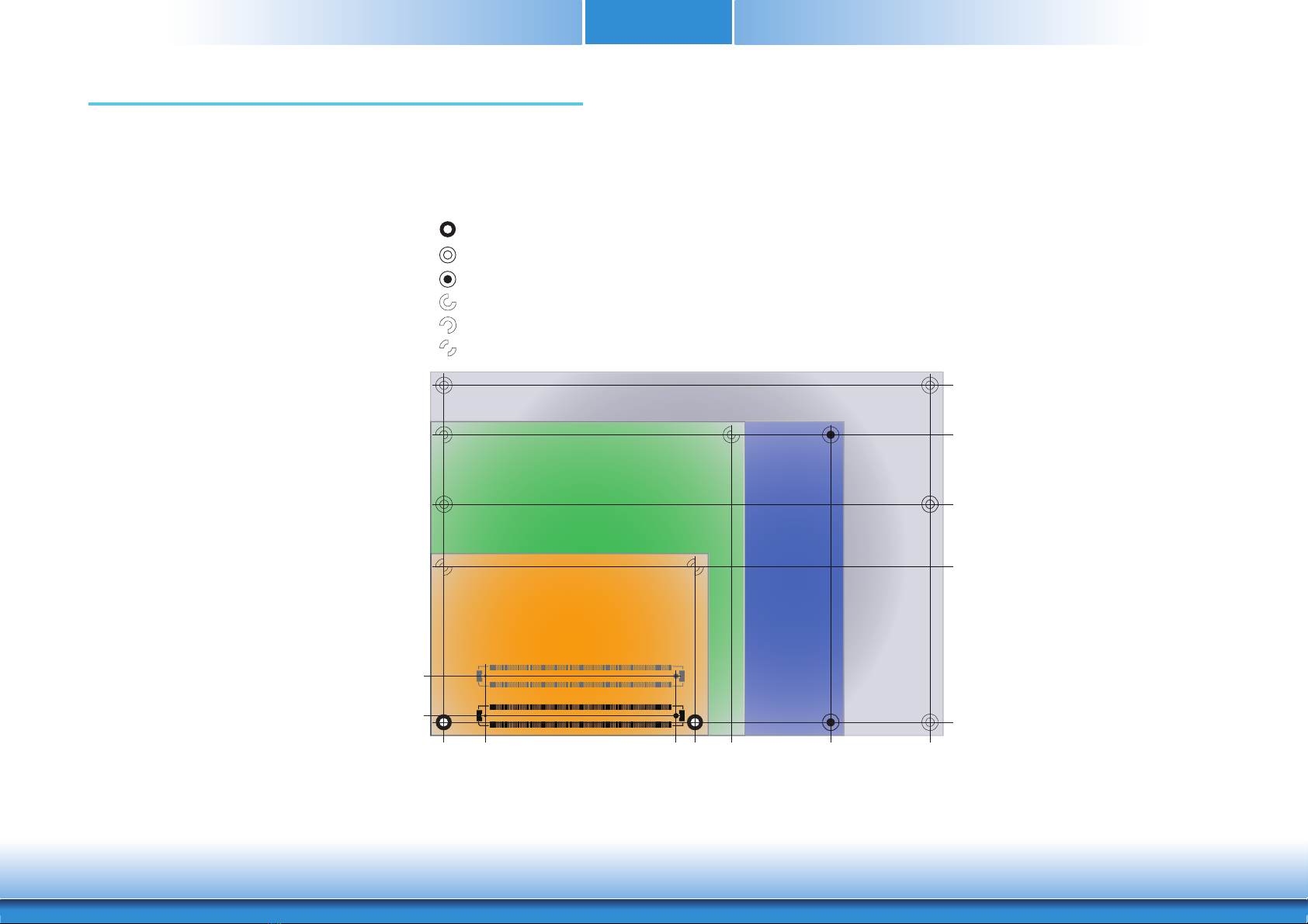
Mechanical Dimensions COM Express®Basic
95mm (3.74") x 125mm (4.9")
Compliance PICMG COM Express®R2.1, Type 6

www.dfi.comChapter 1 Introduction
7
Chapter 1
Features
• Watchdog Timer
The Watchdog Timer function allows your application to regularly “clear” the system at the set
time interval. If the system hangs or fails to function, it will reset at the set time interval so
that your system will continue to operate.
• DDR4
DDR4 delivers increased system bandwidth and improves performance. The advantages of
DDR4 provide an extended battery life and improve the performance at a lower power than
DDR3/DDR2.
• Graphics
The integrated Intel®HD graphics engine delivers an excellent blend of graphics performance
and features to meet business needs. It provides excellent video and 3D graphics with out-
standing graphics responsiveness. These enhancements deliver the performance and compat-
ibility needed for today’s and tomorrow’s business applications. Supports VGA, LVDS, eDP and
DDI display outputs.
• Serial ATA
The system supports multiple SATA 3.0 (up to 6Gb/s) ports and allows for different configura-
tions of RAID levels to meet various requirements for data redundancy and performance.
• Gigabit LAN
The Intel®I210IT Gigabit LAN controller features up to 1Gbps data transmission with support
for Intel®Active Management Technology. It provides remote maintenance and manageability
for networked computing assets in an enterprise environment.
• USB
The system board supports the new USB 3.0. It is capable of running at a maximum transmis-
sion speed of up to 5 Gbit/s (625 MB/s) and is faster than USB 2.0 (480 Mbit/s, or 60 MB/s)
and USB 1.1 (12Mb/s). USB 3.0 reduces the time required for data transmission, reduces
power consumption, and is backward compatible with USB 2.0. It is a marked improvement in
device transfer speeds between your computer and a wide range of simultaneously accessible
external Plug and Play peripherals.

www.dfi.comChapter 2 Concept
8
Chapter 2
Chapter 2 - Concept
COM Express Module Standards
The figure below shows the dimensions of the different types of COM Express modules.
SH960MD-CM236/QM170 is a COM Express Basic module. The dimension is 95mm x 125mm.
106.00
91.00
70.00
51.00
4.00
18.00
6.00
0.00
16.50
4.00
0.00
Extended
BasicCompact
Mini
74.20
80.00
91.00
121.00
151.00
Common for all Form Factors
Extended only
Basic only
Compact only
Compact and Basic only
Mini only

www.dfi.comChapter 2 Concept
9
Chapter 2
Specification Comparison Table
• 5 Indicates 12V-tolerant features on former VCC_12V signals.
• 6 Cells in the connected columns spanning rows provide a rough approximation of features
sharing connector pins.
The table below shows the COM Express standard specifications and the corresponding specifications supported on the SH960MD-CM236/QM170 module.
Connector Feature
COM Express Module Base Specification Type 6
(No IDE or PCI, add DDI+ USB3) Min / Max
DFI SH960MD
Type 6
A-B
A-B PCI Express Lanes 0 - 5 1 / 6 6
A-B LVDS Channel A 0 / 1 1
A-B LVDS Channel B 0 / 1 1
A-B eDP on LVDS CH A pins 0 / 1 1
A-B VGA Port 0 / 1 1
A-B TV-Out NA NA
A-B DDI 0 NA NA
A-B
5
Serial Ports 1 - 2 0 / 2 2
A-B CAN interface on SER1 0 / 1 0
A-B SATA / SAS Ports 1 / 4 4
A-B AC’97 / HDA Digital Interface 0 / 1 1
A-B USB 2.0 Ports 4 / 8 8
A-B USB Client 0 / 1 0
A-B USB 3.0 Ports NA NA
A-B LAN Port 0 1 / 1 1
A-B Express Card Support 1 / 2 2
A-B LPC Bus 1 / 1 1
A-B SPI 1 / 2 1
A-B
SDIO (muxed on GPIO) 0 / 1 NA
General Purpose I/O 8 / 8 8
A-B SMBus 1 / 1 1
A-B I2C 1 / 1 1
A-B Watchdog Timer 0 / 1 1
A-B Speaker Out 1 / 1 1
A-B External BIOS ROM Support 0 / 2 1
A-B Reset Functions 1 / 1 1
System I/O
System Management
A-B
6
Connector Feature
COM Express Module Base Specification Type 6
(No IDE or PCI, add DDI+ USB3) Min / Max
DFI SH960MD
Type 6
A-B
A-B Thermal Protection 0 / 1 1
A-B Battery Low Alarm 0 / 1 1
A-B Suspend/Wake Signals 0 / 3 2
A-B Power Button Support 1 / 1 1
A-B Power Good 1 / 1 1
A-B VCC_5V_SBY Contacts 4 / 4 4
A-B5Sleep Input 0 / 1 1
A-B5Lid Input 0 / 1 1
A-B5Fan Control Signals 0 / 2 1
A-B Trusted Platform Modules 0 / 1 1 (optional)
A-B
A-B VCC_12V Contacts 12 / 12 12
Power Management
Power
Module Pin-out - Required and Optional Features C-D Connector.
Connector Feature
COM Express Module Base Specification Type 6
(No IDE or PCI, add DDI+ USB3) Min / Max
DFI SH960MD
Type 6
C-D
PCI Express Lanes 16 - 31 0 / 16 16
PCI Express Graphics (PEG) 0 / 1 1
Muxed SDVO Channels 1 - 2 NA NA
PCI Express Lanes 6 - 7 0 / 2 2
PCI Bus - 32 Bit NA NA
PATA Port NA NA
LAN Ports 1 - 2 NA NA
DDIs 1 - 3 0 / 3 3 (DDI3 option)
USB 3.0 Ports 0 / 4 4
C-D
C-D VCC_12V Contacts 12 / 12 12
Power
System I/O
C-D6
C-D6
Module Pin-out - Required and Optional Features A-B Connector.

www.dfi.comChapter 3 Hardware Installation
10
Chapter 3
Chapter 3 - Hardware Installation
Board Layout
Top View
Bottom View
1
CPU Fan
Standby
Power
LED
Xeon/
Core/
Celeron
Intel
SPI Flash BIOS
Intel
CM236/QM170
SH960MD-CM236: CM236
SH960MD-QM170: QM170
Intel
I210IT
PTN3460
CH7517
DDR4
DDR4
DDR4
DDR4
DDR4
DDR4
DDR4
DDR4
DDR4
DDR4
DDR4
iTE
IT8528E
COM Express Connector
C110
D110
C1
D1
B110 B1
A110 A1
COM Express Connector
TPM
DDR4
DDR4
DDR4
DDR4
DDR4
DDR4
DDR4
DDR4
DDR4

Chapter 3 Hardware Installation
11
Chapter 3
DDR4
System Memory
Standby
Power LED
The system board is equipped with 8GB/16GB DDR4 onboard memory interfaces.
• Supports DDR4 2133MHz
• Supports dual channel memory interface
DDR4
Important:
Electrostatic discharge (ESD) can damage your board, processor, disk drives, add-in
boards, and other components. Perform installation procedures at an ESD workstation
only. If such a station is not available, you can provide some ESD protection by wear-
ing an antistatic wrist strap and attaching it to a metal part of the system chassis. If
a wrist strap is unavailable, establish and maintain contact with the system chassis
throughout any procedures requiring ESD protection.
Important:
When the Standby Power LED lit red, it indicates that there is power on the board.
Power-off the PC then unplug the power cord prior to installing any devices. Failure to
do so will cause severe damage to the board and components.
DDR4
DDR4

www.dfi.comChapter 3 Hardware Installation
12
Chapter 3
DDR4
Connectors
CPU Fan Connector
Connect the CPU fan’s cable connector to the CPU fan connector on the board. The cooling fan
will provide adequate airflow throughout the chassis to prevent overheating the CPU and board
components.
BIOS Setting
“PC Health Status” submenu in the Advanced menu of the BIOS will display the current speed
of the cooling fan. Refer to Chapter 4 for more information.
3
1
Sense
+12V
Ground
COM Express Connectors
The COM Express connectors are used to interface the SH960MD COMe board with a carrier
board. Connect the COM Express connectors (located on the solder side of the board) to the
COM Express connectors on the carrier board.
Refer to the “Installing COMe Board onto a Carrier Board” section for more information.
Refer to the following pages for the pin functions of these connectors.
COM Express Connectors
DDR4

www.dfi.comChapter 3 Hardware Installation
13
Chapter 3
- - - -
"+=4<-> "+=4<-> "+=4<-> "+=4<->
"8-JA "8-J5#K "+ "+
A "8-JAU 3J45-K 768J66< 768J66#<
H "8-J3+:K 3J5 768J66<U 768J66#<U
"8-J3+:K 3J5 "+ "+
E "8-J 3J5 768J66< 768J66#<
F "8-JU 3J5A 768J66<U 768J66#<U
"8-J3+:K 3JVK "+ "+
"8-J 3JVK 768J66< 768J66#<
"8-JU 3J3: 768J66<U 768J66#<U
"+=4<-> "+=4<-> "+=4<-> "+=4<->
"8-J 18#+K 768J66<A 768J66#<A
A "8-JU 68J: 768J66<AU 768J66#<AU
H "8-J#-4 68J5# "+ "+
676J6AK 68J53-#K J5EU J#33:J57<U
E 65#5J#<U 65#5J#<U J5E J#35#5J57<
F 65#5J#< 65#5J#< 69 69
676J6HK 676J6#5#K 69 69
65#5J<U 65#5J<U -J<EU -J#<EU
65#5J< 65#5J< -J<E -J#<E
"+=4<-> "+=4<-> "+=4<-> "+=4<->
65#5J#<U 65#5AJ#<U -J<FU -J#<FU
A 65#5J#< 65#5AJ#< -J<F -J#<F
H 676J6K 1J,: J2 69
65#5J<U 65#5AJ<U J5HU 69
E 65#5J< 65#5AJ< J5H J5U
F 85#3,1K 1# 69 J5
=6>5#5J5#K 5G25J6+ 69 69
5G25J6;+ 5G25J6+ J5U J5U
A 5G25J6#K 5G25J6+ J5 J5
A "+=4<-> "+=4<-> "+=4<-> "+=4<->
A 5G25J8#3: 6: J#33:J57<U J5U
AA 5G25J6,7# J: J#35#5J57< J5
AH 8,6J6K J5# JJ57<J6-3 JJ57<J6-3
A #2#K #2K 69 69
AE 768E 768F AJ#33:J57<U J5AU
AF 768EU 768FU AJ#35#5J57< J5A
A 768JEJFJ,K 768JHJJ,K AJJ57<J6-3 69
A 768H 768 AJ5U J5U
H 768HU 768U AJ5 J5
H "+=4<-> "+=4<-> "+=4<-> "+=4<->
COM Express Connectors
- - - -
H 768 768A AJ5U J5U
HA 768U 768AU AJ5 J5
HH 768JJAJ,K 768JJJ,K AJ2 J2
H 768 768 69 69
HE 768U 768U AJ5U J5U
HF 9J# -<J-6#K AJ5 J5
H -<J-6#K -<J-K 69 69
H -<J-K 6;6J-6-#K AJ5AU J5AU
3J6-V 8J-6-#K AJ5A J5A
"+=4<-> "+=4<-> "+=4<-> "+=4<->
-J#<U -J<U -"J<U -"J#<U
A -J#< -J< -"J< -"J#<
H " ", #;-K -"J35+-J9K
-J#<HU -J<HU -"J<U -"J#<U
E -J#<H -J<H -"J< -"J#<
F "+ ", #;-K #;-K
-J#<AU -J<AU -"J<U -"J#<U
-J#<A -J<A -"J< -"J#<
E "+=4<-> "+=4<-> "+=4<-> "+=4<->
E -J#<U -J<U -"J<AU -"J#<AU
E -J#< -J< -"J<A -"J#<A
EA " ",A 69 69
EH -J#<U -J<U 69 69
E -J#< -J< -"J<HU -"J#<HU
EE "+ 15:-K -"J<H -"J#<H
EF " 15:-K 69 "+
E -J#<U -J<U -"J<U -"J#<U
E -J#< -J< -"J< -"J#<
F "+=4<-> "+=4<-> "+=4<-> "+=4<->
F 396J5U 396J8U -"J<EU -"J#<EU
F 396J5 396J8 -"J<E -"J#<E
FA 396J5U 396J8U "+ "+
FH 396J5 396J8 -"J<FU -"J#<FU
F 396J5U 396J8U -"J<F -"J#<F
FE 396J5 396J8 "+ "+
FF 396J9J-+ 396J8AU 69 69
F 396J5AU 396J8A -"J<U -"J#<U
F 396J5A 396J8:3#J-+ -"J< -"J#<
"+=4<-> "+=4<-> "+=4<-> "+=4<->
396J5J:U 396J8J:U -"J<U -"J#<U
396J5J: 396J8J: -"J< -"J#<
A 396JJ: 396J8:3#J#3 69 69
H 396JJ5# 9J9J68; "+ "+
"A 9J9J68; -"J<U -"J#<U
E 69 9J9J68; -"J< -"J#<
F J2 9J9J68; "+ "+
-J3:J-4U 8,6J6K -"J<U -"J#<U
-J3:J-4 9"5J- -"J< -"J#<
"+=4<-> "+=4<-> "+=4<-> "+=4<->

www.dfi.comChapter 3 Hardware Installation
14
Chapter 3
- - - -
6J,1- 9"5J"+ -"J<U -"J#<U
6J6, 9"5J837 -"J< -"J#<
A ", 9"5J26;+ "+ "+
H 6J3: 9"5J96;+ -"J<AU -"J#<AU
6J,6 9"5JJ: -"J<A -"J#<A
E #J 9"5JJ5# "+ "+
F #;-K 6J6K 69 69
6-J#< 69 -"J<HU -"J#<HU
6-J< 69 -"J<H -"J#<H
"+=4<-> "+=4<-> "+=4<-> "+=4<->
6-J#<
45+J10,7#
-"J<U -"J#<U
6-J< 45+J#52+ -"J< -"J#<
A 3K 63--K "+ "+
H 9J9 9J9 9J9 9J9
9J9 9J9 9J9 9J9
E 9J9 9J9 9J9 9J9
F 9J9 9J9 9J9 9J9
9J9 9J9 9J9 9J9
9J9 9J9 9J9 9J9
"+=4<-> "+=4<-> "+=4<-> "+=4<->

www.dfi.comChapter 3 Hardware Installation
15
Chapter 3
COM Express Connectors Signal Description
Signal Pin# Pin Type Pwr Rail /Tolerance SH960MD PU/PD Module Base Specification R2.1 Description COM Express Carrier Design Guide R2.0 Description
HDA_RST# A30 O CMOS 3.3V Suspend/3.3V series 33ɏresistor Reset output to CODEC, active low. CODEC Reset.
HDA_SYNC A29 O CMOS 3.3V/3.3V series 33ɏresistor Sample-synchronization signal to the CODEC(s). Serial Sample Rate Synchronization.
HDA_BITCLK A32 I/O CMOS 3.3V/3.3V series 33ɏresistor Serial data clock generated by the external CODEC(s). 24 MHz Serial Bit Clock for HDA CODEC.
HDA_SDOUT A33 O CMOS 3.3V/3.3V series 33ɏresistor Serial TDM data output to the CODEC. Audio Serial Data Output Stream.
HDA_SDIN0 B30 I/O CMOS 3.3V Suspend/3.3V
HDA_SDIN1 B29 I/O CMOS 3.3V Suspend/3.3V
HDA_SDIN2 B28 I/O CMOS 3.3V Suspend/3.3V NC
Signal Pin# Pin Type Pwr Rail /Tolerance SH960MD PU/PD Module Base Specification R2.1 Description COM Express Carrier Design Guide R2.0 Description
GBE0_MDI0+ A13 I/O Analog 3.3V max Suspend
GBE0_MDI0- A12 I/O Analog 3.3V max Suspend
GBE0_MDI1+ A10 I/O Analog 3.3V max Suspend
GBE0_MDI1- A9 I/O Analog 3.3V max Suspend
GBE0_MDI2+ A7 I/O Analog 3.3V max Suspend
GBE0_MDI2- A6 I/O Analog 3.3V max Suspend
GBE0_MDI3+ A3 I/O Analog 3.3V max Suspend
GBE0_MDI3- A2 I/O Analog 3.3V max Suspend
GBE0_ACT# B2 OD CMOS 3.3V Suspend/3.3V Gigabit Ethernet Controller 0 activity indicator, active low. Ethernet controller 0 activity indicator, active low.
GBE0_LINK# A8 OD CMOS 3.3V Suspend/3.3V Gigabit Ethernet Controller 0 link indicator, active low. Ethernet controller 0 link indicator, active low.
GBE0_LINK100# A4 OD CMOS 3.3V Suspend/3.3V Gigabit Ethernet Controller 0 100 Mbit / sec link indicator, active low. Ethernet controller 0 100Mbit/sec link indicator, active low.
GBE0_LINK1000# A5 OD CMOS 3.3V Suspend/3.3V Gigabit Ethernet Controller 0 1000 Mbit / sec link indicator, active low. Ethernet controller 0 1000Mbit/sec link indicator, active low.
GBE0_CTREF A14 REF GND min 3.3V max NC
Reference volta
g
e for Carrier Board Ethernet channel 0 ma
g
netics
center
tap. The reference voltage is determined by the requirements of the
Module PHY and may be as low as 0V and as high as 3.3V.
The reference voltage output shall be current limited on the Module.
In
the case in which the reference is shorted to ground, the current shall
be
limited to 250 mA or less.
Reference voltage for Carrier Board Ethernet channel 0
magnetics center tap.
Pin Types
I Input to the Module
O Output from the Module
I/O Bi-directional input / output signal
OD Open drain output
RSVD pins are reserved for future use and should be no connect. Do not tie the RSVD pins together.
HDA Signals Descriptions
Serial TDM data inputs from up to 3 CODECs.
Gigabit Ethernet Signals Descriptions
Gigabit Ethernet Controller 0: Media Dependent Interface Differential
Pairs 0,1,2,3. The MDI can operate in 1000, 100 and 10 Mbit / sec
modes. Some pairs are unused in some modes, per the following:
1000BASE-T 100BASE-TX 10BASE-T
MDI[0]+/- B1_DA+/- TX+/- TX+/-
MDI[1]+/- B1_DB+/- RX+/- RX+/-
MDI[2]+/- B1_DC+/-
MDI[3]+/- B1_DD+/-
Audio Serial Data Input Stream from CODEC[0:2].
Media Dependent Interface (MDI) differential pair 0.
Media Dependent Interface (MDI) differential pair 1.
Media Dependent Interface (MDI) differential pair 2.
Only used for 1000Mbit/sec Gigabit Ethernet mode.
Media Dependent Interface (MDI) differential pair 3.
Only used for 1000Mbit/sec Gigabit Ethernet mode.

www.dfi.comChapter 3 Hardware Installation
16
Chapter 3
Signal Pin# Pin Type Pwr Rail /Tolerance SH960MD PU/PD Module Base Specification R2.1 Description COM Express Carrier Design Guide R2.0 Description
SATA0_TX+ A16 O SATA AC coupled on Module AC Coupling capacitor
SATA0_TX- A17 O SATA AC coupled on Module AC Coupling capacitor
SATA0_RX+ A19 I SATA AC coupled on Module AC Coupling capacitor
SATA0_RX- A20 I SATA AC coupled on Module AC Coupling capacitor
SATA1_TX+ B16 O SATA AC coupled on Module AC Coupling capacitor
SATA1_TX- B17 O SATA AC coupled on Module AC Coupling capacitor
SATA1_RX+ B19 I SATA AC coupled on Module AC Coupling capacitor
SATA1_RX- B20 I SATA AC coupled on Module AC Coupling capacitor
SATA2_TX+ A22 O SATA AC coupled on Module AC Coupling capacitor
SATA2_TX- A23 O SATA AC coupled on Module AC Coupling capacitor
SATA2_RX+ A25 I SATA AC coupled on Module AC Coupling capacitor
SATA2_RX- A26 I SATA AC coupled on Module AC Coupling capacitor
SATA3_TX+ B22 O SATA AC coupled on Module AC Coupling capacitor
SATA3_TX- B23 O SATA AC coupled on Module AC Coupling capacitor
SATA3_RX+ B25 I SATA AC coupled on Module AC Coupling capacitor
SATA3_RX- B26 I SATA AC coupled on Module AC Coupling capacitor
(S)ATA_ACT# A28 I/O CMOS 3.3V / 3.3V PU 10K:to 3.3V ATA (parallel and serial) or SAS activity indicator, active low. Serial ATA activity LED. Open collector output pin driven during
SATA command activity.
Signal Pin# Pin Type Pwr Rail /Tolerance SH960MD PU/PD Module Base Specification R2.1 Description COM Express Carrier Design Guide R2.0 Description
PCIE_TX0+ A68 AC Coupling capacitor
PCIE_TX0- A69 AC Coupling capacitor
PCIE_RX0+ B68
PCIE_RX0- B69
PCIE_TX1+ A64 AC Coupling capacitor
PCIE_TX1- A65 AC Coupling capacitor
PCIE_RX1+ B64
PCIE_RX1- B65
PCIE_TX2+ A61 AC Coupling capacitor
PCIE_TX2- A62 AC Coupling capacitor
PCIE_RX2+ B61
PCIE_RX2- B62
O PCIE AC coupled on Module PCI Express Differential Transmit Pairs 1
PCI Express Differential Receive Pairs 1
I PCIE AC coupled off Module PCI Express Differential Receive Pairs 2
PCIe channel 2. Transmit Output differential pair.
PCIe channel 2. Receive Input differential pair.
PCIe channel 1. Transmit Output differential pair.
PCIe channel 1. Receive Input differential pair.
Serial ATA channel 0
Transmit output differential pair.
Serial ATA channel 0
Receive input differential pair.
Serial ATA channel 1
Transmit output differential pair.
Serial ATA channel 3
Receive input differential pair.
O PCIE AC coupled on Module PCI Express Differential Transmit Pairs 0
O PCIE AC coupled on Module PCI Express Differential Transmit Pairs 2
I PCIE AC coupled off Module
I PCIE AC coupled off Module PCI Express Differential Receive Pairs 0
Serial ATA channel 2
Receive input differential pair.
Serial ATA channel 3
Transmit output differential pair.
PCIe channel 0. Transmit Output differential pair.
PCIe channel 0. Receive Input differential pair.
Serial ATA channel 2
Transmit output differential pair.
PCI Express Lanes Signals Descriptions
Serial ATA or SAS Channel 0 transmit differential pair.
Serial ATA or SAS Channel 0 receive differential pair.
Serial ATA or SAS Channel 3 transmit differential pair.
Serial ATA or SAS Channel 3 receive differential pair.
Serial ATA or SAS Channel 2 receive differential pair.
Serial ATA or SAS Channel 2 transmit differential pair.
Serial ATA or SAS Channel 1 receive differential pair.
SATA Signals Descriptions
Serial ATA or SAS Channel 1 transmit differential pair.
Serial ATA channel 1
Receive input differential pair.

www.dfi.comChapter 3 Hardware Installation
17
Chapter 3
Signal Pin# Pin Type Pwr Rail /Tolerance SH960MD PU/PD Module Base Specification R2.1 Description COM Express Carrier Design Guide R2.0 Description
PCI Express Lanes Signals Descriptions
PCIE_TX3+ A58 AC Coupling capacitor
PCIE_TX3- A59 AC Coupling capacitor
PCIE_RX3+ B58
PCIE_RX3- B59
PCIE_TX4+ A55 AC Coupling capacitor
PCIE_TX4- A56 AC Coupling capacitor
PCIE_RX4+ B55
PCIE_RX4- B56
PCIE_TX5+ A52 AC Coupling capacitor
PCIE_TX5- A53 AC Coupling capacitor
PCIE_RX5+ B52
PCIE_RX5- B53
PCIE_TX6+ D19 AC Coupling capacitor
PCIE_TX6- D20 AC Coupling capacitor
PCIE_RX6+ C19
PCIE_RX6- C20
PCIE_TX7+ D22 AC Coupling capacitor
PCIE_TX7- D23 AC Coupling capacitor
PCIE_RX7+ C22
PCIE_RX7- C23
PCIE_CLK_REF+ A88
PCIE_CLK_REF- A89
Signal Pin# Pin Type Pwr Rail /Tolerance SH960MD PU/PD Module Base Specification R2.1 Description COM Express Carrier Design Guide R2.0 Description
PEG_TX0+ D52 AC Coupling capacitor
PEG_TX0- D53 AC Coupling capacitor
PEG_RX0+ C52
PEG_RX0- C53
PCIe channel 4. Receive Input differential pair.
PCIe channel 5. Transmit Output differential pair.
PCIe channel 6. Transmit Output differential pair.
PCIe channel 6. Receive Input differential pair.
PCIe channel 7. Transmit Output differential pair.
PCIe channel 7. Receive Input differential pair.
PCIe Reference Clock for all COM Express PCIe lanes, and for
PEG lanes.
PEG Signals Descriptions
O PCIE AC coupled on Module PCI Express Graphics transmit differential pairs 0
I PCIE AC coupled off Module PCI Express Graphics receive differential pairs 0
PEG channel 0, Transmit Output differential pair.
PEG channel 0, Receive Input differential pair.
PCI Express Differential Receive Pairs 7
O PCIE PCIE Reference clock output for all PCI Express and PCI Express Graphics
lanes.
PCI Express Differential Receive Pairs 6
O PCIE AC coupled on Module PCI Express Differential Transmit Pairs 7
PCI Express Differential Transmit Pairs 4
PCIe channel 5. Receive Input differential pair.
PCIe channel 4. Transmit Output differential pair.
I PCIE AC coupled off Module
O PCIE AC coupled on Module PCI Express Differential Transmit Pairs 6
I PCIE AC coupled off Module PCI Express Differential Receive Pairs 5
O PCIE AC coupled on Module PCI Express Differential Transmit Pairs 5
PCI Express Differential Receive Pairs 4
O PCIE AC coupled on Module
I PCIE AC coupled off Module
PCIe channel 3. Receive Input differential pair.PCI Express Differential Receive Pairs 3
PCI Express Differential Transmit Pairs 3O PCIE AC coupled on Module PCIe channel 3. Transmit Output differential pair.
I PCIE AC coupled off Module

www.dfi.comChapter 3 Hardware Installation
18
Chapter 3
Signal Pin# Pin Type Pwr Rail /Tolerance SH960MD PU/PD Module Base Specification R2.1 Description COM Express Carrier Design Guide R2.0 Description
PEG Signals Descriptions
PEG_TX1+ D55 AC Coupling capacitor
PEG_TX1- D56 AC Coupling capacitor
PEG_RX1+ C55
PEG_RX1- C56
PEG_TX2+ D58 AC Coupling capacitor
PEG_TX2- D59 AC Coupling capacitor
PEG_RX2+ C58
PEG_RX2- C59
PEG_TX3+ D61 AC Coupling capacitor
PEG_TX3- D62 AC Coupling capacitor
PEG_RX3+ C61
PEG_RX3- C62
PEG_TX4+ D65 AC Coupling capacitor
PEG_TX4- D66 AC Coupling capacitor
PEG_RX4+ C65
PEG_RX4- C66
PEG_TX5+ D68 AC Coupling capacitor
PEG_TX5- D69 AC Coupling capacitor
PEG_RX5+ C68
PEG_RX5- C69
PEG_TX6+ D71 AC Coupling capacitor
PEG_TX6- D72 AC Coupling capacitor
PEG_RX6+ C71
PEG_RX6- C72
PEG_TX7+ D74 AC Coupling capacitor
PEG_TX7- D75 AC Coupling capacitor
PEG_RX7+ C74
PEG_RX7- C75
PEG_TX8+ D78 AC Coupling capacitor
PEG_TX8- D79 AC Coupling capacitor
PEG_RX8+ C78
PEG_RX8- C79
O PCIE
O PCIE AC coupled on Module PCI Express Graphics transmit differential pairs 6
PEG channel 5, Receive Input differential pair.
PEG channel 6, Transmit Output differential pair.
PEG channel 6, Receive Input differential pair.
PEG channel 7, Transmit Output differential pair.
PEG channel 7, Receive Input differential pair.
PEG channel 8, Transmit Output differential pair.O PCIE AC coupled on Module
PCI Express Graphics receive differential pairs 8
I PCIE AC coupled off Module PCI Express Graphics receive differential pairs 7
AC coupled on Module PCI Express Graphics transmit differential pairs 7
I PCIE AC coupled off Module PCI Express Graphics receive differential pairs 6
PEG channel 8, Receive Input differential pair.I PCIE AC coupled off Module
PCI Express Graphics transmit differential pairs 8
I PCIE AC coupled off Module PCI Express Graphics receive differential pairs 5
PEG channel 5, Transmit Output differential pair.O PCIE AC coupled on Module
PCI Express Graphics transmit differential pairs 4
I PCIE AC coupled off Module
I PCIE AC coupled off Module PCI Express Graphics receive differential pairs 3
PCI Express Graphics transmit differential pairs 5
I PCIE AC coupled off Module PCI Express Graphics receive differential pairs 2
O PCIE AC coupled on Module PCI Express Graphics transmit differential pairs 3
PCI Express Graphics receive differential pairs 4
O PCIE AC coupled on Module
PEG channel 2, Receive Input differential pair.
PEG channel 3, Transmit Output differential pair.
PEG channel 3, Receive Input differential pair.
PEG channel 4, Transmit Output differential pair.
PEG channel 4, Receive Input differential pair.
PCI Express Graphics transmit differential pairs 2
O PCIE AC coupled on Module PCI Express Graphics transmit differential pairs 1
AC coupled off Module PCI Express Graphics receive differential pairs 1
PEG channel 1, Transmit Output differential pair.
PEG channel 1, Receive Input differential pair.
PEG channel 2, Transmit Output differential pair.O PCIE AC coupled on Module
I PCIE

www.dfi.comChapter 3 Hardware Installation
19
Chapter 3
Signal Pin# Pin Type Pwr Rail /Tolerance SH960MD PU/PD Module Base Specification R2.1 Description COM Express Carrier Design Guide R2.0 Description
PEG Signals Descriptions
PEG_TX9+ D81 AC Coupling capacitor
PEG_TX9- D82 AC Coupling capacitor
PEG_RX9+ C81
PEG_RX9- C82
PEG_TX10+ D85 AC Coupling capacitor
PEG_TX10- D86 AC Coupling capacitor
PEG_RX10+ C85
PEG_RX10- C86
PEG_TX11+ D88 AC Coupling capacitor
PEG_TX11- D89 AC Coupling capacitor
PEG_RX11+ C88
PEG_RX11- C89
PEG_TX12+ D91 AC Coupling capacitor
PEG_TX12- D92 AC Coupling capacitor
PEG_RX12+ C91
PEG_RX12- C92
PEG_TX13+ D94 AC Coupling capacitor
PEG_TX13- D95 AC Coupling capacitor
PEG_RX13+ C94
PEG_RX13- C95
PEG_TX14+ D98 AC Coupling capacitor
PEG_TX14- D99 AC Coupling capacitor
PEG_RX14+ C98
PEG_RX14- C99
PEG_TX15+ D101 AC Coupling capacitor
PEG_TX15- D102 AC Coupling capacitor
PEG_RX15+ C101
PEG_RX15- C102
PEG_LANE_RV# D54 I CMOS 3.3V / 3.3V PU 10Kɏto 3V3 PCI Express Graphics lane reversal input strap.
Pull low on the Carrier board to reverse lane order.
PCI Express Graphics lane reversal input strap.
Pull low on the carrier board to reverse lane order.
I PCIE
PEG channel 15, Transmit Output differential pair.
PCI Express Graphics transmit differential pairs 12
O PCIE AC coupled on Module PCI Express Graphics transmit differential pairs 11
PEG channel 15, Receive Input differential pair.
I PCIE AC coupled off Module
O PCIE AC coupled on Module
I PCIE AC coupled off Module
PCI Express Graphics receive differential pairs 14
PCI Express Graphics receive differential pairs 12
O PCIE AC coupled on Module PCI Express Graphics transmit differential pairs 14
I PCIE AC coupled off Module PCI Express Graphics receive differential pairs 15
PEG channel 12, Receive Input differential pair.
PEG channel 13 Transmit Output differential pair.
PEG channel 13, Receive Input differential pair.
PEG channel 14, Transmit Output differential pair.
PEG channel 14, Receive Input differential pair.
PEG channel 9, Transmit Output differential pair.
PEG channel 9, Receive Input differential pair.
PEG channel 10, Transmit Output differential pair.O PCIE AC coupled on Module
PCI Express Graphics receive differential pairs 13
O PCIE AC coupled on Module PCI Express Graphics transmit differential pairs 15
I PCIE AC coupled off Module
O PCIE AC coupled on Module PCI Express Graphics transmit differential pairs 13
AC coupled off Module
I PCIE AC coupled off Module PCI Express Graphics receive differential pairs 11
PCI Express Graphics receive differential pairs 10 PEG channel 10, Receive Input differential pair.
PEG channel 11, Transmit Output differential pair.
PEG channel 11, Receive Input differential pair.
PEG channel 12, Transmit Output differential pair.
PCI Express Graphics transmit differential pairs 10
I PCIE AC coupled off Module PCI Express Graphics receive differential pairs 9
O PCIE AC coupled on Module PCI Express Graphics transmit differential pairs 9

www.dfi.comChapter 3 Hardware Installation
20
Chapter 3
Signal Pin# Pin Type Pwr Rail /Tolerance SH960MD PU/PD Module Base Specification R2.1 Description COM Express Carrier Design Guide R2.0 Description
EXCD0_CPPE# A49 I CMOS 3.3V /3.3V PU 10k to 3.3V PCI ExpressCard: PCI Express capable card request, active low, one
per card
PCI ExpressCard0: PCI Express capable card request, active low,
one per card
EXCD0_PERST# A48 O CMOS 3.3V /3.3V PCI ExpressCard: reset, active low, one per card PCI ExpressCard0: reset, active low, one per card
EXCD1_CPPE# B48 I CMOS 3.3V /3.3V PU 10k to 3.3V PCI ExpressCard: PCI Express capable card request, active low, one
percard
PCI ExpressCard1: PCI Express capable card request, active low,
one per card
EXCD1_PERST# B47 O CMOS 3.3V /3.3V PCI ExpressCard: reset, active low, one per card PCI ExpressCard1: reset, active low, one per card
Signal Pin# Pin Type Pwr Rail /Tolerance SH960MD PU/PD Module Base Specification R2.1 Description COM Express Carrier Design Guide R2.0 Description
USB0+ A46 USB Port 0, data + or D+
USB0- A45 USB Port 0, data - or D-
USB1+ B46 USB Port 1, data + or D+
USB1- B45 USB Port 1, data - or D-
USB2+ A43 USB Port 2, data + or D+
USB2- A42 USB Port 2, data - or D-
USB3+ B43 USB Port 3, data + or D+
USB3- B42 USB Port 3, data - or D-
USB4+ A40 USB Port 4, data + or D+
USB4- A39 USB Port 4, data - or D-
USB5+ B40 USB Port 5, data + or D+
USB5- B39 USB Port 5, data - or D-
USB6+ A37 USB Port 6, data + or D+
USB6- A36 USB Port 6, data - or D-
USB7+ B37 USB Port 7, data + or D+
USB7- B36 USB Port 7, data - or D-
USB_0_1_OC# B44 I CMOS 3.3V Suspend/3.3V PU 10K:to 3.3V
Suspend
USB over-current sense, USB channels 0 and 1. A pull-up for this line
shall be present on the Module. An open drain driver from a USB
current monitor on the Carrier Board may drive this line low. Do not
pull this line high on the Carrier Board.
USB over-current sense, USB ports 0 and 1.
USB_2_3_OC# A44 I CMOS 3.3V Suspend/3.3V PU 10K:to 3.3V
Suspend
USB over-current sense, USB channels 2 and 3. A pull-up for this line
shall be present on the Module. An open drain driver from a USB
current monitor on the Carrier Board may drive this line low. Do not
pull this line high on the Carrier Board.
USB over-current sense, USB ports 2 and 3.
USB_4_5_OC# B38 I CMOS 3.3V Suspend/3.3V PU 10K:to 3.3V
Suspend
USB over-current sense, USB channels 4 and 5. A pull-up for this line
shall be present on the Module. An open drain driver from a USB
current monitor on the Carrier Board may drive this line low. Do not
pull this line high on the Carrier Board.
USB over-current sense, USB ports 4 and 5.
ExpressCard Signals Descriptions
I/O USB 3.3V Suspend/3.3V USB differential pairs, channel 2
I/O USB
I/O USB 3.3V Suspend/3.3V USB differential pairs, channel 6
3.3V Suspend/3.3V USB differential pairs, channel 5
I/O USB 3.3V Suspend/3.3V
USB differential pairs, channel 7.
USB7 may be configured as a USB client or as a host, or both, at the
Module designer's discretion. (SH960MD default set as a host)
3.3V Suspend/3.3V USB differential pairs, channel 4
I/O USB 3.3V Suspend/3.3V USB differential pairs, channel 3
I/O USB
3.3V Suspend/3.3V USB differential pairs, channel 1
USB Signals Descriptions
I/O USB 3.3V Suspend/3.3V USB differential pairs, channel 0
I/O USB
Table of contents
Other DFI Control Unit manuals