Dinamap 7300 User manual

NIBP SINGLEWIDE MODULE
INTRODUCTION
This area contains component information about the
singlewide Model 7300 Non-Invasive Blood
Pressure (NIBP) Module. The singlewide NIBP
module monitors blood pressure noninvasively,
using the oscillometric method that measures the
amplitude of the pressure oscillations within the
blood pressure cuff. Systolic pressure, diastolic
pressure, mean arterial pressure, and cuff pressure
are all measured by the module. Heart rate values
are also derived from the pulse rate determined by
the oscillometric blood pressure measurement
technique.

PHYSICAL
DESCRIPTION
The singlewide version of the NIBP module, shown
in FO-42B, occupies a single module slot. The
module consists of two PWAs, interconnect cabling,
a pump manifold assembly, a cuff manifold
assembly, and a mechanical enclosure. Digital
PWA 315459 includes an interface to the PNet
communication bus, module core logic, and the
analog to digital conversion subsystem.
Analog PWA 315452 includes the pressure
transducer amplifiers and filter circuitry, pneumatic
system overpressure detection circuit, and the
pneumatic valves and pump control. The digital
PWA, with its PNet connector, occupies the left slot in
the module enclosure when viewed from the sensor
connector end (front) of the module. The analog
PWA occupies the right slot in the module enclosure.
Flex cable W100 connects the digital and analog
PWAs. It is soldered to the analog PWA, and
attaches to a pin header on the digital PWA. Flex
PWA 313-113 connects the analog PWA to
transducer XD2, mounted on the cuff manifold
assembly. Flex PWA 313-114 connects the analog
PWA to transducer XD1, mounted on the pump
manifold assembly. Cable assembly W102
connects the analog PWA to the pump, zero/deflate
valve, and dump valve mounted on the pump
manifold assembly.

FUNCTIONAL
PRINCIPLES OF
OPERATION
A schematic diagram of the pneumatics system is
shown in Figure 4-1. It illustrates all connections to
valves, transducers, and pump. The pump draws air
in and forces it through the check valve to the system
manifold. The filtered orifice is used to bleed off air
in the chamber between the pump and check valve.
This allows the pump to start up without back
pressure. The check valve prevents pressurized air
in the system from going back through the pump
when it shuts off. Transducer XD2 monitors the total
system pressure and provides an overpressure
signal to the analog PWA when the pressure gets
too high. During an overpressure condition,
deflate/zero valve V2 energizes and vents the
pressurized air to the atmosphere. Transducer XD1
monitors pressure through the cuff during a blood
pressure measurement. After the blood pressure
measurement is complete (or after power failure),
dump valve V3 deenergizes and vents the
pressurized cuff to the atmosphere.
A functional block diagram of the NIBP Singlewide
Module is shown in FO-42A. The diagram is divided
into analog circuits and core logic circuits. The
analog circuits are shown in the top half of sheets 1
and 2 and the core logic circuits are shown in the
bottom half of sheets 1 and 2.

Figure 4-1. NIBP Singlewide Pneumatics Schematic

Analog Circuits
The analog circuits consist of cuff measurement,
overpressure, and pneumatics circuits.
Transducers XD1 and XD2 shown on sheet 1
receive excitation voltage from +10V references.
Differential signal XD1SIG+/- from transducer XD1
representing blood pressure is applied to the analog
multiplexer through the pre-amp and low pass filter.
The pre-amp is gain controlled and the filter
removes any erratic and false data from the signal.
Differential signal XD2SIG+/- representing system
pressure from transducer XD2 is applied to the
overpressure amplifier. Overpressure threshold is
programmed by the CPU to a specific level. This
threshold level and the actual system pressure are
summed together by the summing amplifier and
applied to the delay circuit. This built-in delay
prevents a false overpressure caused by transient
surges in the system pressure. The overpressure
threshold control also allows selection of either
neonatal or adult pressure limits via ADULT-0
signal. This signal is true when an adult cuff is
attached, and false when a neonatal cuff is attached.
The CPU addresses the analog multiplexer through
ASEL0 through ASEL2. This allows the multiplexer
to poll any of seven inputs (AIN1 through AIN7).
Thus, the multiplexer monitors transducer
references and outputs, system pressure and
overpressure, and pump drive outputs. This
multiplexed analog signal (BUF_ANA_MUX) is
converted to digital by the A/D converter and sent to
the CPU for evaluation and response.
The pneumatics decode logic circuits shown on
sheet 2 provide a logical sequence of inflation after
receiving a RESET-0 signal. CLAMP1 and CLAMP2
signals control the transducer gain circuits shown
on sheet 1. ADULT-0 signal is generated when an
adult cuff is attached, and provides higher
overpressure limits. This logic also controls the
pneumatics latch and solenoid drive circuits.

The pneumatics latch and solenoid drive circuits
control the pump drive and the dump and
deflate/zero valves. Pneumatic reset or failsafe
signals from the CPU shut down the pump and open
the dump valve. Signal PUMPC measures pump
current. This allows the CPU to monitor when the
pump is running. DEFLATE_VAL signal from the
pneumatics latch and solenoid drive circuit
energizes deflate valve V2, releasing cuff pressure.
DUMP_VAL signal deenergizes dump valve V3,
releasing all system pressure. Both valves receive
+12V power from the analog PWA.
Core Logic Circuits
The core logic circuits are shown on sheet 2 of
FO-42A. Functional blocks include the PNet
interface, reset/failsafe, 68302 CPU, 128Kx8 data
memory, 128Kx8 program memory, the model and
serial number EEPROM, and logic analyzer/test
interface.
The Module will not be damaged when plugged into
a live slot. Core logic power inputs to a Module are
limited to a peak inrush current during hot-plugging.
Within 2 seconds the Module will respond to
identification and wake up in a minimized power
state until registered with the system.
The PNet interface allows asynchronous and
synchronous data transfer between the core logic
and the external devices. Synchronous operation is
always used in MPS systems. Asynchronous
operation is for test and development only. The
reset/failsafe logic provides power-on reset,
processor reset and halt, and failsafe if a problem
occurs with the microprocessor. The
microprocessor controls and transfers data within
the core logic. The program memory is a FLASH
device that can be loaded with program information
from the PNET interface or the logic analyzer
interface. Data memory temporarily stores status
and monitoring data for processing.

COMPONENT
PRINCIPLES OF
OPERATION
The following paragraphs describe the function of
the two rigid PWAs. The NIBP analog PWA provides
the circuitry for the excitation, amplification, and
signal conditioning (filtering) for measurement of
non-invasive blood pressure within the NIBP
module. Also included are the associated circuitry
for a separate, independent direct overpressure
interactive channel. The NIBP digital PWA provides
the processor, communication, and analog to digital
conversion for the NIBP module. Schematic
diagrams SC315-452 and SC315-459 are provided.
The mapping of signals located in the CPU Port
Register A and Port Register B are listed in Table
42-1.
Table 42-1. CPU Register Mapping
Mapping of Bits in Port A:
Bit Signal Type Comment
PA(0) SCC2 RXD input debug serial data to
PA(1) SCC2 TXD output debug: serial data from
PA(2) SP_CS output Enable for Serial EEPROM
PA(3) Failsafe-1 input Monitor status of Failsafe latch
PA(4) PNEURESET output Pulsed low-high-low to reset
PA(5) ASYNC-EN output Selects Com Mode for PNET, H=Async
PA(6) MOTOR_PWR_CNTL output Delayed Power to Motor & Valves
PA(7) LATCHED_OVC input Latched Over_Current, normal=1
PA(8) DATA FROM ISO input (Unused)
PA(9) DATA TO ISO output (Unused)
PA(10) SPARE 1
PA(11) ADCLK output SCC3 (TxCLK)
PA(12) UFIL_OVP-0 input Unfiltered Overpressure (OVP-0)
PA(13) ASEL0 output Analog Mux -LSB
PA(14) ASEL1 output Analog Mux
PA(15) ASEL2 output Analog Mux -MSB

Table 42-1. CPU Register Mapping (Continued)
Mapping of Bits in Port B:
Bit Signal Type Comment
PB(0) LATCH_OVP input Latched Overpressure, normal =1
PB(1) POTCS-0 output init_val =1
PB(2) POTINC-0 output init_val = 1
PB(3) POTU~D-0 output init_val = 0
PB(4) TOUT1-0 output (Not used)
PB(5) TIN2 input **Debug Only
PB(6) PT1_CLAMP-0 output init_val = 1
PB(7) WDOG-0 output WatchDog Timer, normal =1
PB(8) FPTTST-0 output init_val = 1
PB(9) ADCBUSY-0 input busy = 0
PB(10) SYNC-0 input PNet
PB(11) SELECT-0 input PNet

Analog PWA
The NIBP analog PWA includes four functional
circuits: analog mux, filtered NIBP, overpressure,
and pneumatics.
Analog Mux
The analog mux functional block consists of a single
eight-to-one analog multliplexer and includes an
output buffer amplifer. Data is transferred to the
digital card via a single analog channel
BUF_ANA_MUX (MUX_OUT) on J100, Pin2. Channel
selection is defined by three address lines
ASEL0-ASEL2 in connector J100. These channel
assignments are defined in Table 42-2.
Table 42-2. Analog Multiplexer Channel Assignments
Channel ASEL0 ASEL1 ASEL2 Signal Description
AIN0 0 0 0 MOTRC_REF Motor Current Limit Ref Voltage
AIN1 1 0 0 TH_VREF Overpressure Threshold
Voltage
AIN2 0 1 0 PT2 Unfiltered Manifold Pressure
AIN3 1 1 0 PT2_REF XDCR2 Excitation Voltage Ref
AIN4 0 0 1 FPT1 Filter Cuff Pressure
AIN5 1 0 1 PT1 Unfiltered Cuff Pressure
AIN6 0 1 1 PT1_REF XDCR1 Excitation Voltage Ref
AIN7 1 1 1 PUMPC Pump Current Sense Voltage

Filtered NIBP
The filtered NIBP functional block consists of signal
conditional circuitry required to measure the cuff
oscillatory pressure (PT1) and acquire a blood
pressure determination. Circuitry for offset, voltage
clamping, and test pulse injection are also included.
The excitation voltage for the cuff transducer is
derived from the analog-to-digital converter, located
on the digital PWA. Changes in the A/D derived
reference produce a ratiometric change in the
channel and tend to compensate for the initial
reference change.
A +350mV nominal offset is added to the PT1
channel to insure its signal remains positive, since
the A/D converter input signal is limited to a uni-
polar, 0 to 5.0 Volts range. The FPT1 channel has a
+200mV nominal offset.
The pulse component (typically one percent) of the
cuff pressure signal is separated from the cuff
pressure signal by a cascaded high-pass filter
section followed by a low-pass filter section. Each
filter section contains two poles. The passband of
this filter is nominally 0.5 to 7.2 Hz. Testing of filter
characteristics is accomplished using the FSTTST
signal.

The blood pressure algorithm requires the ability to
initialize (clamp) the high pass filter in the process of
separating and measuring the pulse signal. Two
clamps are used in this process. FLT_Clamp-0
provides a clamp to ground of the input to the
second stage and also clamps the output buffer to a
+200 mV offset reference voltage. The second
clamp, PT1_Clamp-0 is used to isolate the input
channel to zero. This clamp is applied to disconnect
the input pressure transducer signal from the
channel. This permits a true, uncorrupted test signal
to be injected in to the input of the channel to
measure filter characteristics. This test pulse is
accomplished by toggling the FPTTST-0 signal.
FPTTST-0 should normally be held HIGH, otherwise
it will inject a nominal offset of 37.5 mV in the PT1
channel.
The inputs to both pressure measurement channels
PT1 and PT2 are derived from a pressure transducer
having the characteristics defined in Table 42-3.
Table 42-4 defines the range of parameter variations
for the cuff measurement channel.
Table 42-3. Transducer Characteristics
Operating Conditions: Excitation voltage = +10.000V
Characteristics Symbol Min Typ Max Units
Pressure Range P 0 375 mmHg
XDCR,FSS VFSS 38.5 40 41.5 mV
XDCR, OFFSET VFSS -1.0 +1.0 mV
Linearity, of XDCR -0.25 +0.25 %FSS
FSS == Full Scale Span
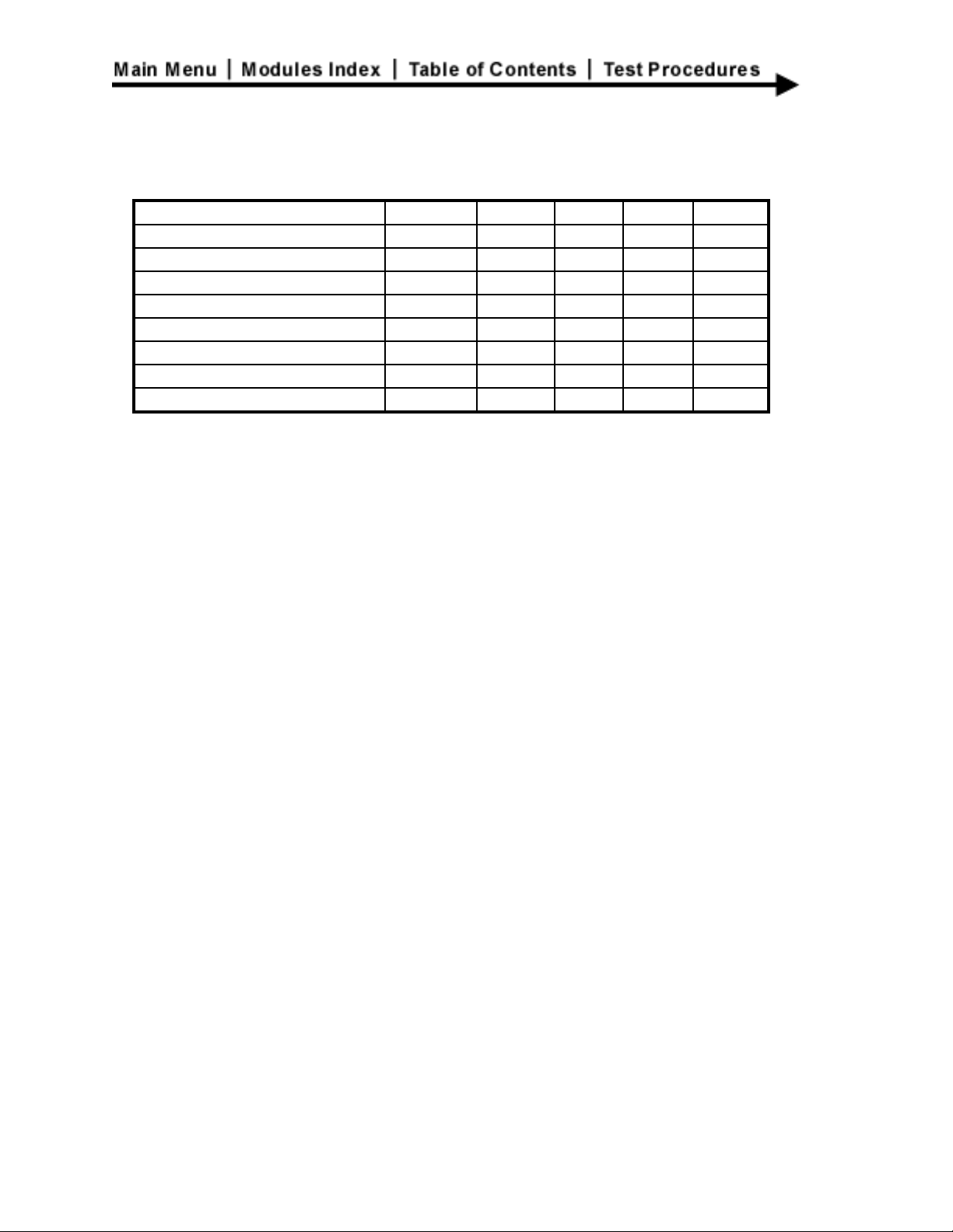
Table 42-4. PT1 Output Characteristics
Operating Conditions: Power Supply Voltages=+5V+/-5%, +12V+/-5%, -12V+/-5%
Characteristics Symbol Min Typ Max Units
Gain* G2 88.83 91.89 94.96
Offset Voff 335 349 363 mV
Offset, including AD2 ref Voff 326 349 372 mV
XDCR,FSS VFSS 38.5 40 41.5 mV
XDCR, OFFSET VFSS -1.0 +1.0 mV
Linearity, with XDCR -0.25 +0.25 %FSS
Full Scale Scan, with XDCR VFSS 3511 3676 3842 mV
Offset Voltage, with XDCR Voff 178 349 495 mV
*Gain of signal [range 1-40mv] injected between pins J103-Pin4 and J103-Pin2
Overpressure
The overpressure circuit generates a separate,
independent pressure measurement channel (PT2),
including its own separate excitation voltage source
(Table 42-5). Also included is circuitry for
electronically setting the overpressure threshold
point. Both the excitation reference voltage PT2_REF
and the unfiltered pressure transducer (PT2), which
is amplified and buffered, are available as output to
the A/D converter. The PT2 channel also has a +350
mV offset voltage injected to insure the uni-polar A/D
converter input always remains positive (Table 42-6).

Table 42-5. PT2 Output Characteristics
Operating Conditions: Power Supply Voltages = +5V+/-5%, +12V+/-5%, -12V+/-5%
Characteristics Symbol Min Typ Max Units
Gain* G2 90.70 91.89 93.08
Offset Voff 339 349 359 mV
Linearity, with XDCR -0.25 +0.25 %FSS
Full Scale Scan, with XDCR VFSS 3555 3676 3904 mV
Offset Voltage, with XDCR Voff 178 349 495 mV
*Gain of signal [range 1-40mv] injected between pins J103-Pin3 and J103-Pin5
Table 42-6. Reference Output Characteristics
Operating Conditions: Power Supply Voltages = +5V+/-5%, +12V+/-5%, -12V+/-5%
Characteristics Symbol Min Typ Max Units
PT1 Reference Voltage PT2_REF 3253 3329 3406 mV
PT2 Reference Voltage PT2_REF 3253 3329 3406 mV
FPT1 Reference Voltage FPT1 170 200 230 mV
OverPressure Threshold Voltage
Adult Mode
Neonate Mode
TH_VREF
2952
1364
3290
1530
3700
2047
mV
mV
Motor Over Current Ref Voltage MOTR_C_Ref 2424 2500 2574 mV
PT1 EXCITATION Voltage EXC1+ 10.000 V
PT2 EXCITATION Voltage EXC2+ 10.000 V
The excititation reference voltage for transducer PT2
is used to generate a threshold voltage to compare
with the actual pressure of the cuff as measured by
transducer PT2. The reference voltage is buffered by
an adjustable gain amplifier to produce the
reference pressure point of 300 mmHg (150 mmHg
in neonate mode) for the trip point. The amplifier
gain is altered by modifing the feedback resistance
of the amplifier by means of a solid state non-
volatile, digital E2POT. The digital E2POT has a
resolution of 100 steps. Total adjustment trim range
is limited to about +/-10%.

Threshold trimming is accomplished by controlling
three input signals: CS-0 (Chip Select), U_D-0
(Direction: Up or Down), and INC-0 (Increment or
Decrement). A interlock jumper, JP1, which
connects CS-0 to the board edge pin, is required to
be installed or threshold adjustment is inhibited.
The E2POT incorporates a storage mode that
permits maintaining the threshold setting once
adjusted. The last state saved is recalled from non-
volatile storage on system power-on, returning the
overpressure threshold point to the previous set
point.
Pneumatics
The pneumatic functional block includes the control
signal decode logic, the valve driver circuitry, the
pump driver circuitry, pump current measurement
circuit, and a safety interlock circuit.
Control signals for the board are derived via three
different sources: direct control from registered
outputs of the processor, controls signal derived
from processor address write commands (which are
stored in an addressable latch), signals derived
from the watchdog timer, and signals generated by
the overpressure functional block. The four valve
control signals and the pump control signal are
derived from the write address and stored in an
addressable latch. The latch signals are defined in
Table 42-7. Latch values are cleared by application
of system RESET generated by the processor. Refer
to Table 42-8 for reset conditions. Each latch signal
is individually gated in a programmable logic device
(22v10) with the fail safe input signal (watchdog
timer) and the overpressure latch output to ensure
pressure is removed from the patient cuff should
either overpressure or processor hang-up condition
occur.

Table 42-7. Latched Control Signals and Decode Matrix
Operating Conditions: RESET-0 =1; PNEURESET=1; FAILSAFE-0 =1; FLT_0VP-0=1
Pneu_Enab Data LSEL0 LSEL1 LSEL2 Signal Value Description
¥ 0
1
000TK_Inflate_Val Open
Closed
Not Used
¥ 0
1
000Cuff_Deflate_Val Closed
Open
When open, deflates Cuff
¥ 0
1
100Cuff_Dump_Val Open
Closed
When closed,
dumps pressure in Cuff
¥ 0
1
100Pump OFF
ON
When ON, activates PUMP
¥ 0
1
010Unload_WD ON
OFF
Pneumatic Watchdog Signal
¥ 0
1
010OVP_MODE ‡ OFF
ON
Controls Overpressure Mode
¥ 0
1
110FLT_Clamp-0 ‡ OFF
ON
When ON , Injects Offset
into Filtered Channel Output
¥ 0
1
111Adult ‡ Adult
Neonatal
When ON, Selects Neonatal
for OP Threshold Voltage Ref
¥ == negative pulse condition
‡ == independent of pneureset, failsafe, flt_ovp
Table 42-8. System Reset State
Operating Conditions: PNEURESET=1; FAILSAFE-0 =1; FLT_0VP-0=1
Reset Data LSEL0 LSEL1 LSEL2 Signal Value Description (Reset Condition)
0 XXXXTK_Inflate_Val Open Not Used
0 XXXXCuff_Deflate_Val Closed Valve UnEnergized
0 XXXXCuff _Dump_Val Open Valve Energized
0 XXXXPump OFF PUMP
0 X X X X FLT_Clamp-0 ON Clamped
0 XXXXAdult Adult Over Pressure = Adult Level
1 XXXXLatched_OVP HIGH Cleared Low if HIGH Fil-OVP Occurred
1 XXXXLatched_OVC HIGH Cleared Low if Motr-OVC
A cross coupled latch for overpressure is included in
the programmable logic device. It is set by the
occurrence of an overpressure condition existing for
a period greater than 500 milliseconds, nominally.
When this condition occurs, Filter_OVP-0 transitions
low setting the internal latch. The latch output state
is indicated by the Latched_OVP signal. The latch
can only be cleared by an occurrence of a
PNEURESET pulse. Refer to Tables 42-9 and 42-10
for additional clarification.

Table 42-9. Processor Pneureset State
Operating Conditions: RESET=1; FAILSAFE-0 =1; FLT_0VP-0=1
PneuReset Data LSEL0 LSEL1 LSEL2 Signal Value Description (Reset Condition)
§ XXXXTK_Inflate_Val Vn+1 = Vn Not Used
§ XXXXCuff_Deflate_Val Vn+1 = Vn Same, before and after pulse
§ XXXXCuff_Dump_Val Pn+1 = Pn Same, before and after pulse
§ XXXXPump Vn+1 = Vn Same, before and after pulse
§ XXXXLatched_OVP HIGH Set
§ XXXXLatched_OVC HIGH Set
§ == positive pulse condition
Table 42-10. Overpressure and FailSafe States
Operating Conditions: RESET=1
PneuReset Filtered_OVP FailSafe Signal Value Description
X 0 X TK_Inflate_Val Open Not Used
X 0 X Cuff_Deflate_Val Closed Valve Energized
X 0 X Cuff_Dump_Val Open Valve UnEnergized
X 0 X Pump OFF PUMP
X 0 X Latched_OVP LOW LOW is active
X 0 X Latched_OVC HIGH LOW is active
X 1 0 Tk_Inflate_Val Open Not Used
X 1 0 Cuff_Deflate_Val Closed Valve Energized
X 1 0 Cuff_Dump_Val Open Valve UnEnergized
X 1 0 Pump OFF PUMP UnEnergized
X 1 0 Latched_OVP Ln+1 =Ln+1 Unchanged
§ 1 1 Tk_Inflate_Val Vn+1 = Vn Not Used
§ 1 1 Cuff_Deflate_Val Vn+1 = Vn Same, before and after pulse
§ 1 1 Cuff_Dump_Val Vn+1 = Vn Same, before and after pulse
§ 1 1 Pump Pn+1 = Pn Same, before and after pulse
§ 1 1 Latched_OVP HIGH High is inactive
§ 1 1 Latched_OVC HIGH High is inactive
§ == positive pulse condition

Digital PWA
The NIBP digital PWA block diagram is shown in
sheet one of hierarchical schematic SC315-459. It
includes the core logic blocks PNET IF (PNET
Interface), RESET-FS (Reset - FailSafe), UP8-144
(microprocessor-8 bit), EIGHT BIT MEMORY, and
LOGIC ANALYZER TEST IF.
Unique to this PWA is the analog-to-digital converter
functional block. The NIBP digital PWA is based on
the eight bit version of the module core logic. The
microprocessor clock frequency is 19.5104 MHz.
Analog to Digital Converter Functional Block
The analog to digital converter functional block
includes the analog to digital converter, bus isolation
logic, and a buffer to condition the precision voltage
reference. The analog to digital converter is a twelve
bit successive approximation, with an internal
track/hold and reference. Input range is zero to
+5.000 V, establishing a LSB value of 1.22 millivolts.
The internal reference is, -5.000 V, is filtered and
inverted to provide a +5.000V reference, labeled
VREF. The ADC is powered by the +5V rail and the
-12V rail. An eight wide data bus (DATA0 - DATA7)
connects the ADC to the microprocessor. Data
transfers consist of two consecutive byte transfer per
data point conversion. The data bus is isolated with
a three state buffer to reduce bus noise in the
converter. With a 1.219 MHz clock on ADCCLK,
conversion time is 10.667 microseconds.

Processor Digital I/O and Chip Select Assignments
68302 PORT SIGNAL
I/O
TYPE COMMENT
PA0 debug serial SCC2 RXD output
PA1 debug serial SCC2 TXD input
PA2 SERIAL EEPROM CS output
PA3 undefined
PA4 PNEUMATIC RESET output
PA5 ASYNC_EN (PNET)
PA6 Motor Power Control output
PA7 LATCHED_OVC input Latched Motor Overcurrent Indication
PA8 DATA FROM ISO (FOR FUTURE TEMP I/F)
PA9 DATA TO ISO (FOR FUTURE TEMP I/F)
PA10 SPARE 1
PA11 ADCLK output AD Converter clock
PA12 UNFIL_OVP-0 input Latched Overpressure Indication
PA13 analog mux sel 0 output
PA14 analog mux sel 1 output
PA15 analog mux sel 2 output
PB0 LATCH OVERPRESSURE input
PB1 POTCS-0 output
PB2 POTINC-0 output
PB3 POTU~D-0 output
PB4 undefined
PB5 timer 2 input (FROM LA I/F)
PB6 CLAMP3-0 output
PB7 WATCHDOG TIMER output
PB8 FPTTST-0 output
PB9 ADC BUSY-0 output
PB10 undefined
PB11 SELECT-0 input (PNet)
CS0 FLASH ROM
CS1 Static RAM
CS2 ADC_CS
CS3 PNEU_ENAB-0

Core Logic
The core logic is shown on sheets 2 through 7 of the
schematic. The core logic provides communication
between the system host and Module through the
PNet synchronous serial interface. The Module is an
8-bit version of the core logic, with one 128Kx8 RAM
and 128Kx8 ROM device. The microprocessor runs
at 19.5104 MHz.
PNet Interface. The PNet interface, shown on sheet
2of the schematic, provides the following functions:
•RS485 drivers (U7 and U8) for serial data and
clock,
•Module select and presence detection (U2),
•Module synchronization.
Core signals are received on PNet connector J1
(sheet 2) with the following pin-out:
PIN NAME PIN NAME
1A,1B +5V 6B M_SELECT
2A DATA+ 7A M_PRESENT
2B DATA- 7B TXOC-0
3A,3B +3.3V 8A M_SYNC-0
4A CLK+ 8B -12V
4B CLK- 10A,10B +12V
5A,5B GROUND 1,2 GROUND
6A M_RESET

The NIBP Module is designed to be hot-plugged, or
inserted and removed from powered systems.
Ground pins 1 and 2 are longer than the other
connector pins, thus they make first and break last to
protect circuitry. This is partially because of
protective impedance located on the system
backplane, in series with the Modules +5V and +12V
power. Also series impedance on PNet control lines
limits inrush and protects logic devices from
excessive currents during a hot-plug power up.
The PNet protocol defines two modes of operation:
synchronous and asynchronous. The normal mode
of operation is synchronous, with half duplex
transmitted and received data on differential signals
DATA+ and DATA-. As shown on sheet 2 of the
schematic, the device transmitting the serial data
also generates differential clock signals CLK+ and
CLK-. Transceiver direction for data and clock are
controlled by the 68302 processor-generated
TX_EN-0 (low true transmit enable) signal through
U2. In the synchronous mode, both data and clock
transceivers U7 and U8 are set to receive (i.e.,
transmit disabled) when fail-safe signal FS-0 is
asserted.
The alternate serial mode, full duplex asynchronous,
is entered by asserting processor generated control
bit ASYCH_EN. This mode transmits data onto the
differential signals CLK+ and CLK-, and receives
data from the differential signals DATA+ and DATA-.
The transmitter in the Module is disabled unless the
Module has been commanded to transmit per the
PNet protocol. The Module transmitter is
immediately disabled after the last character of a
transmission has been sent.
The Module select input (M_SELECT, hi true)
instructs the Module to respond to identification
requests. When both M_SELECT input and
M_RESET input (hi true) are asserted, a Module
performs a hardware reset.
Table of contents
Other Dinamap Medical Equipment manuals


