EA3GCY DB4020 User manual

DB4020 Dual Band 40&20M SSB QRP Transceiver Kit Page 1
DB4020
Dual Band 40&20m QRP SSB transceiver
KIT
Assembly manual
Last update May 20, 2020
Latest updates and news in: www.ea3gcy.com
Thank you for building the DB4020 Dual Band 40&20M SSB Transceiver kit
Have fun assembling it and enjoy QRP! 73 Javier Solans, ea3gcy

DB4020 Dual Band 40&20M SSB QRP Transceiver Kit Page 2
CONTENTS
CONTENTS…………………………………………………………………………………………. 2
INTRODUCTION……………………………………………………………………………………. 3
SPECIFICATIONS………………………………………………………………………………….. 4
TIPS FOR FIRST TIME BUILDERS……………………………….…………......……………… 5
PARTS LIST SORTED BY VALUE/QUANTITY………………………………..………………. 7
INDIVIDUAL PARTS LIST………………..….………….………………….…………….…….… 9
240-QUADRANT COMPONENT LAYOUT MAP .................................................................. 13
ASSEMBLY ………………..……………….…..…………………………………….................... 14
ADJUSTMENT AND TESTING…………..…….……………………………….………….......... 28
IF YOUR KIT DOES NOT WORK AFTER COMPLETING ASSEMBLY ….………….……. 32
LIMITED WARRANTY.............…………………………………………………………............. 33
SCHEMATIC.…..……………………....……….……………………………………………..…. 34
WIRING………………………...………………………………………………………………….. 35

DB4020 Dual Band 40&20M SSB QRP Transceiver Kit Page 3
INTRODUCTION
The DB4020 is a design based on the NE602 integrated circuit used as a receiving SSB mixer and
demodulator and SSB generator and transmission mixer.
Band and TX / RX switching, audio mute etc. they are controlled by an Arduino Nano.
The Local Oscillator and BFO are generated by a SI-5351 module that is governed by the Arduino Nano.
Frequency and other performance data is displayed on a 1.3 "OLED screen
The DB4020 includes functions like Audio Mute, six frequency steps in two ranges, S-Meter and RIT.
There are only three controls: Tuning, Volume and RF attenuator.
In addition to tuning, all the functions of the controller are carried out by means of the rotary encoder with
push button (no more keys or push buttons).
The DB4020 is a single-board design in which all the elements are included.
CW mode is possible by means of a CW Interface module and a pluggable narrow IF filter optional.
The DB4020 kit uses through-hole components, you can assemble it to your home, without special
soldering irons or any professional measuring set.
A quality soldering iron for electronics and good solder and a cutter pliers is all you need.
Note: a good experience on radio assembly is required.
It shouldn't be your first transceiver to build.
There are only three controls: volume and tuning, which are sufficient for enjoying the pleasure
of QRP!

DB4020 Dual Band 40&20M SSB QRP Transceiver Kit Page 4
SPECIFICATIONS
GENERAL:
Frequency coverage:
40m 7.0 –7.2 MHz
20m 14.0 –14.35 MHz
Note: You can tune a few hundred kHz below and above the bands, but downgrading the characteristics
(SW broadcasting can be heard).
Tuning steps on two ranges: 10Hz-100Hz-1kHz and 10kHz-100kHz-1MHz.
Modes: LSB on 40m, USB on 20m (CW optional).
RIT function: without frequency limit
Power requirements: 12 –14VDC, 1 - 2A transmit, 0.1 –0.4A receive.
Antenna impedance: 50 ohms nominal.
Controls: Tuning-pushbutton. Volume. RF attenuator.
Board dimensions: 180 x 140 mm.
Weight: (no enclosure): 0.28 kg.
TRANSMITTER:
Emissión: SSB (CW optional).
RF output: 8 W on 40m, 4W on 20m (13.8V).
2nd harmonic output: -45dBc or better below the fundamental frequency.
Other spurious signals: -50dBc or better below the fundamental frequency.
Carrier suppression: better than -40dBc.
T/R switching: Relays.
Microphone type: Electret condenser (capsule included).
RECEIVER:
Type: Superheterodyne. Balanced mixers.
Sensitivity: 0.2uV minimum discernible signal.
Selectivity: 4-pole crystal ladder filter, 2.4KHz nominal bandwidth (optional narrow CW Filter).
IF frequency: 4.915MHz.
AGC: acts on the receive path according to the received audio.
Audio output: 250mW, 4-8 ohms.
PLEASE READ ALL ASSEMBLY INSTRUCTIONS COMPLETELY AT
LEAST ONCE BEFORE YOU BEGIN.

DB4020 Dual Band 40&20M SSB QRP Transceiver Kit Page 5
TIPS FOR BUILDERS WITH LITTLE EXPERIENCE
Tools required:
- Fine-tip soldering iron of about 30W, small wire cutters for cutting component leads, wire strippers,
long-nose pliers, needle-nose pliers, X-Acto knife, screwdriver for M3 screws, alignment tool for
adjusting IF transformers.
- You will need a good light and a magnifying glass to see the fine print on the components and other
assembly details.
Instruments required:
- Multimeter, frequency counter or HF receiver, RF power meter, dummy load of about 10W - 50ohms,
RF signal generator (desirable but not essential).
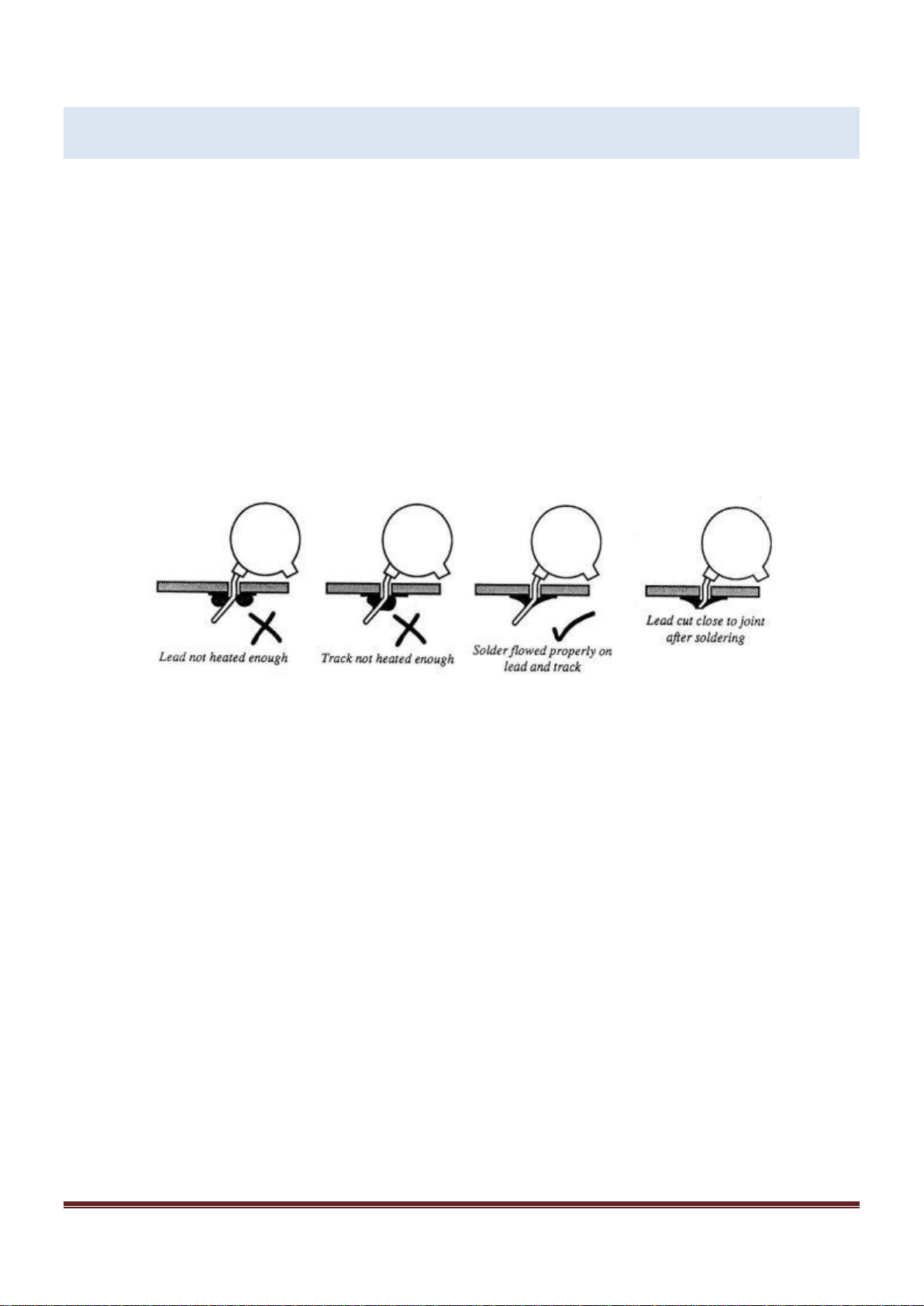
Soldering:
There are two essential things to keep in mind to ensure the proper functioning of a kit. The first is to put
the component into its proper place on the circuit board, the second is good soldering.
To solder properly, you must use a high-quality solder for electronics and the correct type of soldering
iron. Use a small soldering iron that has a fine, pointed tip. The soldering iron should be about 30 watts
(if it is not thermostatically controlled). Use only solder intended for electronic soldering; NEVER use
extra flux. You should hold the hot soldering iron in contact with both the circuit board and the
component lead for about two seconds to heat them up. Then, keeping the soldering iron in place, touch
the solder at the junction of the component lead and circuit board trace and wait about two seconds or so
until the solder flows between the lead and the trace to form a good joint. Now remove the soldering iron.
The soldering iron should have been in contact with the joint for a total time of about 4 seconds. After
soldering each joint, you should clean the soldering tip, removing any excess solder. This prevents
mixing in old solder and residues from previous soldering operations.
Finding the correct component:
IC’s
The component outline for the IC printed on the circuit board has a “U” shaped notch on one end,
indicating the end at which pin 1 of the IC is located. There is a similar notch on one end of the IC socket
that should be oriented over the “U” printed on the circuit board. Finally, pin 1 of the IC is also marked
with a small dimple or dot; this end of the IC should be oriented towards the notch in the IC socket or the
"U" of the component outline.

DB4020 Dual Band 40&20M SSB QRP Transceiver Kit Page 6
Diodes
Be careful to observe the correct polarity of the diodes. There is a dark-colored band towards one end of
the diode. This band should be oriented towards the line printed on the component outline of the circuit
board.
Electrolytic capacitors:
These must be placed with the correct polarity. The positive lead (+) is always the long lead. The
negative terminal (-) is the short lead and is marked by a stripe on the body of the capacitor. Make sure
that the positive lead of the capacitor goes through the hole marked with a "+" on the circuit board.
Toroids:
You may find it convenient to wind and prepare all the toroids before beginning to mount the
components. That way you won't have to stop and possibly lose concentration while winding them.
This is the part of the construction that some consider to be the most difficult. I personally find it to be
one of the easiest stages, and it can even be relaxing. Look for the most appropriate moment to do it,
and most importantly, take your time. The drawings, photos and instructions in the manual will illustrate
and make the process easier.

DB4020 Dual Band 40&20M SSB QRP Transceiver Kit Page 7
LIST OF COMPONENTS BY VALUE/QUANTITY
Resistor list
Qty
Value
Checked
Ref.
Identified
2
1Ω
R39, R58
brown-black-gold
3
10Ω
R40,R41,R50
brown-black-black
7
22Ω
R6,R8,R18,R29,R31,R60,R61
red-red-black
6
100Ω
R10,R12,R13,R15,R37,R52
brown-black-brown
2
150Ω
R51,R53
brown-green-brown
2
330Ω
R17, R20
orange-orange-brown
5
470Ω
R1,R7,R30,R42,R49
yellow-violet-brown
7
1K
R11,R14,R22,R24,R32,R33,R59,
brown-black-red
1
1K5
R19
brown-green-red
4
4K7
R5,R9,R16, R44
yellow-violet-red
11
10K
R4, R34, R35, R38, R45, R46, R47, R48, R54, R56, R57
brown-black-orange
1
22K
R55
red-red-orange
3
47K
R2, R3, R43
yellow-violet-orange
4
100K
R23, R25, R26, R27
brown-black-yellow
2
220K
R28, R36
red-red-yellow
3
10K
P1, P2, P4 adjustable trimmer
103
1
100K
P6 adjustable trimmer
104
1
1K
P3 potentiometer 1K
B1K
1
10K
P5 potentiometer 10K
B10K
1
Encoder
Rotary Encoder PEC16-2015F
--
Capacitors list
Qty
Value
Checked
Ref.
Identified
8
1n
C2,C5,C18,C20,C21,C22,C55,C78
102 or 0.001
4
10n
C26,C27,C30,C81
103 or 0.01
43
100n
C6,C8,C9,C15,C16,C19,C23,C24,C28,C29,C31,C32,C33,
C34,C49,C50,C52,C53,C54,C56,C58,C59,C61,C63,C69,C70
C72,C73,C74,C75,C79,C80,C84,C86,C88,C89,C92,C94,C98,
C99,C100,C101,C107
104 or 0.1
2
470n
C1,C3
474 or 0.47
1
1p5
C96
1P5 or 1.5
2
8p2
C44,C47
8P2 or 8.2
1
15p
C93
15P or 15J
1
22p
C60
22P or 22J
7
33p
C10,C11,C12,C13,C14,C64,C68
33P or 33J
5
82p
C43,C45,C46,C48,C95
82P or 82J
2
220p
C17,C62
n22 or 221 or 220
2
180p
C39,C42 Polystyrene
180
2
270p
C35,C38 Polystyrene
270
2
390p
C40,C41 Polystyrene
390
2
680p
C36,C37 Polystyrene
680
2
1uf
C4, C57 (elect.)
1uf
1
4u7
C90 (elect.)
4.7uf
8
10uf
C7, C25, C51, C76, C77, C82, C97, C102 (elect.)
10uf
1
47uf
C91 (elect.)
47uf
3
100uf
C71, C83, C85 (elect.)
100uf
1
220uf
C87 (elect.)
220uf

DB4020 Dual Band 40&20M SSB QRP Transceiver Kit Page 8
Semiconductor list
Qty
Type
Checked
Ref.
Identified
Transistors
1
P2222
Q1
2222
1
BD135
Q2
BD135
1
2SC1969
Q3
2SC1969
5
BC547
Q4, Q7, Q8, Q9, Q11
BC547
2
2N7000
Q5,Q6
2N7000
1
BC557/8
Q10
BC558 or BC558
Integrated circuits
4
NE602SG
IC1,IC2,IC4,IC5
NE602 or SA602
1
LM386
IC7
LM386
1
UA741
IC6
741
1
78L05
IC3
78L05
1
7805
IC9
7805
1
7809
IC8
7809
1
SI5351
IC10
SI5351
1
DISPLAY OLED 1.3”
IC11
--
1
ARDUINO NANO
IC12
--
Diodes
15
1N4148
D4,D5,D7,D8,D9,D10,D11,D12,D13,D14,D15, D16,
D17,D18,D20
4148
2
Zener 6V2
D1,D6
6V2
1
Zener 1W 47V
D3
47V
1
1N4001/7
D2
4001 or 4007
1
BY255
D19
BY255
Inductor/RF Transformer/Crystal/Relay list
Qty
Value
Checked
Ref.
Identified
2
1u2H
L4,L5
1u2 or 1R2
2
5u3H
L2,L3
5u3 or 5R3
2
100uH
L1,L7
brown black brown
3
T37-2
L9, L10, L11
Red toroid
3
T37-6
L12, L13, L14
Yellow toroid
2
FT37-43
L6, L8
Black toroid
8
4.915MHz.
4.915MHz crystals
4.915 or 4.91
1
12VDPDT Relay
RL1
Huigang HRS2H 12V
7
OMRON G5V-1 12V
RL2,RL3,RL4,RL5,RL6,RL7,RL8
Omron G5V-1 12V
Connectors and Hardware
Qty
Value
Checked
Ref.
Identified
1
BNC socket
BNC PCB socket
--
2
Jack socket
Stereo PCB Jack 3.5mm socket
--
1
Supply socket
Power supply PCB Jack 2.1mm socket
--
2
Switch
SPDT PCB switch toggle
--
2
Female pins
15 pin female sockets strip (Arduino)
--
1
Male pins
5 pin male strippolarized socket
--
6
IC sockets
8 pins IC sockets
--
11
Male pins strip
4 + 3 + 2 + 2 nopolarizedstrip pins
--
2
45° strip pins
7 pin 45° bent strip (to SI5351 module)
--
4
Jumper
Jumpers to J1, J2 and J3, J4 (IF Rx filter jumpers).
--
1
Heatsink
Heatsink to Q3
--
1
Heatsink
Heatsink to Q2
--
2
Mica insulator
Mica insulator to Q2 and Q3
--

DB4020 Dual Band 40&20M SSB QRP Transceiver Kit Page 9
1
Plastic washer
Plastic through isolator washer to Q3 screw
--
2
M3x10 screw
10mm M3x10 screw to Q3 and Q2
--
4
M3x4 screws
4mm M3x4 screws
--
6
M3 nuts
M3 nuts
--
2
M3 washer
Metal M3 washer to Q2 and Q3
--
4
M3 spacers
Hex 5mm M3 spacers
--
217
217 cms.
217 cms. 0,5mm enamelled wire
--
1
Microphone
Electret Microphone Capsule
--
1
PCB
DB4020 PCB (printedcircuitboard)
DB4020

DB4020 Dual Band 40&20M SSB QRP Transceiver Kit Page 10
LIST OF INDIVIDUAL COMPONENTS
Resistors
Checked
Ref.
Value
Ident./Comment
Circuit section
Located
R1
470 Ω
yellow-violet-brown
Microphone input
N-2
R2
47K
yellow-violet-orange
SSB gen balance
M-2/3
R3
47K
yellow-violet-orange
SSB gen balance
M-4
R4
10K
brown-black-orange
Mic supply
N-1
R5
4K7
yellow-violet-red
Mic. Supply
N-1
R6
22 Ω
red-red-black
IC1 supply
L-2/3
R7
470 Ω
yellow-violet-brown
IC1 and IC2 supply
K-1
R8
22 Ω
red-red-black
IC2 supply
M-4
R9
4K7
yellow-violet-red
Pre-driver
L-4/5
R10
100 Ω
brown-black-brown
Pre-driver
K-4/5
R11
1K
brown-black-red
Pre-driver
L-4
R12
100 Ω
brown-black-brown
Pre-driver
L-4
R13
100 Ω
brown-black-brown
Pre-driver
K-2
R14
1K
brown-black-red
Driver
J-2
R15
100 Ω
brown-black-brown
Driver
J-1/2
R16
4K7
yellow-violet-red
Driver
J-3/4
R17
330 Ω
orange-orange-brown
Driver
J-1/2
R18
22 Ω
red-red-black
Driver
J-4/5
R19
1K5
brown-green-red
Output Amp bias
H-3
R20
470 Ω
yellow-violet-brown
Output Amp
G/H-2
R21
No used
--
BPF
H-5
R22
1K
brow-black-red
BPF
H-7
R23
100K
brown-black-yellow
AGC
D-10
R24
1K
brown-black-red
AGC
E-10
R25
100K
brown-black-yellow
AGC
F-10
R26
100K
brown-black-yellow
AGC
F-10
R27
100K
brown-black-yellow
AGC
F-11
R28
220K
red-red-yellow
AGC
F-11
R29
22 Ω
red-red-black
IC4 supply
L-9
R30
470 Ω
yellow-violet-brown
IC4 and IC5 supply
K-9/10
R31
22 Ω
red-red-black
IC5 supply
M-10
R32
1K
brown-black-red
SSB Dem
N-11
R33
1K
brown-black-red
Audio preamp
M-11
R34
10K
brown-black-orange
Audio preamp
K-11
R35
10K
brown-black-orange
Audio preamp
K-11
R36
220K
red-red-yellow
Audio preamp
J-11
R37
100 Ω
brown-black-brown
IC6 supply
J-11/12
R38
10K
brown-black-orange
Audio Amp
M-12
R39
1 Ω
brown-black-gold
Audio Amp
L-13
R40
10 Ω
brown-black-black
Audio Amp
N-13
R41
10 Ω
brown-black-black
Audio Amp
O-13
R42
470
yellow-violet-brown
S-Meter
K-12
R43
47K
yellow-violet-orange
S-Meter
P-13
R44
4K7
yellow-violet-red
S-Meter
Q-13
R45
10K
brown-black-orange
Mute
O-12
R46
10K
brown-black-orange
Mute
P-12
R47
10K
brown-black-orange
Band switch
D-13/14
R48
10K
brown-black-orange
Band switch
C-13/14
R49
470 Ω
yellow-violet-brown
VFO input
O-7
R50
10 Ω
brown-black-black
BFO input
O-8
R51
150 Ω
brown-green-brown
BFO input
O-8/9
R52
100 Ω
brown-black-brown
BFO input
O-9
R53
150 Ω
brown-green-brown
BFO imput
O-9
R54
10K
brown-black-orange
Arduino nano
Q-8

DB4020 Dual Band 40&20M SSB QRP Transceiver Kit Page 11
R55
22K
red-red-orange
Arduino nano
Q-9
R56
10K
brown-black-orange
Rotary encoder
Q-5
R57
10K
brown-black-orange
Rotary encoder
Q-6
R58
1 Ω
brown-black-gold
Tx SSB supply
I-9/10
R59
1K
brown-black-red
CW Tx Mute
D-12
R60
22 Ω
red-red-black
Headphones Att.
A-5
R61
22 Ω
red-red-black
Headphones Att.
A-4
P1
10K
adjustable resistor 103
Mic gain
N-2
P2
10K
adjustable resistor 103
DSB balance
M-3
P3
1K
Potentiometer B1K
RX atennuator
R-12/13
P4
10K
adjustable resistor 103
AGC gain
C-10
P5
10K
Potentiometer B10K
Volume
R-10/11
P6
100K
adjustable resistor 104
S-Meter
P-12
Encoder
--
Rotary Encoder PEC16-4015F
VFO Tune
R-7
Capacitors
Checked
Ref.
Value
Ident./Comment
Circuit section
Located
C1
470n
474 or 0.4
Microphone input
M-1
C2
1n
102 or 0.001
Microphone input
M-2
C3
470n
474 or 0.4
Microphone input
M-2
C4
1uF
1uF electrolytic
SSB balance
M-4
C5
1n
102 or 0.001
Microphone supply
L-2
C6
100n
104 or 0.1
Microphone supply
O-2
C7
10uF
10uF electrolytic
Microphone supply
O-2
C8
100n
104 or 0.1
IC1 supply
M-4
C9
100n
104 or 0.1
IC1 an d IC2 supply
K-1
C10
33p
33 or 33J
IF xtal filter
O-4
C11
33p
33 or 33J
IF xtal filter
N-4
C12
33p
33 or 33J
IF xtal filter
N-6
C13
33p
33 or 33J
IF xtal filter
M-6
C14
33p
33 or 33J
IF xtal filter
M-5
C15
100n
104 or 0.1
TX mix
M-6
C16
100n
104 or 0.1
IC2 supply
K-5
C17
220p
n22 or 222 or 221
TX mix
K-6
C18
1n
102 or 0.001
Pre driver
L-5
C19
100n
104 or 0.1
Pre driver
K-5
C20
1n
102 or 0.001
Pre driver
K-4
C21
1n
102 or 0.001
Driver
G/H-10
C22
1n
102 or 0.001
Driver
F-5
C23
100n
104 or 0.1
Driver
J-1
C24
100n
104 or 0.1
Driver supply
I-1
C25
10uF
10uF electrolytic
Driver supply
I-2
C26
10n
103 or 0.01
Driver
K-3
C27
10n
103 or 0.01
Driver
I-4
C28
100n
104 or 0.1
Output Amp
G/F-3
C29
100n
104 or 0.1
Output Amp bias
G/F-4
C30
10n
103 or 0.01
Output Amp
G-1/2
C31
100n
104 or 0.1
Output Amp
F-4/5
C32
100n
104 or 0.1
Rx Ant path
D-3
C33
100n
104 or 0.1
Output Amp supply
E-3
C34
100n
104 or 0.1
Output Amp supply
H-4
C35
270p
Polystyrene 270J
40m LPF
C-5
C36
680p
Polystyrene 680J
40m LPF
D-5
C37
680p
Polystyrene 680J
40m LPF
D/E-5
C38
270p
Polystyrene 270J
40m LPF
E-5
C39
180p
Polystyrene 180J
20m LPF
C-7
C40
390p
Polystyrene 390J
20m LPF
D-7
C41
390p
Polystyrene 390J
20m LPF
D/E-7
C42
180p
Polystyrene 180J
20m LPF
E-7
C43
82p
82
40m BPF
H-5

DB4020 Dual Band 40&20M SSB QRP Transceiver Kit Page 12
C44
8p2
8p2
40m BPF
H-6
C45
82p
82
40m BPF
H-5
C46
82p
82
20m BPF
H-7
C47
8p2
8p2
20m BPF
H-8
C48
82p
82
20m BPF
H/I-7
C49
100n
104 or 0.1
AGC
G-10
C50
100n
104 or 0.1
AGC supply
G-12
C51
10uF
10uF electrolytic
AGC supply
G-10/11
C52
100n
104 or 0.1
AGC supply
H-11
C53
100n
104 or 0.1
AGC
C-11
C54
100n
104 or 0.1
AGC
C-10
C55
1n
102 or 0.001
AGC
D-11
C56
100n
104 or 0.1
AGC
E-10
C57
1uF
1uF electrolytic
AGC
E-11
C58
100n
104 or 0.1
AGC
G-10
C59
100n
104 or 0.1
AGC
G-8/9
C60
22p
22
RX Mix
K-8
C61
100n
104 or 0.1
RX Mix
K-7
C62
220p
n22 or 222 or 221
RX Mix
L-7
C63
100n
104 or 0.1
IC4 supply
L-9
C64
33p
33
IF xtal filter
M-9
C65
33p
SMD pre-soldered on bottom
IF xtal filter
(M-7)
C66
33p
SMD pre-soldered on bottom
IF xtal filter
(N-7)
C67
33p
SMD pre-soldered on bottom
IF xtal filter
(N-8)
C68
33p
33
IX xtal filter
N-8
C69
100n
104 or 0.1
SSB Dem
N-9
C70
100n
104 or 0.1
IC4 and IC5 supply
L-10
C71
100uF
100uF electrolytic
IC4 and IC5 supply
L/M-10
C72
100n
104 or 0.1
IC4 and IC5 supply
J-10
C73
100n
104 or 0.1
IC5 supply
M-10
C74
100n
104 or 0.1
Audio preamp
M-11/12
C75
100n
104 or 0.1
Audio preamp
M-11
C76
10uF
10uF electrolytic
Audio preamp
L-11
C77
10uF
10uF electrolytic
Audio preamp
K-12
C78
1n
102 or 0.001
Audio preamp
J-11
C79
100n
104 or 0.1
S-Meter path
J-12
C80
100n
104 or 0.1
Audio Amp path
J-12
C81
10n
103 or 0.01
Audio Amp
L-12
C82
10uF
10 uFelectrolytic
Audio Amp
K-13
C83
100uF
100uF electrolytic
Audio Amp
L-14
C84
100n
104 or 0.1
Audio Amp
M-13
C85
100uF
100uF electrolytic
Audio Amp out
M-14
C86
100n
104 or 0.1
Power supply
A-2
C87
220uF
220uF electrolytic
Power supply
B-1
C88
100n
104 or 0.1
CW Mute
D-12
C89
100n
104 or 0.1
S-Meter
Q-13
C90
4u7F
4.7uF electrolytic
S-Meter
P-12/13
C91
47uF
47uF electrolytic
Mute
O-11/12
C92
100n
104 or 0.1
Band switch
C-14
C93
15p
15
VFO input
O-7
C94
100n
104 or 0.1
BFO input
O-8
C95
82p
82
RX BFO path
N/O-9
C96
1p5
1p5
TX BFO path
O-9
C97
10uF
10uF electrolytic
Arduino nano
Q-11
C98
100n
104 or 0.1
Arduino nano
Q-11
C99
100n
104 or 0.1
Arduino nano
Q-8
C100
100n
104 or 0.1
Si5351
J-9/10
C101
100n
104 or 0.1
SI5351
Q-9
C102
10uF
10uF electrolytic
Arduino nano
R-9
C103
100n
SMD pre-soldered on bottom
Arduino nano
(R-3)
C104
100n
SMD pre-soldered on bottom
Arduino nano
(R-6)
C105
100n
SMD pre-soldered on bottom
Arduino nano
(R-7)
C106
100n
SMD pre-soldered on bottom
Arduino nano
(Q-2)

DB4020 Dual Band 40&20M SSB QRP Transceiver Kit Page 13
Crystals
Checked
Ref.
Frequency
Ident./Comment
Circuit section
Located
X1
4.915 MHz
4.915 or 4.91
TX IF xtal filter
O-4
X2
4.915 MHz
4.915 or 4.91
TX IF xtal filter
O-6
X3
4.915 MHz
4.915 or 4.91
TX IF xtal filter
N-6
X4
4.915 MHz
4.915 or 4.91
TX IF xtal filter
N-4
X5
4.915 MHz
4.915 or 4.91
RX IF xtal filter
M-8
X6
4.915 MHz
4.915 or 4.91
RX IF xtal filter
M-7
X7
4.915 MHz
4.915 or 4.91
RX IF xtal filter
N-7
X8
4.915 MHz
4.915 or 4.91
RX IF xtal filter
N-9
Semiconductors
Checked
Ref.
Type
Ident./Comment
Circuitsection
Located
Transistors
Q1
P2222
2222
Pre driver
K-3
Q2
BD135
BD135
Driver
I-3/4
Q3
2SC1969
2SC1969
PA output TX amp
G-2
Q4
BC547
BC547
AGC
D-10
Q5
2N7000
2N7000
AGC
G-10
Q6
2N7000
2N7000
AGC
G-10
Q7
BC547
BC547
S-Meter
Q-14
Q8
BC547
BC547
Mute
N-12
Q9
BC547
BC547
Band switch
C-13
Q10
BC557/8
BC557 or BC558
Band switch
B-13
Q11
BC547
BC547
CW Mute
C-12
IC's
IC1
NE602
NE602 or SA602
SSB Gen
N-3
IC2
NE602
NE602 or SA602
TX Mix
L-5/6
IC3
78L05
78L05
AGC supply
G-11
IC4
NE602
NE602 or SA602
RX Mix
L-7/8
IC5
NE602
NE602 or SA602
SSB Dem
N-10
IC6
UA741
741
Audio premp
J/K-11
IC7
LM386
LM386
Audio Amp
L/M-13
IC8
7809
7809
Arduino supply
P-10
IC9
7805
7805
Arduino supply
R-9
IC10
SI5351 Module
SI5351
SI5351
R-8/9
IC11
DISPLAY OLED
1.3” display
Display
R2/3
IC12
ARDUINO NANO
--
Arduino nano
P/Q-1/5
C107
100n
104 or 0.1
Arduino nano
Q-11/12
C108
100n
SMD pre-soldered on bottom
Arduino nano
(P-5)
C109
100n
SMD pre-soldered on bottom
Arduino nano
(Q-1/2)
C110
100n
SMD pre-soldered on bottom
Arduino nano
(Q-1/2)
Diodes
D1
6V2
6.2V Zener diode
IC1 and IC2 supply
L-2
D2
1N4001/7
1N400 or 1N4407
Output Amp bias
H-2
D3
1W47V
47V Zener diode
Output Amp
F-3
D4
1N4148
4148
AGC
E-10/11
D5
1N4148
4148
AGC
E-11
D6
6V2
6.2V Zener diode
IC4 and IC5 supply
K-9/10
D7
1N4148
4148
S-Meter
Q-13
D8
1N4148
4148
S-Meter
Q-12
D9
1N4148
4148
RIT path
O-1/2

DB4020 Dual Band 40&20M SSB QRP Transceiver Kit Page 14
Inductors/RF Transformers/Relay
Checked
Ref.
Value/Type
Ident./Comment
Circuit section
Located
L1
100uH
brown black brown
Pre-driver
L-2/3
L2
5u3H
5u3 or 5R3
40m BPF
G-6
L3
5u3H
5u3 or 5R3
40m BPF
I-6
L4
1u2H
1u2 or 1R2
20m BPF
G-7
L5
1u2H
1u2 or 1R2
20m BPF
I-7
L6
FT37-43
Black toroid
Driver output
H-3
L7
100uH
brown black brown
Output amp bias
G-4
L8
FT37-43
Black toroid
Output amp out
F-3/4
L9
T37-2
Red toroid
40m LPF
C-6
L10
T37-2
Red toroid
40m LPF
D-6
L11
T37-2
Red toroid
40m LPF
E-6
L12
T37-6
Yellow toroid
20m LPF
C-8
L13
T37-6
Yellow toroid
20m LPF
D-8
L14
T37-6
Yellow toroid
20m LPF
E-8
Relés
RL1
RL1a/b
Huigang HRS2H 12V
Power/ant. relay
C/D-3
RL2
RL2
Omron G5V-1 12V
Mute
N-13
RL3
RL3
Omron G5V-1 12V
Band switch
D-4
RL4
RL4
Omron G5V-1 12V
Band switch
D-8/9
RL5
RL5
Omron G5V-1 12V
Band switch
F-6
RL6
RL6
Omron G5V-1 12V
Band switch
J-5
RL7
RL7
Omron G5V-1 12V
TX / RX path
F-8
RL8
RL8
Omron G5V-1 12V
TX / RX path
J-8
D10
1N4148
4148
Mute
P-5/6
D11
1N4148
4148
Mute
P-13
D12
1N4148
4148
Mute
O-12
D13
1N4148
4148
Relay RL2
O-13
D14
1N4148
4148
Mute
N-12
D15
1N4148
4148
PTT path
C/D-1
D16
1N4148
4148
Relay RL1
C/D-1
D17
1N4148
4148
Relays 3,4, 5, 6
E-8/9
D18
1N4148
4148
Relays 7, 8
E-8/9
D19
BY255
BY255
Power supply protect
A-4
D20
1N4148
4148
Arduino nano
Q-9

DB4020 Dual Band 40&20M SSB QRP Transceiver Kit Page 15
252-QUADRANT COMPONENT LAYOUT MAP

DB4020 Dual Band 40&20M SSB QRP Transceiver Kit Page 16
ASSEMBLY
You can use the “individual parts list” or the “value/quantity parts list.” Using the “value/quantity parts list”
is the quickest way to mount components since all the circuit board components of the same value or
type can be placed one after the other. However, you will need the “individual parts list” to know how
each component is identified and its location on the circuit board. Depending on your personal
experience, you may prefer the individual parts list and feel more confident using it.
The 252-quadrant component layout map makes it very easy to find the location for all the components.
After mounting each component, it can be marked off in the “checked” column.
It is highly recommended that an inventory be taken of all the components to make sure that everything
can be located and is ready for assembly. Each builder may have his/her own method of organizing the
components. One suggested method is to use a block of Styrofoam packing material and poke the
components into it. The components can be sorted by type, value and size (ohms, micro-farads etc.).
RECOMMENDED ASSEMBLY SEQUENCE
Resistors
The resistors are installed first. Mount all resistors and trimmers P1, P2, P4 and P6
P3 and P5 are the RF attenuator and volume potentiometers respectively; which should not be installed
yet.
Refer to the parts list, and select the first resistor, R1. Bend the leads as close to the component body as
possible (otherwise, they will not fit well into the holes), and place them into the appropriate holes
according to the component outline printed on the circuit board. Be careful to avoid confusing the
resistors with the axial inductors which are a bit thicker.
All of the resistors have a light-colored body and a gold band on one end. Inserting the resistor leads into
the holes, push down on the body of the component so that it rests flat on the board, hold it in place, and
then slightly bend the leads to keep the resistor in place. Then turn the board over and solder the leads
to the printed circuit trace. Make sure that the resistor body lies flat on the board so that its leads are as
short as possible. Please read the notes about soldering, as poor soldering is the most common cause
for a kit failing to work for the first time. After soldering the component leads, cut off the excess length as
close to the joint as possible. Mount the next resistor in the parts list in the same manner and continue
until all the resistors are mounted.
The values which are in decade increments can be easily confused, such as 470, 4K7 and 47K, so be
sure to verify the colors before soldering the component in place! If you are in doubt, use a multimeter to
check the resistance value.

DB4020 Dual Band 40&20M SSB QRP Transceiver Kit Page 17
Axial Inductors
These components look like thick-bodied resistors and the body is colored blue or green. In their interior
there is a small coil wound on a ferrite core. There are two axial inductors L1 and L7, refer to the parts
list to select the correct component for each location. Mount the inductors in their respective locations, as
identified on the circuit board, in the same manner as you did with the resistors.
Diodes
Next mount the diodes, being careful to place them with the correct orientation. There is a dark-colored
band on one end of each diode that corresponds to the component outline on the circuit board. There
are 15 1N4148 diodes; they are normally orange in color with a black band and they have the type
“4148” printed on the body. Note that some diodes are mounted in a vertical position.
D1 and D6 are Zener diodes, similar in size to 1N4148 but are marked 6V2.
D2 is a 1N4001 or 1N4007 diode; it is mounted vertically to the side of Q3. It should be at the same
height as Q3 as shown in the image.
D3 is also a Zener diode (thicker than the others); it is marked 47V.
Diode D19 is a BY255, black, much thicker than the others.

DB4020 Dual Band 40&20M SSB QRP Transceiver Kit Page 18
Capacitors
There are ceramic, polystyrene (Styroflex) and electrolytic capacitors. They all have their value printed
on the body. Refer to the “identified” column in the parts list.
When you mount them, make sure to leave the leads as short as possible.
C35 through C42 are polystyrene capacitors; these are axial capacitors, but they must be mounted in a
vertical position (see image).
The values which are in decade increments can be easily confused, such as 100n and 10n, so be sure
to verify the numbers of their value before soldering them in place!
The electrolytic capacitors must be placed with the correct orientation: the LONG LEAD goes in the hole
labeled “+” and the SHORT LEAD is "-", indicated by a band containing "-" signs on the side of the
capacitor.

DB4020 Dual Band 40&20M SSB QRP Transceiver Kit Page 19
Pin headers and jumpers
Place and solder the 5-pin header corresponding to the microphone and speaker.
Place and solder the pin headers “J1” and “J2”
Place and solder 4 pins strip on RX IF crystal filter input.
Place and solder 3 pins strip on RX IF crystal filter output
Place and solder 2 x female 15 pin strips for the Arduino UNO.
Turn the board over and use one hand to insert and hold the header in place, using a “jumper” placed on
the header while you solder the pins to avoid burning your fingers. Use your other hand to hold the
soldering iron and move the board towards the solder to solder the headers in place. If you have
someone available to help you, it will be much easier!
Place jumpers on the terminals:
- “J1” if you do not use an ON/OFF switch.
- “J2” if you do not use the optional CW module.
- “RX IF Filter jumpers”if you no use the optional CW Interface and filter (see images)
Jumper on RX IF crystal filter input Jumper on RX IF crystal filter output

DB4020 Dual Band 40&20M SSB QRP Transceiver Kit Page 20
Transistors
All of the transistors have their type printed on the component body. Place them according to the
corresponding component outline printed on the circuit board.
Be very careful not to confuse the types. Although their body is the same but they are different
transistors. Use a suitable magnifying glass to read the marked references printed on them.
Q2 BD135
Mount Q2 onto the heatsink as shown in the image.
Use a mica insulator sheet that you will find in the kit and trim it 1-2mm so that it seats well within the
heatsink.
Q3 2SC1969
Mount Q3 (TX power amplifier) onto the heatsink as shown in the image. This transistor is placed with a
mica insulator sheet and also a heatsink insulator bushing that insulates the screw from the transistor
body. This is an important task; it should be done exactly as shown in the images.
Other manuals for DB4020
1
Table of contents
Other EA3GCY Transceiver manuals