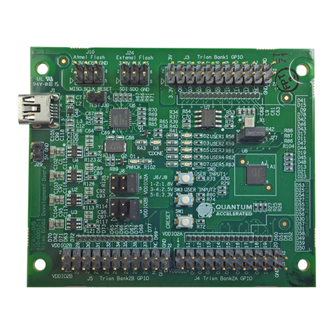
Efinix Trion8 BGA81 User manual

Trion™ 8 BGA81
Development Kit User Guide
T8F81C-DK-UG-v1.0
June 2018
www.efinixinc.com
Copyright © 2018. All rights reserved. Efinix, the Efinix logo, Quantum, Trion, and Efinity are trademarks of Efinix, Inc. All other trademarks and service
marks are the property of their respective owners. All specifications subject to change without notice.

Contents
Overview........................................................................................................................................................................... 3
What's in the Box?....................................................................................................................................................... 3
Software Requirements...............................................................................................................................................3
Installing Standoffs.........................................................................................................................................................3
Running the Demonstration Design........................................................................................................................... 3
Board Functional Description...................................................................................................................................... 4
Features...........................................................................................................................................................................5
Overview......................................................................................................................................................................... 5
Power On........................................................................................................................................................................6
Reset.................................................................................................................................................................................7
Clock Sources................................................................................................................................................................7
Headers........................................................................................................................................................................... 8
User Outputs................................................................................................................................................................. 11
User Inputs.....................................................................................................................................................................11
Creating Your Own Design..........................................................................................................................................11
Revision History.............................................................................................................................................................12

Trion 8 BGA81 Development Kit User Guide
Overview
Thank you for choosing the Trion™ 8 BGA81 Development Kit (part number:
T8F81C-DK), which allows you to explore the features of the T8 FPGA.
Warning: The board can be damaged without proper anti-static handling.
What's in the Box?
The Trion™ 8 BGA81 Development Kit includes:
•Trion™ 8 BGA81 Development Board preloaded with a demonstration design
•4 standoffs
•4 screws
•3 foot mini-USB cable (type B)
Software Requirements
To develop your own designs for the T8 device on the board, you must install the
Efinity™ software. You can obtain the software from the Efinix™ Support Center
under Downloads (www.efinixinc.com/support/).
Note: The Efinity™ software includes tools to program the device on the
board. Refer to the Efinity™ Software User Guide for information about
how to configure the device.
Learn more: Efinity™ documentation is installed with the software (see
Help > Documentation) and is also available in the Support Center
under Docs.
Installing Standoffs
Before using the board, attach the 4 standoffs to the board with the screws
provided in the kit.
Warning: The board can be damaged if you over tighten the
screws. Tighten all screws to a torque between 4 ± 0.5 kgf/cm and
5 ± 0.5 kgf/cm.
Running the Demonstration Design
Efinix™ preloads the Trion™ 8 BGA81 Development Board with a demonstration
design that operates the LEDs. The board receives power through USB cable.
Follow these steps to run the design:
1. Connect the USB cable to the board and to your computer. LED D1 turns
on briefly and then turns off, indicating that the board is receiving power
correctly. All other LEDs are turned off.
www.efinixinc.com 3

Trion 8 BGA81 Development Kit User Guide
When configuration completes, the configuration done LED (D8) turns
on briefly and then turns off. Four green LEDs (D2, D3, D5, D6) turn on,
sweeping in one direction.
Note: If LED D1 does not turn off, the board is not receiving power
correctly from the computer via the USB cable.
2. Press and hold pushbutton SW3. The LED sweep direction changes and LED
D7 turns on.
3. Press and hold pushbutton SW2 (reset) to turn off all LEDs.
Board Functional Description
The Trion™ 8 BGA81 Development Board contains a variety of components to
help you build designs for the Trion™ T8 device.
Figure 1: Trion™ 8 BGA81 Development Board Block Diagram
Efinix
T8F81C
WINBOND 8 Mbit
SPI NOR Flash
8 MHz
PLL IN
Low Dropout
Regulators
(Max 180 mA)
1.1 V
1.8 V
2.5 V
3.3 V
Voltage
Select
Voltage
Select
T8F81C
VDDIO 2A
T8F81C
VDDIO 2B
T8F81C
Bank 1A
Bank 1B
Header
3.3 V
T8F81C
VDDIO 2B
GND
User LEDs
x5
Bank 2A GPIO
External Flash
Programming
Atmel Internal
Flash Programming
1.1 V
Atmel
Microcontroller
SS
SCK
MOSI
(CD0)
MISO
(CD1)
CRESET
CDONE
SS
SCK
MOSI
MISO
PB6
PB7
33.333 mHz
SS SCK SDISDO
Jumper
USB Power 5 V
RESET
Power Good
GND
Bank 1A / 1B GPIO
CRESET
Pushbutton
CDONE
LED
User Inputs
x2
T8F81C
Bank 2A
Header
T8F81C
Bank 2B
Header
Bank 2B GPIO
T8F81C
VDDIO 2A
GND
3.3 V
3.3 V
2.5 V
1.8 V
3.3 V
2.5 V
1.8 V
VDDIO 1A
VDDIO 1B
VDDIO 2A
VDDIO 2B
CORE
USART
(SPI MODE)
HOLD
PC4..7
PB4
Header
USB
Data
Mini-USB
Connector
www.efinixinc.com 4

Trion 8 BGA81 Development Kit User Guide
Features
•Compact design (76.2 x 63.5 mm)
•Efinix™ T8F81C device in an 81-ball FineLine BGA package
•Atmel microcontroller with built-in USB controller
•Winbond 8 Mbit SPI NOR flash memory
•Mini-USB 2.0 type B receptacle
•Power source: USB 5 V, 500 mA USB
•On-board low dropout regulators (maximum at 180 mA) source 3.3 V and
2.5 V components. The 5 V USB sources the 1.8 V and 1.1 V components.
•Selectable 3.3 V, 2.5 V, and 1.8 V VDDIO for T8F81C I/O banks 2A and 2B
•Fixed 3.3 V VDDIO for T8F81C I/O banks 1A and 1B
•33.333 MHz oscillator for T8F81C PLL input
Note: Optionally, the user can drive the PLL input via a pin in the
T8F81C bank 1B I/O header. See Clock Sources on page 7 for
details.
•5 LEDs on T8F81C bank 1A and 1B I/O pins for user outputs
•2 pushbutton switches connected to T8F81C bank 1A I/O pins for user inputs
•Power good and T8F81C configuration done LEDs
•5 V USB header to provide power for external devices
Overview
The board features the Efinix™ T8 programmable device, which is fabricated
using Efinix™ Quantum™ technology. The Quantum™-accelerated programmable
logic and routing fabric is wrapped with an I/O interface in a small footprint
package. T8 devices also include embedded memory blocks and multiplier blocks
(or DSP blocks). You create designs for the T8 device in the Efinity™ software, and
then download the resulting configuration bitstream to the board using the USB
connection.
Note: For more information on T8 FPGAs, refer to the T8 Data
Sheet, which you can download in our Support Center under Docs
(www.efinixinc.com/support/).
www.efinixinc.com 5

Trion 8 BGA81 Development Kit User Guide
Figure 2: Trion™ 8 BGA81 Development Board Components
Trion T8F81C
Device
SPI NOR Flash
Atmel
Microcontroller
On-Board
Low Dropout
Regulators
Oscillator Clock
33.333 MHz
Bank 1A/1B
GPIO (J3)
Select PLL Input
Source (J27)
Mini-USB
Type B
Voltage Select
for Bank 2B
VDDIO (J8)
Voltage Select
for Bank 2A
VDDIO (J6)
Bank 2A
GPIO (J4)
Bank 2B
GPIO (J5)
User LEDs
User Pushbuttons
Power
OK LED
CDONE
LED
Reset Pushbutton
5 V Power for
External Devices
The Atmel microcontroller has a built-in USB controller; it receives the T8
configuration bitstream from a USB host and writes to the on-board SPI NOR
flash memory. The microcontroller can also write the configuration bitstream
directly to the device when it is configured to boot in passive mode.
The SPI NOR flash memory stores the configuration bitstream it receives from
the microcontroller. The T8 device accesses this configuration bitstream when it is
in active configuration mode (default).
The board's main power supply is the 5 V DC (500 mA) it receives from the USB
interface. The board regulates down the 5 V DC using on-board low dropout
regulators to provide the necessary voltages for the T8 device, SPI flash memory,
and on-board oscillator.
Power On
Upon power-up, the USB power supply is input to the on-board regulators to
generate the required 3.3 V, 2.5 V, 1.8 V, and 1.1 V for components on the board.
When these voltages are up and stable, the board asserts a “power good” signal
(pulled high) from the components' respective regulators. This power good signal
triggers the Atmel microcontroller to bring the T8F81C device out of reset.
The power good signal is also connected to a green LED (D1). By default, the
power good signal is pulled low, and the LED is turned off. When the board
asserts the power good signal, the LED turns on, giving you a visual confirmation
that the power supplies on the board are up and stable.
www.efinixinc.com 6

Trion 8 BGA81 Development Kit User Guide
Reset
The T8F81C device is typically brought out of reset with the CRESET signal.
Upon power up, the T8F81C device is held in reset until CRESET toggles high-
low-high. CRESET is connected to the Atmel microcontroller, therefore, firmware
can control the high-low-high transition. If you have not loaded firmware into the
Atmel microcontroller, you can manually assert the high-low-high transition with
pushbutton switch SW1.
CRESET has a pull-up resistor. When you press SW1, the board drives CRESET
low; when you release SW1, the board drives CRESET high. Thus a single press of
SW1 provides the required high-low-high transition.
After toggling CRESET, the T8F81C device goes into configuration mode
and reads the device configuration bitstream from the flash memory. When
configuration completes successfully, the device drives the CDONE signal high.
CDONE is connected to a green LED (D8), which turns on when the T8F81C
device enters user mode.
Clock Sources
You can clock the T8F81C device using the 33.333 MHz oscillator, which drives
the T8F81C PLL IN pin. Alternatively, you can disable the 33.333 MHz oscillator
and source the T8F81C PLL input from the GPIOL_20 pin in the T8F81C bank
1A / 1B header (J27).
Figure 3: Clocking Options
T8F81C
Bank 1A/1B
Header
(J27)
GPIOL_20
T8F81C
PLL IN
33.333 MHz
Use the jumper to select the PLL source.
In this example, the jumper selects GPIOL_20.
www.efinixinc.com 7

Trion 8 BGA81 Development Kit User Guide
Headers
The board contains a variety of headers to provide power, inputs, and outputs, and
to communicate with external devices or boards.
Table 1: Trion™ 8 BGA81 Development Board Headers
Reference Designator Description
J1 Mini-USB type B socket
J3 22-pin header for T8F81C bank 1A/1B I/O
J4 22-pin header for T8F81C bank 2A I/O
J5 22-pin header for T8F81C bank 2B I/O
J6 6-pin header to select T8F81C VDDIO2A
J8 6-pin header to select T8F81C VDDIO2B
J27 3-pin header to select T8F81C PLL input source
J29 2-pin header to provide USB 5 V for external devices or boards
Header J1
J1, a mini-USB type B socket, is the interface between the board and your
computer for power and communication. Because the USB cable provides power
to the board, the board must be connected to your computer even if the computer
(host) is not actively communicating with the board. To operate, the board expects
to receive 5 V DC (500 mA) on this interface.
Headers J3, J4, and J5
The board headers J3, J4, and J5 contain the Trion™ 8 BGA81 Development Board
GPIO pins. These 2 x 11 (22-pin) headers connect external devices to T8F81C I/O
banks 1A/1B, bank 2A, and bank 2B, respectively.
•J3 links to bank 1A and 1B GPIO pins. VDDIO is fixed at 3.3 V.
•J4 links to bank 2A GPIO pins. Bank 2A VDDIO is selectable, and is brought
out to the header; it is the same as the VDDIO2A supply on the T8F81C
device. Refer to J6 Header on page 9 for the pin you use to select
VCCIO2A power.
•J5 links to bank 2B GPIO pins. VDDIO is selectable, and is brought out to the
header; it is the same as the VDDIO2B supply on the T8F81C device. Refer to
J8 Header on page 9 for the pin you use to select VCCIO2A power.
Table 2: Header J3, J4, and J5 Pin Assignments
Pin Number J3(1) J4(1) J5(1)
1 3.3 V VDDIO2A VDDIO2B
2 3.3 V VDDIO2A VDDIO2B
3 GPIOL_00 GPIOR_00 GPIOR_20
4 GPIOL_13 GPIOR_11 GPIOR_28
5 GPIOL_03 GPIOR_01 GPIOR_21
6 GPIOL_14 GPIOR_12 GPIOR_30
(1) Use these pin names when using the Interface Designer in the Efinity software.
www.efinixinc.com 8

Trion 8 BGA81 Development Kit User Guide
Pin Number J3(1) J4(1) J5(1)
7 GPIOL_05 GPIOR_02 GPIOR_22
8 GPIOL_15 GPIOR_13 GPIOR_31
9 GPIOL_07 GPIOR_03 GPIOR_23
10 GPIOL_16 GPIOR_14 GPIOR_32
11 GPIOL_09 GPIOR_05 GPIOR_24
12 GPIOL_17 GPIOR_15 GPIOR_34
13 GPIOL_10 GPIOR_06 GPIOR_25
14 GPIOL_18 GPIOR_16 GPIOR_35
15 GPIOL_11 GPIOR_07 GPIOR_26
16 GPIOL_19 GPIOR_17 GPIOR_36
17 GPIOL_12 GPIOR_08 GPIOR_27
18 GPIOL_20 GPIOR_18 GPIOR_37
19 NC GPIOR_10 NC
20 GPIOL_21 GPIOR_19 NC
21 GND GND GND
22 GND GND GND
J6 Header
J6 is a 2 x 3 (6-pin) header that lets you select 3.3 V, 2.5 V, or 1.8 V for T8F81C
bank 2A VDDIO (VDDI02A) from the on-board regulators.
Table 3: Header J6 Pin Assignments
Pin Number Signal
1 1.8 V
2 VDDIO2A
3 2.5 V
4 VDDIO2A
5 3.3 V
6 VDDIO2A
•A shunt connecting J6 pins 1 and 2 selects 1.8 V.
•A shunt connecting J6 pins 3 and 4 selects 2.5 V.
•A shunt connecting J6 pins 5 and 6 selects 3.3 V (default).
Caution: Only select one voltage at a time. Installing more than one
shunt on J6 may cause contention.
J8 Header
J8 is a 2 x 3 (6-pin) header that lets you select 3.3 V, 2.5 V, or 1.8 V for T8F81C
bank 2B VDDIO (VDDI02B) from the on-board regulators.
(1) Use these pin names when using the Interface Designer in the Efinity software.
www.efinixinc.com 9

Trion 8 BGA81 Development Kit User Guide
Table 4: Header J6 Pin Assignments
Pin Number Signal
1 1.8 V
2 VDDIO2B
3 2.5 V
4 VDDIO2B
5 3.3 V
6 VDDIO2B
•A shunt connecting J8 pins 1 and 2 selects 1.8 V.
•A shunt connecting J8 pins 3 and 4 selects 2.5 V.
•A shunt connecting J8 pins 5 and 6 selects 3.3 V (default).
Caution: Only select one voltage at a time. Installing more than one
shunt on J8 may cause contention.
J27 Header
J27 is a 3-pin header used to select the source for the T8F81C PLL input. The
PLL can receive input from the on-board 33.333 MHz oscillator or a user supplied
clock on pin 20 (GPIOL_20) on J3 (T8F81C bank 1A/1B header).
Table 5: Header J27 Pin Assignments
Pin Number Signal
1User supplied clock(2)
2 T8F81C PLL input
3 On-Board 33.333 MHz oscillator
J29 Header
J29 is a 2-pin header that provides the 5 V input from the USB interface as a power
source for external devices that interface with the development board. Because this
supply is from the USB interface, you are limited to 500 mA of current. However,
the same 5 V also feeds into the on-board regulator that supplies 1.1 V core to the
T8F81C, 3.3 V to the flash device and oscillator, and 3.3 V, 2.5 V, and 1.8 V to
T8F81C VDDIO pins.
Caution: Use caution when driving external peripherals or boards. The
current draw should not exceed the USB limit of 500 mA.
Table 6: Header J29 Pin Assignments
Pin Number Signal
1 USB 5 V
2 USB GND
(2) Default: a shunt connecting pins 2 and 3 selects the user-supplied clock.
www.efinixinc.com 10

Trion 8 BGA81 Development Kit User Guide
User Outputs
The board has 5 green user LEDs that are connected to I/O pins in T8F81C banks
1A/1B. By default, the T8F81C I/O connected to these LEDs have a pull-up
resistor that turns the LEDs off; to turn a given LED on, pull the corresponding
I/O signal low.
Table 7: User Outputs
Reference Designator T8F81C I/O Active
D2 GPIOL_03 Low
D3 GPIOL_09 Low
D5 GPIOL_16 Low
D6 GPIOL_18 Low
D7 GPIOL_21 Low
User Inputs
The board has 2 pushbutton switches that you can use as inputs to the T8F81C
device. The T8F81C bank 1A I/O signals connected to these switches have a pull-
up resistor. When you press the switch, the signal drives low, indicating user
input.
Table 8: User Outputs
Reference Designator T8F81C I/O Active
SW2 GPIOL_12 Low
SW3 GPIOL_13 Low
Creating Your Own Design
The Trion™ 8 BGA81 Development Board allows you to create and explore
designs for the T8 device. Efinix™ provides example code and designs to help you
get started:
•Refer to the Knowledgebase in our Support Center (www.efinixinc.com/
support) for code examples.
•The Efinity software includes example designs that you can use as a starting
point for your own project.
Note: For more information, email support@efinixinc.com.
www.efinixinc.com 11

Trion 8 BGA81 Development Kit User Guide
Revision History
Table 9: Revision History
Date Version Description
June 2018 1.0 Initial release.
www.efinixinc.com 12
Table of contents
Other Efinix Microcontroller manuals
Popular Microcontroller manuals by other brands

Hynix Semiconductor
Hynix Semiconductor GMS82512 Series user manual

Nuvoton
Nuvoton NUTINY-SDK-M058SF user manual
Texas Instruments
Texas Instruments MSP-EXPCC430RF Series user guide
LAPIS Semiconductor
LAPIS Semiconductor ML62Q1000 Series user manual
Nordic Semiconductor
Nordic Semiconductor nRF52 Preview Development Kit user guide
Texas Instruments
Texas Instruments Stellaris LM3S9B96 user manual
