EG&G ORTEC 572 Service manual
n
€^r"
Model
572
Spectroscopy
Amplifier
and
Pile-Up
Rejector
Operating
and
Service
Manual
Mm

Fast
Coincidence
The
ORTEC
414A
Fast
Coincidence
is
a
modular
threefold
coincidence
unit
that
allows
fast
coincidence
determination
be
tween
any
two
or
three
input
signals.
The
term
"fast"
indicates
the
general
nature
of
the
coincidence
circuit:
i
.e.,
input
pulses
are
reshaped
and
the
actual
coinci
dence
determination
is
made
on
the
leading
edge,
or
leading
portion,
of
the
pulses.
A
dc-coupled
anticoincidence
in
put
is
provided
to
inhibit
the coincidence
output
by
a
dc
voltage
or
a
pulse
that
overlaps
the
period
of
coincidence
of
the
coincident
pulses.
The
coincidence
inputs
are
ac-coupled
and
all
four
inputs
are
controlled
by
In/Out
toggle
switches.
The
resolving
time
(2t)
of
the
Fast
Coincidence
unit
may
be
varied
over
a
10-
to
110-nsec
range
by
a
10-turn
control
for
accurate
resettabil
ity
of
the
resolving
time.
The
resolving
time
of
the
anticoincidence
circuit
is
set
by
the
width
of
the
input
pulse.
The
414A
is
one
of
the
ORTEC
400
Series
modular
nuclear
instruments
and
conforms
to
the
standards
of
TID-20893
(Rev.).
An
ORTEC
401/402
Series
Bin
and
Power
Supply
provides
all
necessary
power
through
a
rear
module
connector.
Outputs
from
other
related
ORTEC
tim
ing
equipment
are
compatible
with
the
input
requirements
of
the
414A.
SPECIFICATIONS
PERFORMANCE
PULSE
PAIR
RESOLUTION
<100
nsec
on
any
single
input:
for
coincidence
events,
<1
Msec
on
the
coincidence
output.
RESOLVING
TIME
(2t)
Continuously
variable
from
10
to
110
nsec
for
coincidence
signals;
set
by
the
width
of
the
input
pulse
for
the
anticoincidence
signal.
TEMPERATURE
INSTABILITY
<0.2%/°C,
Oto
50°C.
CONTROLS
2t
changes
RESOLVING
TIME,
10-110
nsec
Front
panel
10-turn
potentiometer
for
centrolling
resolving
time
for
inputs
A,
B,
and
C
over
a
range
of
10
to
110
nsec.
INPUT
CONTROLS
Toggle
switches
for
using
any
input
combination
desired
and
fordisabling
input
signals
to
the
coincidence
and
anti
coincidence
circuits
without
input
coaxial
cables
having
to
be
removed.
INPUTS
GOING
Front
panel
BNC
connectors
provide
3
ac-coupled
coincidence
inputs
(A,B,C)
of
positive
polarity;
2-V
threshold,
20-nsec
mini
mum
width
required;
absolute
maximum
input
50
V;
impedance
>3000n.
ANTIGOING
Front
panel
BNC
connector
provides
one
dc-coupled
anticoincidence
input
(D)
for
inhibiting
coincidence
output;
-i-2-V
threshold,
20-nsec
minimum
width
required;
absolute
max
input
50
V;
impedance
>300012.
OUTPUTS
OUTPUTS
2
separate
buffered
coincidence
output
signals
through
BNC
connectors
on
front
panel
provide
positive
pulses
500
nsec
wide
with
5-V
minimum
amplitude;
ac-coupled
with
<1022
impedance;
monitored
through
oscillo
scope
test
points
on
front
panel.
ORDERING
INFORMATION
POWER
REQUIRED
+24
V,
30
mA;
-24
V,
30
mA;
+
12
V,
120
mA;
-12
V,
85
mA.
WEIGHT
(Shipping)
4.4
lb
(2.0
kg).
WEIGHT
(Net)
2.4
lb
(1.09
kg).
DIMENSIONS
NIM-standard
double-width
module
(2.70
by
8.714
in.)
per
TID-20893
(Rev.).
•Three
coincidence
inputs
•Adjustable
10-
to
110-nsec
resolving
time
•Anticoincidence
input
dc-coupled
FAST
COINOOENCE
Printed
in
U.S.A.
1196
1178
n
P'
Offices
in
49
Countries.
For
more
information
on
EG&G
ORTEC
products
or
their
applications,
contact
your
local
representative
or:
^
United
States:
EG&G
ORTEC.
100
Midland
Road.
Oak
Ridge.
TN
37830,
telephone
(615)
482-4411.
Telex
55-7450:
W.
Germany:
EG&G
ORTEC
GmbH.
Munich,
tele-
phone
(089)
98-71-73;
United
Kingdom:
EG&G
ORTEC
Limited.
Bracknell.
telephone
55455:
France:
EG&G
ORTEC
S
A
R
L.,
Rungis
Cedex,
telephone
687-
\
I
25-71;
Italy:
EG&G
ORTEC
SpA,
Milan,
telephone
738-6294;
Brazil:
EG&G
ORTEC
Limitada,
Sao
Paulo,
S.P
,
telephone
275-3943
EG5G
ORTEC
MODEL
572
AMPLIFIER
Manual
Change
Sheet
February
3,
1981
ECN
#28
On
schematic
572-0201-Sl
at
the
back
of
this
manual,
please
make
the
following
changes;
1.
Change
the
description
of
A1
HOA0201
to
read
A1
HOA0201
or
HGA0401.
2.
Change
the
descriptions
of
A2
HOAOlOl
and
A3
HOAOlOl
to
read
A2
HOAOlOl
or
HOA0301
and
A3
HOAOlOl
or
HOA0301.
Model
572
Spectroscopy
Amplifier
and
Pile-Up
Rejector
Operating
and
Service
Manual
This
manual
applies
to
instruments
marked
"Rev
27"
on
rear
panel
Printed
in
U.S.A.
2961
7.50
1180
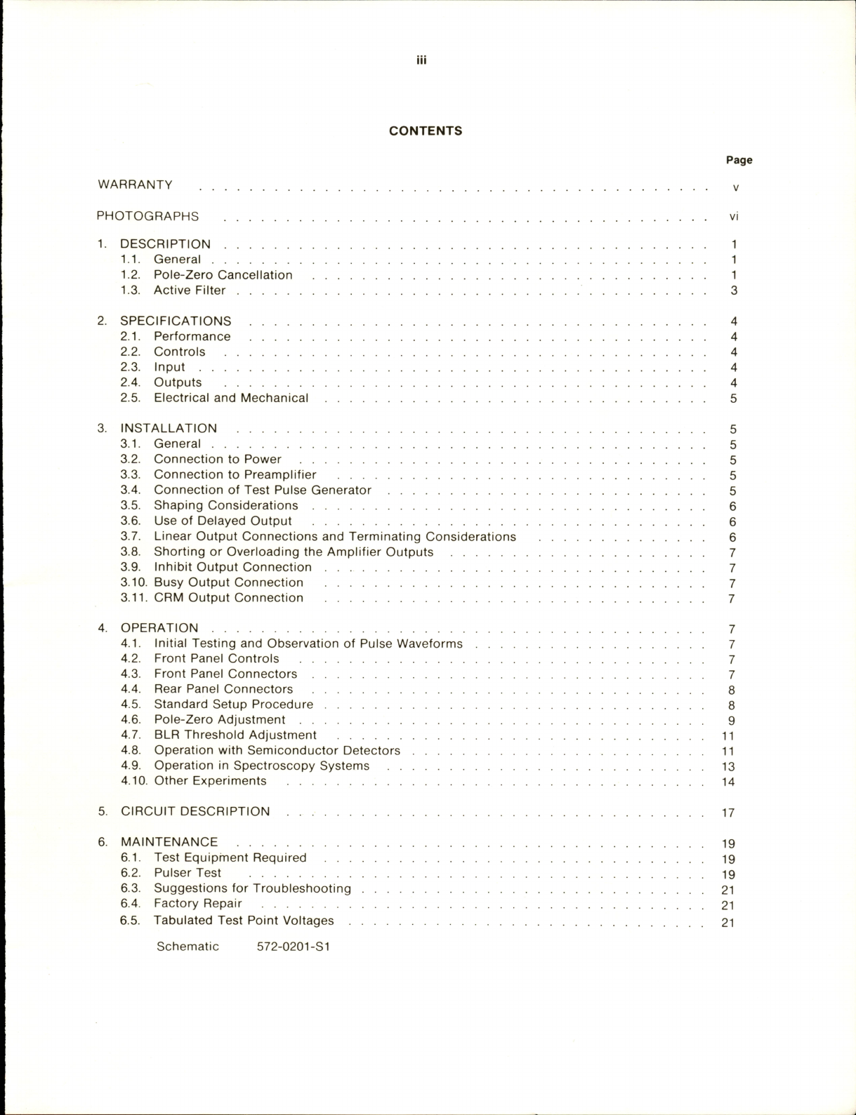
Ill
CONTENTS
WARRANTY
PHOTOGRAPHS
1.
DESCRIPTION
1.1.
General
1.2.
Pole-Zero
Cancellation
1.3.
Active
Filter
Page
V
vi
1
1
1
3
2.
SPECIFICATIONS
2.1.
Performance
2.2.
Controls
2.3.
Input
2.4.
Outputs
2.5.
Electrical
and
Mechanical
3.
INSTALLATION
3.1.
General
3.2.
Connection
to
Power
3.3.
Connection
to
Preamplifier
3.4.
Connection
of
Test
Pulse
Generator
3.5.
Shaping
Considerations
3.6.
Use
of
Delayed
Output
3.7.
Linear
Output
Connections
and
Terminating
Considerations
3.8.
Shorting
or
Overloading
the
Amplifier
Outputs
3.9.
Inhibit
Output
Connection
3.10.
Busy
Output
Connection
3.11.
CRM
Output
Connection
4
4
4
4
4
5
5
5
5
5
5
6
6
6
4.
OPERATION
4.1.
Initial
Testing
and
Observation
of
Pulse
Waveforms
4.2.
Front
Panel
Controls
4.3.
Front
Panel
Connectors
4.4.
Rear
Panel
Connectors
8
4.5.
Standard
Setup
Procedure
8
4.6.
Pole-Zero
Adjustment
9
4.7.
BLR
Threshold
Adjustment
11
4.8.
Operation
with
Semiconductor
Detectors
11
4.9.
Operation
in
Spectroscopy
Systems
13
4.10.
Other
Experiments
14
5.
CIRCUIT
DESCRIPTION
17
6.
MAINTENANCE
19
6.1.
Test
Equipment
Required
19
6.2.
Pulser
Test
19
6.3.
Suggestions
for
Troubleshooting
21
6.4.
Factory
Repair
21
6.5.
Tabulated
Test
Point
Voltages
21
Schematic
572-0201-SI

IV
ILLUSTRATIONS
Fig.
1.1.
Differentiation
in
an
Amplifier
Without
Pole-Zero
Cancellation
2
Fig.
1.2.
Differentiation
in
a
Pole-Zero-Cancelled
Amplifier
2
Fig.
1.3.
Pulse
Shapes
for
Good
Signal-to-Noise
Ratios
3
Fig.
4.1.
Typical
Effects
of
Shaping-Time
Selection
on
Output
Waveforms
8
Fig.
4.2.
Typical
Waveforms
Illustrating
Pole-Zero
Adjustment
Effects;
Oscilloscope
9
Fig.
4.3.
A
Clamp
Circuit
that
Can
Be
Used
to
Prevent
Overloading
the
Oscilloscope
Input
. .
.
.
10
Fig.
4.4.
Pole-Zero
Adjustment
Using
a
Square
Wave
Input
to
the
Preamplifier
10
Fig.
4.5.
BLR
Threshold
Variable
Control
Settings
11
Fig.
4.6.
System
for
Measuring
Amplifier
and
Detector
Noise
Resolution
12
Fig.
4.7.
Noise
as
a
Function
of
Bias
Voltage
12
Fig.
4.8.
System
for
Measuring
Resolution
with
a
Pulse
Height
Analyzer
12
Fig.
4.9.
System
for
Detector
Current
and
Voltage
Measurements
13
Fig.
4.10.
Silicon
Detector
Back
Current
vs
Bias
Voltage
13
Fig.
4.11.
System
for
High-Resolution
Alpha-Particle
Spectroscopy
14
Fig.
4.12.
System
for
High-Resolution
Gamma
Spectroscopy
14
Fig.
4.13.
Scintillation-Counter
Gamma
Spectroscopy
System
14
Fig.
4.14.
High-Resolution
X-Ray
Energy
Analysis
System
Using
a
Proportional
Counter
15
Fig.
4.15.
General
System
Arrangement
for
Gating
Control
15
Fig.
4.16.
Gamma-Ray
Charged-Particle
Coincidence
Experiment
16
Fig.
4.17.
Gamma-Ray
Pair
Spectrometry
16
Fig.
4.18.
Gamma-Gamma
Coincidence
Experiment
17
Fig.
5.1.
Amplifier
Block
Diagram
18
Fig.
5.2.
Timing
Relations
in
the
572
Amplifier
and
Pile-Up
Rejector
19
Fig.
6.1.
Circuit
Used
to
Measure
Nonlinearity
20
STANDARD
WARRANTY
FOR
EG&G
ORTEC
INSTRUMENTS
EG&G
ORTEC
warrants
that
the
items
will
be
delivered
free
from
defects
in
material
or
workmanship.
EG&G
ORTEC
makes
no
other
warranties,
express
or
implied,
and
specifically
NO
WARRANTY
OF
MERCHANTABILITY
OR
FITNESS
FOR
A
PARTICULAR
PURPOSE.
EG&G
ORTEC's
exclusive
liability
is
limited
to
repairing
or
replacing
at
EG&G
ORTEC's
option,
items
found
by
EG&G
ORTEC
to
be
defective
in
workmanship
or
materials
within
one
year
from
the
date
of
delivery.
EG&G
ORTEC's
liability
on
any
claim
of
any
kind,
including
negligence,
loss
or
damages
arising
out
of,
connected
with,
or
from
the
performance
or
breach
thereof,
or
from
the
manufacture,
sale,
delivery,
resale,
repair,
or
use
of
any
item
or
services
covered
by
this
agree
ment
or
purchase
order,
shall
in
no
case
exceed
the
price
allocable
to
the
item
or
service
furnished
or
any
part
thereof
that
gives
rise
to
the
claim.
In
the
event
EG&G
ORTEC
fails
to
manufacture
or
deliver
items
called
for
in
this
agreement
or
purchase
order,
EG&G
ORTEC's
exclusive
liability
and
buyer's
exclusive
remedy
shall
be
release
of
the
buyer
from
the
obligation
to
pay
the
purchase
price.
In
no
event
shall
EG&G
ORTEC
be
liable
for
special
or
consequential
damages.
QUALITY
CONTROL
Before
being
approved
for
shipment,
each
EG&G
ORTEC
instrument
must
pass
a
stringent
set
of
quality
control
tests
designed
to
expose
any
flaws
in
materials
or
workmanship.
Permanent
records
of
these
tests
are
maintained
for
use
in
warranty
repair
and
as
a
source
of
statistical
information
for
design
improvements.
REPAIR
SERVICE
If
it
becomes
necessary
to
return
this
instrument
for
repair,
it
is
essential
that
Customer
Services
be
contacted
in
advance
of
its
return
so
that
a
Return
Authorization
Number
can
be
assigned
to
the
unit.
Also,
EG&G
ORTEC
must
be
informed,
either
in
writing
or
by
telephone
[(615)
482-4411],
of
the
nature
of
the
fault
of
the
instrument
being
returned
and
of
the
model,
serial,
and
revision
("Rev"
on
rear
panel)
numbers.
Failure
to
do
so
may
cause
unnecessary
delays
in
getting
the
unit
repaired.
The
EG&G
ORTEC
standard
procedure
requires
that
instruments
returned
for
repair
pass
the
same
quality
control
tests
that
are
used
for
new-production
instruments.
Instruments
that
are
returned
should
be
packed
so
that
they
will
withstand
normal
transit
handling
and
must
be
shipped
PREPAID
via
Air
Parcel
Post
or
United
Parcel
Service
to
the
nearest
EG&G
ORTEC
repair
center.
The
address
label
and
the
package
should
include
the
Return
Authorization
Number
assigned.
Instruments
being
returned
that
are
damaged
in
transit
due
to
inadequate
packing
will
be
repaired
at
the
sender's
expense,
and
it
will
be
the
sender's
responsibility
to
make
claim
with
the
shipper.
Instruments
not
in
warranty
will
be
repaired
at
the
standard
charge
unless
they
have
been
grossly
misused
or
mishandled,
in
which
case
the
user
will
be
notified
prior
to
the
repair
being
done.
A
quotation
will
be
sent
with
the
notification.
DAMAGE
IN
TRANSIT
Shipments
should
be
examined
immediately
upon
receipt
for
evidence
of
external
or
concealed
damage.
The
carrier
making
delivery
should
be
notified
immediately
of
any
such
damage,
since
the
carrier
is
normally
liable
for
damage
in
shipment.
Packing
materials,
waybills,
and
other
such
documentation
should
be
preserved
in
order
to
establish
claims.
After
such
notification
to
the
carrier,
please
notify
EG&G
ORTEC
of
the
circumstances
so
that
assistance
can
be
provided
in
making
damage
claims
and
in
providing
replacement
equipment
if
necessary.
VI
•
A.
*
•
'
v^..",
■
(j
.'V'V'
■ ■
■■■
-j
:.;
>!•
;■•'
■-.-
•1.4
.
,
-
?
V:"
-
T>
y;
ifj-^
AMPLIFIER
COflRSb
GRIN
100
200
50
• •
500
\.
'
0
♦
IK
SHAPING
TIME
(jjisec)
2
3
1
*
/
6
N
;
^
S
«
10
:s^b..-:-
■■
s«
i
■'■
iN
!NH'
i
i-OUTPUTS
_
iHjNI
CRM'
lil
BUSY
!
J
I'UFAMP
^ma
•!!^&
•3«&
••••t
9*#
sS:':
iji^

ORTEC
572
SPECTROSCOPY
AMPLIFIER
AND
PILE-UP
REJECTOR
1.
DESCRIPTION
1.1.
GENERAL
The
ORTEC
572
Spectroscopy
Amplifier
and
Pile-Up
Rejector
is
a
single-width
NIM
module
with
a
versatile
combination
of
switch-selectable
pulse-shaping
and
out
put
characteristics.
It
features
extremely
low
noise,
wide
gain
range,
and
excellent
overload
response
for
universal
application
in
high-resolution
spectroscopy.
It
accepts
input
pulses
of
either
polarity
that
originate
in
germanium
or
silicon
semiconductor
detectors,
in
scintillation
counters
with
either
fast
or
slow
scintillators,
in
propor
tional
counters,
in
pulsed
ionization
chambers,
in
elec
tron
multipliers,
etc.
The
572
has
an
input
impedance
of
approximately
500fl
and
accepts
either
positive
or
negative
input
pulses
with
rise
times
<650
ns
and
fall
times
>40
fis.
Six
integrate
and
differentiate
time
constants
are
switch-selectable
to
pro
vide
optimum
shaping
for
resolution
and
count
rate.
The
first
differentiation
network
has
variable
pole-zero
can
cellation
that
can
be
adjusted
to
match
preamplifiers
with
decay
times
>40
^xs.
The
pole-zero
cancellation
dras
tically
reduces
the
undershoot
after
the
first
differentiator
and
greatly
improves
overload
and
count
rate
charac
teristics.
In
addition,
the
amplifier
contains
an
active
filter
shaping
network
that
optimizes
the
signal-to-noise
ratio
and
minimizes
the
overall
resolving
time.
Both
unipolar
and
bipolar
outputs
are
provided
simultaneously
on
the
front
and
rear
panels.
The
unipolar
output
should
be
used
for
spectroscopy
when
dc
coupling
can
be
maintained
from
the
572
to
the
analyzer.
A
BLR
(baseline
restorer)
circuit
is
included
in
the
572
for
improved
performance
at
all
count
rates.
Baseline
correction
is
applied
during
intervals
between
input
pulses
only
and
a
front
panel
switch
selects
a
discriminator
level
to
identify
input
pulses.
The
unipolar
output
dc
level
can
be
adjusted
in
the
range
from
-lOOmV
to
+100
mV.
This
output
permits
the
use
of
the
direct-
coupled
input
of
the
analyzer
with
a
minimum
amount
of
interface
problems.
The
572
bipolar
output
may
be
preferable
for
spectroscopy
when
operating
into
an
ac-
coupled
system
at
high
counting
rates.
Internal
pulse
pileup
(a
second
pulse
arriving
before
the
first
pulse
has
been
completed)
is
sensed
internally.
The
572
includes
an
Inhibit
output
BNC
connector
on
the
rear
panel
that
can
be
used
to
inhibit
measurement
of
the
result
of
a
pulse
pileup
when
it
occurs.
The
572
can
be
used
for
constant-fraction
timing
when
operated
in
conjunction
with
an
ORTEC
551, 552,
or
553
Timing
Single-Channel
Analyzer.
The
ORTEC
Timing
Single-Channel
Analyzers
feature
a
minimum
of
walk
as
a
function
of
pulse
amplitude
and
incorporate
a
variable
delay
time
on
the
output
pulse
to
enable
the
timing
pickoff
output
to
be
placed
in
time
coincidence
with
other
signals.
A
switch-selectable
2-ns
delay
is
also
provided
on
the
unipolar
output
to
aid
in
obtaining
the
proper
timing
of
the
linear
pulse
in
a
coincidence-gated
system.
The
572
has
complete
provisions,
including
power,
for
operating
any
ORTEC
solid-state
preamplifier.
Normally,
the
preamplifier
pulses
should
have
a
rise
time
of
0.25
yus
or
less
to
properly
match
the
amplifier
filter
network
and
a
decay
time
greater
than
40
ns
for
proper
pole-zero
cancellation.
The
572
input
impedance
is
500n.
When
long
preamplifier
cables
are
used,
the
cables
can
be
terminated
in
series
at
the
preamplifier
end
or
in
shunt
at
the
amplifier
end
with
the
proper
resistors.
The
output
impedance
is
about
0.1
fl
at
the
front
panel
connectors
and
93fl
at
the
rear
panel
connectors.
The
front
panel
outputs
can
be
connected
to
other
equipment
by
a
single
cable
going
to
all
equipment
and
shunt
terminated
at
the
far
end
of
the
cabling.
If
series
termination
is
desired,
the
rear
panel
connectors
can
be
used
to
connect
the
572
to
other
modules.
See
Section
3
for
further
information.
1.2.
POLE-ZERO
CANCELLATION
Pole-zero
cancellation
is
a
method
for
eliminating
pulse
undershoot
after
the
first
differentiating
network.
In
an
amplifier
not
using
pole-zero
cancellation
(Fig.
1.1)
the
exponential
tail
on
the
preamplifier
output
signal
(usually
50
to
500
/us)
causes
an
undershoot
whose
peak
amplitude
is
roughly
determined
from:
undershoot
amplitude
differentiated
pulse
amplitude
differentiation
time
preamplifier
pulse
decay
time
For
a
^-^lS
differentiation
time
and
a
50-mS
pulse
decay
time
the
maximum
undershoot
is
2%,
and
this
decays
with
a
50-^xs
time
constant.
Under
overload
conditions
this
undershoot
is
often
sufficiently
large
to
saturate
the
amplifier
during
a
considerable
portion
of
the
under
shoot,
causing
excessive
dead
time.
This
effect
can
be
reduced
by
increasing
the
preamplifier
pulse
decay
time
(which
generally
reduces
the
counting
rate
capabilities
of
the
preamplifier)
or
compensating
for
the
undershoot
by
using
pole-zero
cancellation.
Pole-zero
cancellation
is
accomplished
by
the
network
shown
in
Fig.
1.2.
The
pole
[s
+
(1/To)]
due
to
the
preamplifier
pulse
decay
time
is
cancelled
by
the
zero
of

Bo
(t)
o(t)
=
Ernax
I
e,
(t)
Undershoot
nk^r^
First
Differentiated
olJtnSt
X
differentiation
=
pulse
output
A
undersfioot
^max
X
G(t)
=
e,(t).
1
s
X
=
Ei(s)
(Laplace
transform).
■
max
1
1
s
+
—
s
+
7"
o
Rj
Ci
200409
-r
To
e-f/^o
_
7",
e-f/7"o
=
g,
(t),
where
r,
=
R,
C,
10
-
'
\
Fig.
1.1.
Differentiation
in
an
Ampiifier
Without
Poie-Zero
Canceilation.
0
<Ar<i
Bo
(t)
^rnax
b
^
Bi
(t)
No
Undershoot
Pole-zero
Differentiated
Charge
loop
w
cancelled
_
pulse
output
differentiation
without
network
undershoot
Pole
zero
cancel
by
letting
1
K
s
+
—
=
s
+
■
T
o
RzCi
£"max
X
G(t)
=e,(t)
.
s
+
_!_,
Rzc.
k.
mav
.•
^
"lax
1
"
R
,
+
Rj
'""To
^""R.RzC,
E\
(s),
(Laplace
transform).
-max
r^max
RI
-r
Rt
s
+
_
_
_
s
+
R
:j
=
£
I
(sj,
where
Rp
=
R.Rz
R,
+
Rj
I
RzC]
RpCi
p
Q
f/Rp^l
-
P,
/ti
r^max
"
-
ci
ii;
.
200410
Fig.
1.2.
Differentiation
in
a
Pole-Zero
Canceiied
Amplifier.
the
network
[s
+
(K/R2C1)].
In
effect,
the
do
path
across
the
differentiation
capacitor
adds
an
attenuated
replica
of
the
preamplifier
pulse
to
just
cancel
the
negative
under
shoot
of
the
differentiating
network.
Total
preamplifier-amplifier
pole-zero
cancellation
re
quires
that
the
preamplifier
output
pulse
decay
time
be
a
single
exponential
decay
and
matched
to
the
pole-zero
cancellation
network.
The
variable
pole-zero
cancellation
network
allows
accurate
cancellation
for
all
preamplifiers
having
40-^8
or
greater
decay
times.
Improper
matching
of
the
pole-zero
network
will
degrade
the
overload
perfor
mance
and
cause
excessive
pileup
distortion
at
medium
counting
rates.
Improper
matching
causes
either
an
undercompensation
(undershoot
is
not
eliminated)
or
an
overcompensation
(output
after
the
main
pulse
does
not
return
to
the
baseline
but
decays
to
the
baseline
with
the
preamplifier
time
constant).
The
pole-zero
adjust
is
accessible
on
the
front
panel
of
the
572
and
can
easily
be
adjusted
by
observing
the
baseline
on
an
oscilloscope
with
a
monoenergetic
source
or
pulser
having
the
same
decay
time
as
the
preamplifier
under
overload
conditions.
The
adjustment
should
be
made
so
that
the
pulse
returns
to
the
baseline
in
the
minimum
time
with
no
undershoot.
1.3.
ACTIVE
FILTER
When
only
FET
gate
current
and
drain
thermal
noise
are
considered,
the
best
signal-to-noise
ratio
occurs
when
the
two
noise
contributions
are
equal
for
a
given
input
pulse
shape.
The
Gaussian
pulse
shape
(Fig.
1.3)
for
this
condition
requires
an
amplifier
with
a
single
RC
differen
tiate
and
n
equal
RC
integrates
where
n
approaches
in
finity.
The
Laplace
transform
of
this
transfer
function
is
G(s)
=
1
s
+
(1/RC)
[s
+
(1/RC)]"
(n
-
=0).
where
the
first
factor
is
the
single
differentiate
and
the
second
factor
is
the
n
integrates.
The
572
active
filter
approximates
this
transfer
function.
Figure
1.3
illustrates
the
results
of
pulse
shaping
in
an
amplifier.
Of
the
four
pulse
shapes
shown
the
cusp
would
produce
minimum
noise
but
is
impractical
to
achieve
with
normal
electronic
circuitry
and
would
be
difficult
to
measure
with
an
ADC.
The
true
Gaussian
shape
deteriorates
the
signal-to-noise
ratio
by
only
about
12%
from
that
of
the
cusp
and
produces
a
signal
that
is
easy
to
measure,
but
requires
many
sections
of
integration
(n
—
00).
With
two
sections
of
integration
the
waveform
identified
as
a
Gaussian
approximation
can
be
obtained,
and
this
deteriorates
the
signal-to-noise
ratio
by
about
22%.
The
ORTEC
active
filter
network
in
the
572
Amplifier
provides
the
fourth
waveform
in
Fig.
1.3;
this
waveform
has
characteristics
superior
to
the
Gaussian
approxima
tion,
yet
obtains
them
with
four
complex
poles.
By
this
method
the
output
pulse
shape
has
a
good
signal-to-
noise
ratio,
is
easy
to
measure,
and
yet
requires
only
a
Ralative
Noise
CUSP
I/RC
GAUSSIAN
1.12
1
s
+
(imC)
ls
+
(1/RCIl"
1.22
GAUSSIAN
APPROXIMATION
FOR
n
-
2
(1/RCI
U
+
(1/RC))'
ACTIVE
FILTER
-1.17
(s
+
(1/RC)1
1
[s
+
(3/RC)l
[s
+
(1
-
kj)/RCl
Is
+
(1
+
kj)/RCl
j
=
k
=
0.3
Fig.
1.3.
Puise
Shapes
for
Good
Signal-to-Noise
Ratios.
practical
amount
of
electronic
circuitry
to
achieve
the
desired
results.
2.
SPECIFICATIONS
2.1.
PERFORMANCE
GAIN
RANGE
Continuously
adjustable
from
XI
through
X1500.
PULSE
SHAPING
Gaussian
on
all
ranges
with
peaking
time
equal
to
2.2r
and
pulse
width
at
0.1%
level
equal
to
2.9
times
the
peaking
time.
INTEGRAL
NONLINEARITY
<0.05%
(0.025%
typical)
using
2
^is
shaping.
NOISE
<8
/jV
referred
to
the
input
(5
typical)
using
2
MS
shaping
and
gain
^100.
TEMPERATURE
INSTABILITY
Gain
<0.0075%/°
0,
0
to
50°
C.
DC
Level
<±50
mV/°G,
0
to
50°C.
CROSSOVER
WALK
<±3
ns
for
50:1
dynamic
range,
including
contribution
of
ORTEG
551
or
552
Constant-
Fraction
Timing
Single-Channel
Analyzer
using
50%
fraction
and
0.5
fxs
shaping.
COUNT
RATE
STABILITY
The
1.33
MeV
gamma
ray
peak
from
a
"'Co
source,
positioned
at
85%
of
analyzer
range,
typically
shifts
<0.024%,
and
its
FWHM
broadens
<16%
when
its
incoming
count
rate
changes
from
0
to
100
000
counts/s
using
2
ms
shaping.
The
amplifier
will
hold
the
baseline
reference
up
to
count
rates
in
excess
of
150
000
counts/s.
OVERLOAD
RECOVERY
Recovers
to
within
2%
of
rated
output
from
X300
overload
in
2.5
nonoverloaded
unipolar
pulse
widths,
using
maximum
gain;
same
recovery
from
XI000
overload
for
bipolar
pulses.
2.2.
CONTROLS
GAIN
Ten-turn
precision
potentiometer
for
continu
ously
variable
direct-reading
gain
factor
of
X0.5
to
XI.5.
COARSE
GAIN
Six-position
selector
switch
selects
feedback
resistors
for
gain
factors
of
20,
50,100,200,500,
and
IK.
INPUT
ATTENUATOR
Jumper
on
printed
circuit
board
selects
an
input
attenuation
factor
of
1
or
10
(gain
factor
of
XI
or
X0.1).
POS/NEG
Toggle
switch
selects
input
circuit
for
either
polarity
of
input
pulses
from
the
preamplifier.
SHAPING
TIME
Six-position
switch
selects
time
con
stant
for
active
filter
network
pulse
shaping;
selections
are
0.5,
1,
2,
3,
6,
and
10
ms.
PZ
ADJ
Potentiometer
to
adjust
pole-zero
cancellation
for
decay
times
from
40
tis
to
°o.
Factory
preset
at
50
ns
to
match
normal
characteristics
of
ORTEC
preamplifiers.
BLR
Toggle
switch
selects
a
source
for
the
gated
baseline
restorer
discriminator
threshold
level
from
one
of
three
positions.
Auto
The
BLR
threshold
is
automatically
set
to
an
optimum
level
as
a
function
of
the
signal
noise
level
by
an
internal
circuit.
This
allows
easy
setup
and
very
good
performance
under
most
conditions.
PZ
Ad]
The
BLR
threshold
is
determined
by
the
thresh
old
potentiometer.
The
BLR
time
constant
is
greatly
In
creased
to
facilitate
PZ
adjustment.
This
position
may
give
the
lowest
noise
for
conditions
of
low
count
rate
and/or
longer
shaping
times.
Threshold
The
BLR
threshold
Is
set
manually
by
the
threshold
potentiometer.
Range
is
0
to
300
mV
referred
to
the
positive
output
signal.
The
BLR
time
constant
is
the
same
as
for
the
Auto
switch
setting.
DC
Screwdriver
potentiometer
adjusts
the
unipolar
output
baseline
dc
level;
range,
+100
mV
to
-100
mV.
DELAY/OUT
Toggle
switch
selects
either
2
ms
delay
(Delay)
or
prompt
(Out)
timing
for
the
unipolar
output.
2.3.
INPUT
INPUT
Type
BNC
front
and
rear
panel
connectors
accept
either
positive
or
negative
pulses
with
rise
times
in
the
range
from
10
to
650
ns
and
decay
times
from
40
to
2000
fis:
Z,„
~500n,
dc
coupled;
linear
maximum,
1
V
(10
V
with
attenuator
jumper
set
at
X0.1);
absolute
maximum,
20
V.
2.4.
OUTPUTS
UNI
Unipolar
front
panel
BNC
with
Z„
<111
and
rear
panel
BNC
with
Z„
=
93n.
Short-circuit
proof;
prompt
or
delayed,
full
scale
linear
range
0
to
+10
V;
active
filter
shaped
and
dc
restored;
dc
level
adjustable
to
±100
mV.
Bl
Bipolar
front
panel
BNC
with
Z„
<1
n
and
rear
panel
BNC
with
Z„
=
9311.
Short-circuit
proof;
prompt
output
with
positive
lobe
leading
and
linear
range
of
±10
V;
active
filter
shaped.
BUSY
Rear
panel
BNC
with
Z„
<10n
provides
a
+5
V
logic
pulse
for
the
duration
that
the
input
pulse
exceeds
the
baseline
restorer
discriminator
level.
Connect
to
the
ORTEC
MCA
Busy
input
for
dead
time
correction.
INH
Inhibit
rear
panel
BNC
with
Z„
<10n
provides
a
nominal
+5
V
logic
signal
when
an
internal
pulse
pileup
occurs;
width
~6r
in
coincidence
with
the
pileup;
to
be
used
for
an
MCA
anticoincidence
input
to
prevent
storage
of
pileup
data
in
the
spectrum.
CRM
Count
Ratemeter
rear
panel
BNC
furnishes
a
nominal
+5
V
logic
signal
for
every
linear
input
pulse;
width,
500
ns;
to
be
used
as
an
input
to
a
ratemeter
or
counter.
PREAMP
POWER
Rear
panel
standard
ORTEC
power
connector;
Amphenol
17-10090;
mates
with
captive
and
non-captive
power
cords
on
all
standard
ORTEC
preamplifiers.
2.5.
ELECTRICAL
AND
MECHANICAL
POWER
REQUIRED
(not
Including
any
load
on
the
Preamp
Power
connector)
+24
V,
100
mA;
-24
V,
105
mA;
+12
V,
85
mA;-12
V,
50
mA.
FRONT
PANEL
DIMENSIONS
NIM-standard
single-
width
module
(1.35
by
8.714
in.)
per
TID-20893.
3.
INSTALLATION
3.1.
GENERAL
The
572
operates
on
power
that
must
be
furnished
from
a
NIM-standard
bin
and
power
supply
such
as
the
ORTEC
401/402
Series.
The
bin
and
power
supply
is
designed
for
relay
rack
mounting.
If
the
equipment
is
to
be
rack
mounted,
be
sure
that
there
is
adequate
ventilation
to
prevent
any
localized
heating
of
the
components
that
are
used
in
the
572.
The
temperature
of
equipment
mounted
in
racks
can
easily
exceed
the
maximum
limit
of
50°C
unless
precautions
are
taken.
3.2.
CONNECTION
TO
POWER
The
572
contains
no
internal
power
supply
and
must
obtain
the
necessary
dc
operating
power
from
the
bin
and
power
supply
in
which
it
is
installed
for
operation.
Always
turn
off
power
for
the
power
supply
before
inserting
or
removing
any
modules.
After
all
modules
have
been
installed
in
the
bin
and
any
preamplifiers
have
also
been
connected
to
the
Preamp
Power
connectors
on
the
amplifiers,
check
the
dc
voltage
levels
from
the
power
supply
to
see
that
they
are
not
overloaded.
The
ORTEC
401/402
Series
Bins
and
Power
Supplies
have
convenient
test
points
on
the
power
supply
control
panel
to
permit
monitoring
these
dc
levels.
If
any
one
or
more
of
the
dc
levels
indicates
an
overload,
some
of
the
modules
will
need
to
be
moved
to
another
bin
to
achieve
operation.
3.3.
CONNECTION
TO
PREAMPLIFIER
The
preamplifier
output
signal
is
connected
to
the
572
through
the
appropriate
Input
BNG
connector
on
the
front
or
rear
panel.
The
input
impedance
is
about
500il
and
is
dc-coupled
to
ground;
therefore
the
preamplifier
output
must
be
either
ac-coupled
or
have
approximately
zero
dc
voltage
under
no-signal
conditions.
The
572
incorporates
pole-zero
cancellation
in
order
to
enhance
the
overload
and
count
rate
characteristics
of
the
amplifier.
This
technique
requires
matching
the
network
to
the
preamplifier
decay
time
constant
in
order
to
achieve
perfect
compensation.
The
pole-zero
adjustment
should
be
set
each
time
the
preamplifier
or
the
shaping
time
constant
of
the
amplifier
is
changed.
For
details
of
the
pole-zero
adjustment
see
Section
4.6.
An
alternate
method
is
accomplished
easily
by
using
a
monoenergetic
source
and
observing
the
amplifier
baseline
with
an
oscilloscope
after
each
pulse
under
approximately
X2
overload
conditions.
Adjustment
should
be
made
so
that
the
pulse
returns
to
the
baseline
in
a
minimum
amount
of
time
with
no
undershoot.
Preamplifier
power
at
+24
V,
-24
V,
+12
V,
and
-12
V
is
available
through
the
Preamp
Power
connector
on
the
rear
panel.
When
the
preamplifier
is
connected,
its
power
requirements
are
obtained
from
the
same
bin
and
power
supply
as
is
used
for
the
amplifier,
and
this
increases
the
dc
loading
on
each
voltage
level
over
and
above
the
requirements
for
the
572
at
the
module
position
in
the
bin.
When
the
572
is
used
with
a
remotely
located
preamplifier
(i.e.,
preamplifier-to-amplifier
connection
through
25
ft
or
more
of
coaxial
cable),
be
careful
to
ensure
that
the
characteristic
impedance
of
the
transmission
line
from
the
preamplifier
output
to
the
572
input
is
matched.
Since
the
input
impedance
of
the
572
is
about
500il,
sending-
end
termination
wil
l
normally
be
preferred;
the
transmission
line
should
be
series-terminated
at
the
preamplifier
output.
All
ORTEC
preamplifiers
contain
series
terminations
that
are
either
93fl
or
variable;
coaxial
cable
type
RG-62/U
or
RG-71/U
is
recommended.
3.4.
CONNECTION
OF
TEST
PULSE
GENERATOR
THROUGH
A
PREAMPLIFIER
The
satisfactory
connection
of
a
test
pulse
generator
such
as
the
ORTEC
419
Precision
Pulse
Generator
or
equivalent
depends
primarily
on
two
considerations;
the
preamplifier
must
be
properly
connected
to
the
572
as
discussed
in
Section
3.3,
and
the
proper
input
signal
simulation
must
be
applied
to
the
preamplifier.
To
ensure
proper
input
signal
simula
tion,
refer
to
the
instruction
manual
for
the
particular
pre
amplifier
being
used.
DIRECTLY
INTO
THE
572
Since
the
input
of
the
572
has
500(1
of
input
impedance,
the
test
pulse
generator
will
normally
have
to
be
terminated
at
the
amplifier
input
with
an
additional
shunt
resistor.
In
addition,
if
the
test
pulse
generator
has
a
dc
offset,
a
large
series
Isolating
capacitor
is
also
required
since
the
572
input
is
dc
coupled.
The
ORTEC
test
pulse
generators
are
designed
for
direct
connection.
When
any
one
of
these
units
is
used,
it
should
be
terminated
with
a
lOOn
terminator
at
the
amplifier
input
or
be
used
with
at
least
one
of
the
output
attenuators
set
at
In.
(Thesmall
errorduetothefinite
input
impedance
of
the
amplifier
can
normally
be
neglected.)
SPECIAL
CONSIDERATIONS
FOR
POLE-ZERO
CANCELLATION
When
a
tail
pulser
is
connected
directly
to
the
amplifier
input,
the
PZ
Adj
should
be
adjusted
if
overload
tests
are
to
be
made
(other
tests
are
not
affected).
See
Section
4.6
for
the
pole-zero
adjustment.
If
a
preamplifier
is
used
and
a
tail
pulser
is
connected
to
the
preampl
ifier
test
input,
similar
precautions
are
necessary.
In
this
case
the
effect
of
the
pulser
decay
must
be
removed;
i.e.,
astep
input
should
be
simulated.
3.5.
SHAPING
CONSIDERATIONS
The
shaping
time
constant
on
the
572
is
switch-selectable
in
steps
of
0.5,
1,
2,
3,
6,
and
10
ns.
The
choice
of
the
proper
shaping
time
constant
is
generally
a
compromise
between
operating
at
a
shorter
time
constant
for
accommodation
of
high
counting
rates
and
operating
with
a
longer
time
constant
for
a
better
signal-to-noise
ratio.
For
scintillation
counters
the
energy
resolution
depends
largely
on
the
scintillator
and
photomultiplier,
and
therefore
a
shaping
time
constant
of
about
fourtimes
the
decay-time
constant
of
the
scintillator
is
a
reasonable
choice
(for
Nal,
a
1-;us
shaping
time
constant
is
about
optimum).
For
gas
proportional
counters
the
collection
time
is
normally
in
the
0.5
to
5
/us
range
and
a
2
/is
or
greater
time
constant
selection
will
generally
give
optimum
resolution.
For
surface
barrier
semiconductor
detectors,
a
0.5
to
2
resolving
time
will
generally
provide
optimum
resolution.
Shaping
time
for
Ge(Li)
detectors
will
vary
from
1
to
6
/us,
depending
on
the
size,
configuration,
and
collection
time
of
the
specific
detector
and
preamplifier.
When
a
charge-sensitive
preamplifier
is
used,
the
optimum
shaping
time
constant
to
minimize
the
noise
of
a
system
can
be
determined
by
measuring
the
output
noise
of
the
system
and
dividing
it
by
the
system
gain.
Since
the
572
has
almost
constant
gain
for
all
shaping
modes,
the
optimum
shaping
can
be
determined
by
measuring
the
output
noise
of
the
572
with
a
voltmeter
as
each
shaping
time
constant
is
selected.
The
572
provides
both
unipolar
and
bipolar
outputs.
The
unipolar
output
pulses
should
be
used
in
applications
where
the
best
signal-to-noise
ratio
(resolution)
is
most
important,
such
as
high-resolution
spectroscopy
using
semiconductor
detectors.
Use
of
the
unipolar
output
with
baseline
restoration
will
also
give
excellent
resolution
at
high
counting
rates.
The
bipolar
output
should
be
used
in
high
count
rate
systems
when
the
analyzer
system
is
ac-
coupled
and
noise,
or
resolution,
is
a
secondary
consideration.
3.6.
USE
OF
DELAYED
OUTPUT
The
unipolar
output
can
be
either
prompt
or
delayed.
The
prompt
output
is
used
for
normal
spectroscopy
applica
tions.
The
delayed
output
(equal
in
amplitude
to
the
prompt
output
but
delayed
by
2
;^s)
is
used
in
coincidence
experiments
where
the
delay
can
compensate
for
time
delays
in
obtaining
the
coincidence
information.
The
considerations
regarding
the
proper
choice
of
shaping
time
for
the
delayed
output
are
discussed
in
Section
3.5.
3.7.
LINEAR
OUTPUT
CONNECTIONS
AND
TERMINATING
CONSIDERATIONS
Since
the
572
unipolar
output
is
normally
used
for
spectroscopy
the
572
is
designed
with
a
great
amount
of
flexibility
in
order
for
the
pulse
to
be
interfaced
with
an
analyzer.
A
gated
baseline
restorer
(BLR)
circuit
is
included
in
this
output
for
improved
performance
at
all
count
rates.
A
switch
on
the
front
panel
permits
the
threshold
for
the
restorer
gate
to
be
determined
automatically,
according
to
the
input
noise
level,
or
manually,
with
a
screwdriver
adjustment.
The
switch
also
has
a
center
PZ
Adj
setting
that
can
be
used
to
eliminate
the
BLR
effect
when
making
pole-zero
adjustments.
The
unipolar
output
dc
level
can
be
adjusted
from
-0.1
to
+0.1
V
to
set
the
zero
intercept
on
the
analyzer
when
direct
coupling
is
used.
The
bipolar
output,
with
a
0
to
10
V
range,
can
be
used
for
crossover
timing
or
may
be
preferred
for
spectroscopy
when
operating
into
ac-
coupled
systems
at
high
counting
rates.
Typical
system
block
diagrams
for
a
variety
of
experiments
are
described
in
Section
4.
Three
general
methods
of
termination
are
used.
The
simplest
of
these
is
shunt
termination
at
the
receiving
end
of
the
cable.
A
second
method
is
series
termination
at
the
sending
end.
The
third
is
a
combination
of
series
and
shunt
termination,
where
thecable
impedance
is
matched
both
in
series
at
the
sending
end
and
in
shunt
at
the
receiving
end.
The
combination
is
most
effective,
but
this
reduces
the
amount
of
signal
strength
at
the
receiving
end
to
50%
of
that
which
is
available
in
the
sending
instrument.
To
use
shunt
termination
at
the
receiving
end
of
thecable,
connect
the
<1fl
output
of
the
572
(on
the
front
panel)
through
93fl
cable
to
the
input
of
the
receiving
instru
ment.
Then
use
a
BNC
tee
connector
to
attach
both
the
interconnecting
cable
and
a
100(1
terminator
at
the
input
connector
of
the
receiving
instrument.
Since
the
input
impedance
of
the
receiving
instrument
is
normally
1000(1
or
more,
the
effective
instrument
input
impedance
with
the
100(1
terminator
will
be
of
the
order
of
93(1
and
this
matches
the
cable
impedance
correctly.
For
series
termination
use
the
93(1
output
of
the
572
for
the
cable
connection.
Use
93(1
cable
to
interconnect
this
into
the
input
of
the
receiving
instrument.
The
1000(1
(or
more)
normal
input
impedance
at
the
input
connector
represents
an
essentially
open
circuit,
and
the
series
impedance
in
the
572
now
provides
the
proper
termina
tion
for
the
cable.
For
the
combination
of
series
and
shunt
termination,
use
the
93il
output
on
the
rear
panel
of
the
572
and
use
931t
cable.
At
the
input
for
the
receiving
instrument
use
a
BNC
tee
to
attach
both
the
signal
cable
and
a
lOOfl
resistive
terminator.
Note
that
the
signal
span
at
the
receiving
end
of
this
type
of
circuit
will
always
be
reduced
to
50%
of
the
signal
span
furnished
by
the
sending
instrument.
For
customer
convenience,
ORTEC
stocks
the
proper
terminators
and
BNC
tees,
or
they
can
be
ordered
from
a
variety
of
commercial
sources.
3.8.
SHORTING
OR
OVERLOADING
THE
AMPLIFIER
OUTPUTS
All
outputs
of
the
572
are
dc-coupled
with
an
output
im
pedance
of
about
0.1
II
for
the
front
panel
connectors
and
9311
for
the
rear
panel
connectors.
If
the
output
is
shorted
with
a
direct
short
circuit
the
output
stage
will
limit
the
peak
current
of
the
output
so
that
the
amplifier
will
not
be
harmed.
When
the
amplifier
is
terminated
with
10011,
the
maximum
rate
allowed
to
maintain
the
linear
output
is
[200
000
cps/r(MS)]
X
[10/V.,(V)].
3.9.
INHIBIT
OUTPUT
CONNECTION
The
Inhibit
output
on
the
rear
panel
is
intended
for
application
at
the
anticoincidence
input
of
the
Analyzer.
An
output
pulse
is
generated
through
this
connector
when
a
pulse
pileup
is
sensed
in
the
572,
and
the
pulse
can
then
be
used
to
prevent
the
Analyzer
from
measuring
and
storing
a
false
amplitude.
The
signal
is
dc-coupled
and
rises
from
0
to
about
+5
V
for
a
time
equal
to
6r,
starting
when
a
pileup
occurs.
3.10.
BUSY
OUTPUT
CONNECTION
The
signal
through
the
rear
panel
Busy
output
connector
rises
from
0
to
about
+5
V
at
the
onset
of
each
linear
input
pulse.
Its
width
is
equal
to
the
time
the
input
pulse
amplitude
exceeds
the
BLR
discriminator
level,
and
is
extended
automatically
by
the
generation
of
an
Inhibit
output
signal.
It
can
be
used
to
provide
MCA
live-time
correction,
to
control
the
generation
of
input
pulses,
to
observe
normal
operation
with
an
oscilloscope,
orforany
of
a
variety
of
other
applications.
Its
use
is
optional
and
no
termination
is
required
if
the
output
is
not
being
used.
3.11.
CRM
OUTPUT
CONNECTION
One
NIM-standard
positive
logic
pulse
is
generated
to
correspond
to
each
linear
input
pulse
into
the
572.
The
pulses
are
available
through
the
CRM
(Count
Rate
Meter)
output
BNC
on
the
rear
panel
and
are
intended
for
use
in
a
count
rate
meter
or
counter
to
monitor
the
true
input
count
rate
into
the
amplifier.
Its
use
is
optional
and
no
termination
is
required
if
the
output
is
not
being
used.
4.
OPERATION
4.1.
INITIAL
TESTING
AND
OBSERVATION
OF
PULSE
WAVEFORMS
Refer
to
Section
6
for
information
on
testing
performance
and
observing
waveforms
at
front
panel
test
points.
Figure
4.1
shows
some
typical
unipolar
and
bipolar
output
waveforms.
4.2.
FRONT
PANEL
CONTROLS
GAIN
A
coarse
Gain
switch
and
a
Gain
10-turn
locking
precision
potentiometer
select
and
precisely
adjust
the
gain
factor
forthe
amplification
in
the
572.
Switch
settings
are
X20,
50,
100,
200,
500,
and
1000.
Continuous
fine
gain
range
is
from
X0.5
to
XI
.5,
using
markings
of
500
through
1500
dial
divisions.
An
internal
jumper
setting
provides
one
additional
gain
factor
selection
of
either
X1.0
or
X0.1.
Collectively
the
range
of
gain
can
be
set
at
any
level
from
XI.0
through
X1500,
using
all
three
of
these
controls.
POS/NEG
A
toggle
switch
selects
an
input
circuit
that
accepts
either
polarity
of
pulses
from
the
preamplifier.
PZ
ADJ
A
screwdriver
control
to
set
the
pole-zero
cancellation
to
match
the
preamplifier
pulse
decay
characteristics.
The
range
is
from
40
ijls
to
infinity.
DC
A
screwdriver
control
adjusts
the
dc
baseline
level
of
the
unipolar
output
in
the
range
of
-0.1
V
to
+0.1
V.
DELAY
A
toggle
switch
selects
either
prompt
(Out)
or
2
/iS
delay
timing
for
the
unipolar
output
signals.
SHAPING
A
6-position
switch
selects
equal
integrate
and
differentiate
time
constants
to
shape
the
input
pulses.
Settings
are
0.5,
1,
2,
3,
6,
and
10
/us.
BLR
A
3-position
toggle
switch
controls
the
operation
of
the
internal
baseline
restorer
(BLR)
circuit.
The
center
setting
of
the
switch
is
effectively
Off,
and
this
permits
adjustment
of
the
PZ
Adj
control
without
interference
from
the
BLR
circuit.
The
Auto
setting
of
the
switch
selects
a
circuit
that
regulates
the
threshold of
the
BLR
gate
according
to
the
output
noise
level.
The
Threshold
setting
permits
manual
control
of
the
BLR
gate
threshold,
using
the
screwdriver
control
immediately
below
the
toggle
switch.
4.3.
FRONT
PANEL
CONNECTORS
INPUT
Accepts
input
pulses
to
be
shaped
and/or
amplified
by
the
572.
Compatible
characteristics;
positive
or
negative
with
rise
time
from
10
to
650
ns;
decay
time

Shaping
Time
0.5
mS
Shaping
Time
1
us
Shaping
Fig.
4.1.
Typical
Effects
of
Shaping-Time
Seiection
on
Output
Waveforms.
greater
than
40
iis
for
proper
pole-zero
cancellation;
input
linear
amplitude
range
0
to
10
V,
with
a
maximum
limit
of
±20
V.
Input
impedance
is
approximately
500n.
UNI
Provides
a
unipolar
positive
output
with
charac
teristics
that
are
related
to
input
peak
amplitude,
gain,
shaping
time
constants,
pole-zero
cancellation,
and
baseline
stabilization.
The
dc
baseline
level
is
adjustable
for
offset
to
±0.1
V.
Timing
can
be
either
prompt
or
delayed
2
with
respect
to
the
input.
Output
impedance
through
this
connector
is
about
O.in,
dc
coupled.
Linear
range
0
to
±10
V.
Bi
Provides
a
bipolar
pulse
with
positive
lobe
leading
and
with
characteristics
that
are
related
to
input
peak
amplitude,
gain,
and
shaping
time
constants.
Timing
is
prompt
with
respect
to
the
input.
Crossover
walk
of
this
output
is
less
than
3
ns
(see
Specifications).
Output
impedance
through
this
connector
is
about
O.lfl.
Linear
range
of
0
to
±10
V.
4.4.
REAR
PANEL
CONNECTORS
IN
Bridged
with
front
panel
Inputconnectorforoptional
use
as
an
alternate
input
connection
location.
INH
Provides
an
output
signal
to
identify
a
pulse
pileup
in
the
572.
Connect
it
to
the
anticoincidence
input
of
the
multichannel
analyzer
to
inhibit
measurement
and
storage
of
false
amplitudes.
UNI
Provides
a
unipolar
positive
output
with
the
same
characteristics
as
described
for
the
front
panel
Uni
connector;
the
output
impedance
through
this
connector
is
93fl.
81
Provides
a
bipolar
output
with
the
same
charac
teristics
as
described
for
the
front
panel
Bi
connector;
the
output
impedance
through
this
connector
is
93n.
CRM
Provides
a
NIM-standard
(s+5
V)
slow
positive
logic
output
for
each
linear
input
pulse.
The
output
can
be
connected
into
a
ratemeter
or
counter
to
monitor
the
true
input
count
rate
for
the
amplifier.
BUSY
Provides
a
signal
that
rises
to
approximately
±5
V
for
the
time
that
the
input
pulse
amplitude
exceeds
the
BLR
discriminator
level,
which
can
be
controlled
manually
or
automatically.
The
output
can
be
used
to
correct
for
live
time
in
the
ORTEC
MCA
by
connecting
it
to
the
MCA
Busy
input.
PREAMP
Provides
power
connections
from
the
bin
and
power
supply
to
the
ORTEC
preamplifier.
The
dc
levels
include
±24
V,
-24
V,
±12
V,
and
-12
V.
4.5.
STANDARD
SETUP
PROCEDURE
a.
Connect
the
detector,
preamplifier,
high
voltage
power
supply,
and
amplifier
into
a
basic
system
and
con-
net
the
amplifier
unipolar
output
to
an
oscilloscope.
Con
nect
the
preamplifier
power
cable
to
the
Preamp
power
connector
on
the
rear
panel
of
the
572.
Turn
on
power
in

the
Bin
and
Power
Supply
and
allow
the
electronics
of
the
system
to
warm
up
and
stabilize.
b.
Set
the
572
controls
initially
as
follows:
Shaping
Coarse
Gain
Gain
Internal
Jumper
BLR
Thresh
Pos/Neg
2
ns
50
1.000
X1.0
PZ
Adj
Fully
clockwise
Match
preamplifier
output
polarity
c.
Use
a
^°Go
calibration
source,
set
about
25
cm
from
the
active
face
of
the
detector.
The
unipolar
output
pulse
from
the
572
should
be about
8
to
10
V,
using
a
pream
plifier
with
a
conversion
gain
of
170
mV/MeV.
d.
Readjust
the
Gain
control
so
that
the
higher
peak
from
the
^"Co
source
(1.33
MeV)
provides
an
amplifier
output
at
about
9
V.
4.6.
POLE-ZERO
ADJUSTMENT
The
pole-zero
adjustment
is
extremely
critical
for
good
performance
at
high
count
rates.
This
adjustment
should
be
checked
carefully
for
the
best
possible
results.
USING
Ge(Li)
SYSTEM
AND
"Co
a.
Adjust
the
radiation
source
count
rate
between
2
kHz
and
10
kHz.
b.
Observe
the
unipolar
output
with
an
oscilloscope.
Adjust
the
PZ
Adj
control
so
that
the
trailing
edge
of
the
pulses
returns
to
the
baseline
without
overshoot
or
undershoot
(see
Fig.
4.2).
The
oscilloscope
used
must
be
dc-coupled
and
must
not
contribute
distortion
in
the
observed
waveforms.
Oscilloscopes
such
as
Tektronix
453, 454,
465,
and
475
will
overload
for
a
10-V
signal
when
the
vertical
sensitivity
is
less
than
100
mV/cm.
To
prevent
overload
ing
the
oscilloscope,
use
the
clamp
circuit
shown
in
Fig.
4.3.
USING
SQUARE
WAVE
THROUGH
PREAMPLIFIER
TEST
INPUT
A
more
precise
pole-zero
adjustment
in
the
572
can
be
obtained
by
using
a
square
wave
signal
as
the
input
to
the
preamplifier.
Many
oscilloscopes
include
a
calibra
tion
output
on
the
front
panel
and
this
is
a
good
source
of
square
wave
signals
at
a
frequency
of
about
1
kHz.
The
amplifier
differentiates
the
signal
from
the
preamplifier
so
that
it
generates
output
signals
of
alternate
polarities
on
the
leading
and
trailing
edges
of
the
square
wave
input
signal,
and
these
can
be
compared
as
shown
in
Fig.
4.4
to
achieve
excellent
pole-zero
cancellation.
Overcompensated
Adjusted
Properly
Undercompensated
Fig.
4.2.
Typical
Waveforms
Illustrating
Pole-Zero
Adjustment
Effects;
Oscilloscope
Trigger,
572
Busy
Output;
""Co
Source
with
1.33-MeV
Peak
Adjusted
~9
V;
Count
Rate,
3
kHz;
Shaping
Time
Constant,
2

10
FROM
AMPLIFIER
OUTPUT
IK
TO
OSCILLOSCOPE
INPUT
AAA^
D
r
HPA
2800
SCHOTTKY
DIODES
OR
FAST
Ge
DIODES
Fig.
4.3.
A
Clamp
Circuit
ttiat
Can
Be
Used
to
Prevent
Overloading
ttie
Oscilloscope
Input.
Use
the
following
procedure:
a.
Remove
all
radioactive
sources
from
the
vicinity
of
the
detector.
Set
up
the
system
as
for
normal
operation,
including
detector
bias.
b.
Set
the
572
controis
as
for
normal
operation;
this
includes
gain,
shaping,
and
input
polarity.
c.
Connect
the
source
of
1-kHz
square
waves
through
an
attenuator
to
the
Test
input
of
the
preamplifier.
Adjust
the
attenuator
so
that
the
572
output
amplitude
is
about
9
V.
d.
Observe
the
Unipolar
output
of
the
572
with
an
oscilloscope,
triggered
from
the
572
Busy
output.
Adjust
the
PZ
Adj
control
for
proper
response
according
to
Fig.
4.4.
Use
the
clamp
circuit
of
Fig.
4.3
to
prevent
over
loading
the
oscilloscope
input.
Figure
4.4A
shows
the
amplifier
output
as
a
series
of
alternate
positive
and
negative
Gaussian
puises.
In
the
other
three
pictures
of
this
figure
the
oscilloscope
was
triggered
to
show
both
positive
and
negative
pulses
simultaneously.
These
pictures
show
more
detail
to
aid
in
proper
adjustment.
av.
A.
PZ
Properly
Adjusted;
Slow
Trigger
to
Separate
Pulses.
B.
Overcompensated;
Fast
Trigger
to
Superimpose
Pulses.
C.
Properly
Adjusted;
Pulses
Superimposed.
D.
Undercompensated;
Pulses
Superimposed.
Fig.
4.4.
Pole-Zero
Adjustment
Using
a
Square
Wave
Input
to
the
Preamplifier.
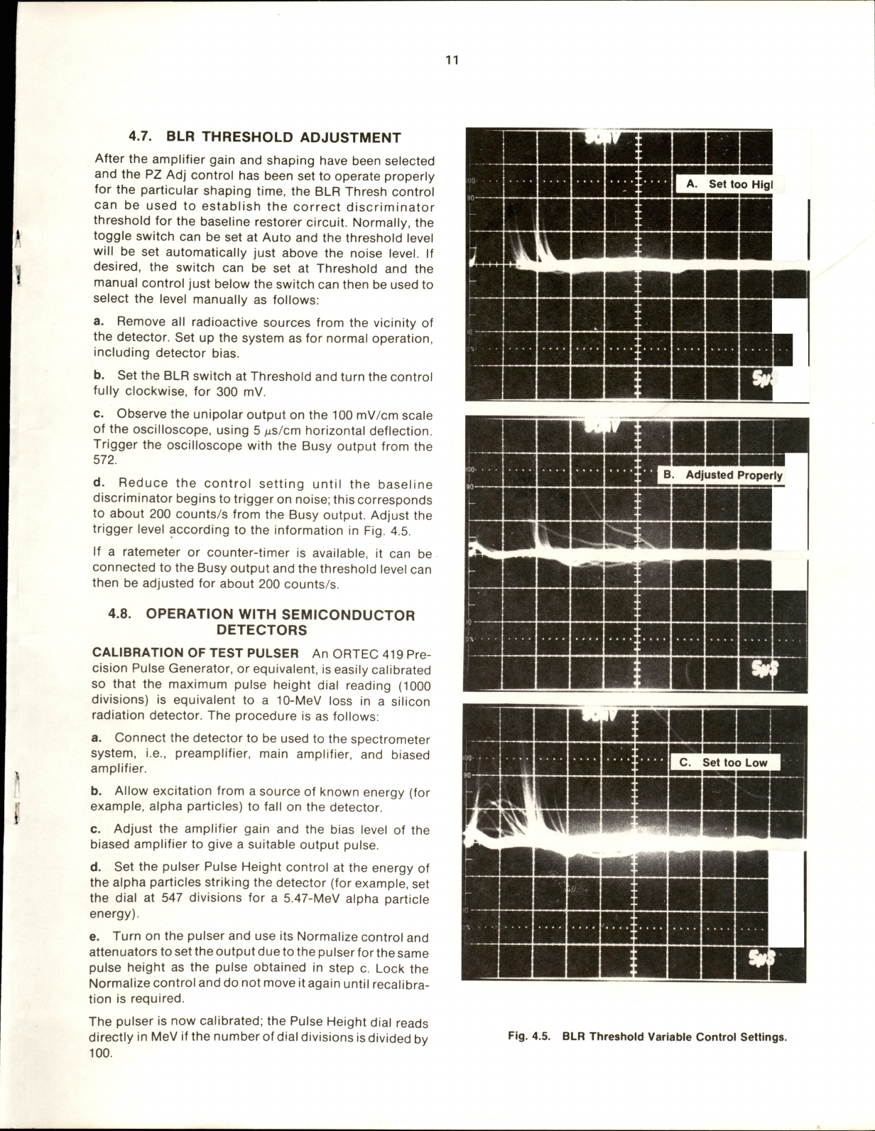
11
4.7.
BLR
THRESHOLD
ADJUSTMENT
After
the
amplifier
gain
and
shaping
have
been
seiected
and
the
PZ
Adj
control
has
been
set
to
operate
properly
for
the
particular
shaping
time,
the
BLR
Thresh
control
can
be
used
to
establish
the
correct
discriminator
threshold
for
the
baseline
restorer
circuit.
Normally,
the
toggle
switch
can
be
set
at
Auto
and
the
threshold
level
will
be
set
automatically
just
above
the
noise
level.
If
desired,
the
switch
can
be
set
at
Threshold
and
the
manual
control
just
below
the
switch
can
then
be
used
to
select
the
level
manually
as
follows:
a.
Remove
all
radioactive
sources
from
the
vicinity
of
the
detector.
Set
up
the
system
as
for
normal
operation,
including
detector
bias.
b.
Set
the
BLR
switch
at
Threshold
and
turn
the
control
fully
clockwise,
for
300
mV.
c.
Observe
the
unipolar
output
on
the
100
mV/cm
scale
of
the
oscilloscope,
using
5
/us/cm
horizontal
deflection.
Trigger
the
oscilloscope
with
the
Busy
output
from
the
572.
d.
Reduce
the
control
setting
until
the
baseline
discriminator
begins
to
trigger
on
noise;
this
corresponds
to
about
200
counts/s
from
the
Busy
output.
Adjust
the
trigger
ievel
according
to
the
information
in
Fig.
4.5.
If
a
ratemeter
or
counter-timer
is
available,
it
can
be
connected
to
the
Busy
output
and
the
threshold
level
can
then
be
adjusted
for
about
200
counts/s.
4.8.
OPERATION
WITH
SEMICONDUCTOR
DETECTORS
CALIBRATION
OF
TEST
PULSER
An
ORTEC
419
Pre
cision
Pulse
Generator,
or
equivalent,
is
easily
calibrated
so
that
the
maximum
pulse
height
dial
reading
(1000
divisions)
is
equivalent
to
a
10-MeV
loss
in
a
silicon
radiation
detector.
The
procedure
is
as
foilows:
a.
Connect
the
detector
to
be
used
to
the
spectrometer
system,
i.e.,
preamplifier,
main
amplifier,
and
biased
ampiifier.
b.
Allow
excitation
from
a
source
of
known
energy
(for
example,
alpha
particles)
to
fall
on
the
detector.
c.
Adjust
the
amplifier
gain
and
the
bias
level
of
the
biased
amplifier
to
give
a
suitable
output
pulse.
d.
Set
the
pulser
Pulse
Height
control
at
the
energy
of
the
alpha
particles
striking
the
detector
(for
example,
set
the
dial
at
547
divisions
for
a
5.47-MeV
alpha
particle
energy).
e.
Turn
on
the
pulser
and
use
its
Normalize
control
and
attenuators
to
set
the
output
due
to
the
pulser
for
the
same
pulse
height
as
the
pulse
obtained
in
step
c.
Lock
the
Normalize
control
and
do
not
move
it
again
untii
recalibra-
tion
is
required.
The
pulser
is
now
calibrated;
the
Pulse
Height
dial
reads
directly
in
MeV
if
the
number
of
dial
divisions
is
divided
by
100.
A.
Set
too
Higl
B.
Adjusted
Properly
C.
Set
too
Low
Fig.
4.5.
BLR
Tlireshold
Variable
Control
Settings.

12
AMPLIFIER
NOISE
AND
RESOLUTION
MEASURE
MENTS
As
shown
in
Fig.
4.6,
a
preamplifier,
amplifier,
pulse
generator,
oscilloscope,
and
wide-band
rms
volt
meter
such
as
the
Hewlett-Packard
3400A
are
required
for
this
measurement.
Connect
a
suitable
capacitor
to
the
input
to
simulate
the
detector
capacitance
desired.
To
obtain
the
resolution
spread
due
to
amplifier
noise:
a.
Measure
the
rms
noise
voltage
(Ems)
at
the
amplifier
output.
b.
Turn
on
the
419
Precision
Pulse
Generator
and
adjust
the
pulser
output
to
any
convenient
readable
voltage,
E„,
as
determined
by
the
oscilloscope.
The
full
width
at
half
maximum
(FWHM)
resolution
spread
due
to
amplifier
noise
is
then
2.35
Erms
Edtal
/V(FWHM)
=
,
E„
where
Ed,ai
is
the
pulser
dial
reading
in
MeV
and
2.35
is
the
factor
for
rms
to
FWHM.
For
average-responding
voltmeters
such
as
the
Hewlett-Packard
400D,
the
measured
noise
must
be
multiplied
by
1.13
to
calculate
the
rms
noise.
ORTEC ORTEC
LINEAR
AMPLIFIER
OSCILLO
SCOPE
PREAMP
.
DETECTOR
.
OR
CAPACITOR
PULSE
GENERATOR
VOLTMETER
Fig.
4.6.
System
for
Measuring
Amplifier
and
Detector
Noise
Resolution.
The
resolution
spread
will
depend
on
the
total
input
capacitance,
since
the
capacitance
degrades
the
signal-
to-noise
ratio
much
faster
than
the
noise.
DETECTOR
NOISE-RESOLUTION
MEASUREMENTS
The
measurement
just
described
can
be
made
with
a
biased
detector
instead
of
the
external
capacitor
that
would
be
used
to
simulate
detector
capacitance.
The
resolution
spread
will
be
larger
because
the
detector
contributes
both
noise
and
capacitance
to
the
input.
The
detector
noise-resolution
spread
can
be
isolated
from
the
amplifier
noise
spread
if
the
detector
capacity
is
known,
since
(Nd..)'
+
(A/amp)'
=
(W.o.al)'
,
where
Moiai
is
the
total
resolution
spread
and
A/amp
is
the
amplifier
resolution
spread
when
the
detector
is
replaced
by
its
equivalent
capacitance.
The
detector
noise
tends
to
increase
with
bias
voltage,
but
the
detector
capacitance
decreases,
thus
reducing
the
resolution
spread.
The
overall
resolution
spread
will
depend
upon
which
effect
is
dominant.
Figure
4.7
shows
curves
of
typical
noise-resolution
spread
versus
bias
voltage,
using
data
from
several
ORTEG
silicon
surface-
barrier
semiconductor
radiation
detectors.
o
0.4
ORTEG
BA-030-007-300
ORTEG
BA-025-050-100
ORTEG
BA-025-100-1C0
ORTEG
BA-030-200-100
ORTEG
BA-045-450-100
50
Bias
Voltage
Fig.
4.7.
Noise
as
a
Function
of
Bias
Voltage.
AMPLIFIER
NOISE-RESOLUTION
MEASUREMENTS
USING
MCA
Probably
the
most
convenient
method
of
making
resolution
measurements
is
with
a
pulse
height
analyzer
as
shown
by
the
setup
illustrated
in
Fig.
4.8.
The
amplifier
noise-resolution
spread
can
be
measured
directly
with
a
pulse
height
analyzer
and
the
mercury
pulser
as
follows:
a.
Select
the
energy
of
interest
with
an
ORTEG
419
Precision
Pulse
Generator.
Set
the
amplifier
and
biased
amplifier
gain
and
bias
level
controls
so
that
the
energy
is
in
a
convenient
channel
of
the
analyzer.
100
DETECTOR
OR
CAPACITOR
r——1
I
ORTEC
1
I
GATED
BIAS
I
>
AMPLIFIER
j
L.
,
J
PULSE
GENERATOR
ORTEC
ORTEC
MULTI
CHANNEL
PULSE
HEIGHT
ANALYZER
PREAMP
ORTEC
LINEAR
AMPLIFIER
ORTEC
BIASED
AMPLIFIER
ORTEC
PULSE
STRETCHER
ORTEC
Fig.
4.8.
System
for
Measuring
Resolution
with
a
Pulse
Height
Analyzer.
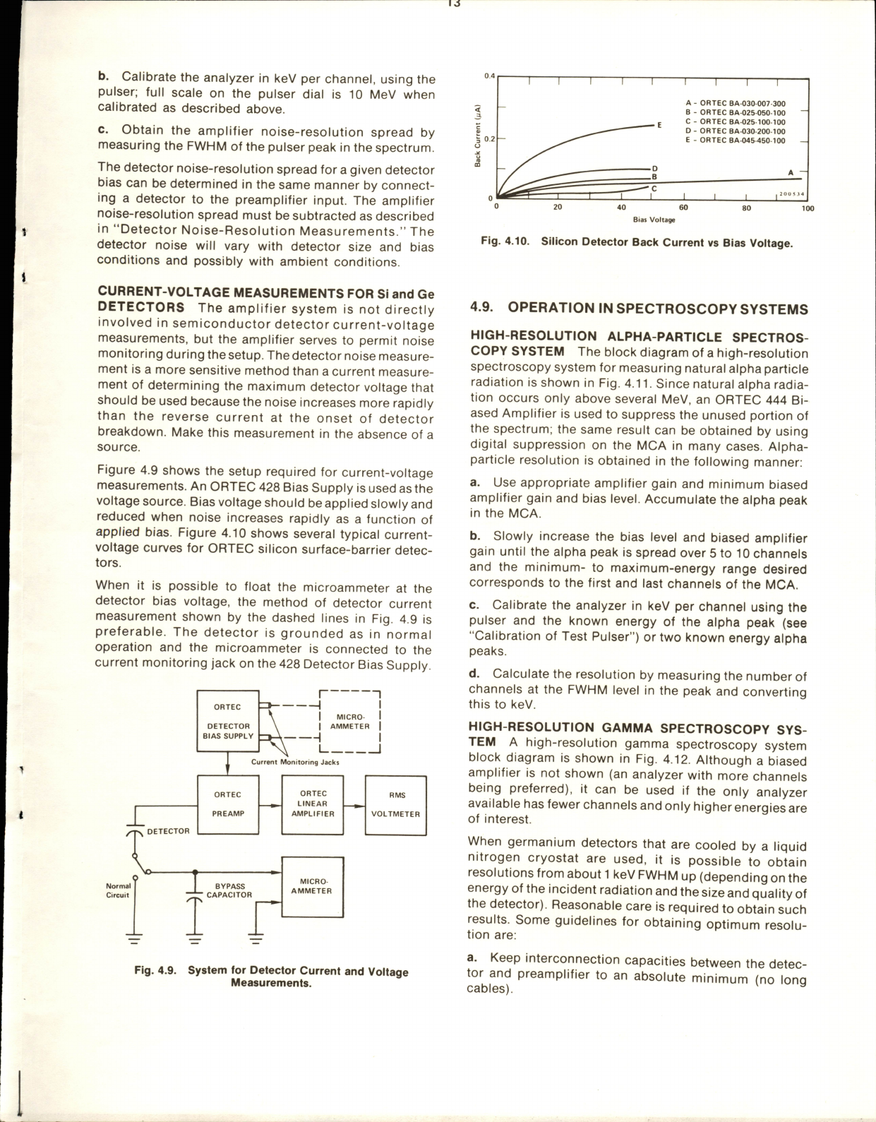
b.
Calibrate
the
analyzer
in
keV
per
channel,
using
the
pulser;
full
scale
on
the
pulser
dial
is
10
MeV
when
calibrated
as
described
above.
c.
Obtain
the
amplifier
noise-resolution
spread
by
measuring
the
FWHM
of
the
pulser
peak
in
the
spectrum.
The
detector
noise-resolution
spread
for
a
given
detector
bias
can
be
determined
in
the
same
manner
by
connect
ing
a
detector
to
the
preamplifier
input.
The
amplifier
noise-resolution
spread
must
be
subtracted
as
described
in
"Detector
Noise-Resolution
Measurements."
The
detector
noise
will
vary
with
detector
size
and
bias
conditions
and
possibly
with
ambient
conditions.
CURRENT-VOLTAGE
MEASUREMENTS
FOR
SI
and
Ge
DETECTORS
The
amplifier
system
is
not
directly
involved
in
semiconductor
detector
current-voltage
measurements,
but
the
amplifier
serves
to
permit
noise
monitoring
during
the
setup.
The
detector
noise
measure
ment
is
a
more
sensitive
method
than
a
current
measure
ment
of
determining
the
maximum
detector
voltage
that
should
be
used
because
the
noise
increases
more
rapidly
than
the
reverse
current
at
the
onset
of
detector
breakdown.
Make
this
measurement
in
the
absence
of
a
source.
Figure
4.9
shows
the
setup
required
for
current-voltage
measurements.
An
ORTEC
428
Bias
Supply
is
used
as
the
voltage
source.
Bias
voltage
should
be
applied
slowly
and
reduced
when
noise
increases
rapidly
as
a
function
of
applied
bias.
Figure
4.10
shows
several
typical
current-
voltage
curves
for
ORTEC
silicon
surface-barrier
detec
tors.
When
it
is
possible
to
float
the
microammeter
at
the
detector
bias
voltage,
the
method
of
detector
current
measurement
shown
by
the
dashed
lines
in
Fig.
4.9
is
preferable.
The
detector
is
grounded
as
in
normal
operation
and
the
microammeter
is
connected
to
the
current
monitoring
jack
on
the
428
Detector
Bias
Supply.
DETECTOR
BIAS
SUPPLY
1
I
j
\
1
AMMETER
j
I
Current
Monitoring
Jacks
ORTEC
PREAMP
ORTEC
LINEAR
AMPLIFIER
RMS
VOLTMETER
DETECTOR
Normal
Circuit
MICRO
AMMETER
BYPASS
-
CAPACITOR
Fig.
4.9.
System
for
Detector
Current
and
Voltage
Measurements.
0.4
0.2
4040
60
60
80
100
A
-
ORTEC
BA-030
007-300
B
-
ORTEC
BA-025
050-100
C
-
ORTEC
BA
025-100-100
D
-
ORTEC
BA-030.200-100
E
-
ORTEC
BA-045-450-100
Bias
Voltage
Fig.
4.10.
Silicon
Detector
Back
Current
vs
Bias
Voltage.
4.9.
OPERATION
IN
SPECTROSCOPY
SYSTEMS
HIGH-RESOLUTION
ALPHA-PARTICLE
SPECTROS
COPY
SYSTEM
The
block
diagram
of
a
high-resolution
spectroscopy
system
for
measuring
natural
alpha
particle
radiation
is
shown
in
Fig.
4.11.
Since
natural
alpha
radia
tion
occurs
only
above
several
MeV,
an
ORTEC
444
Bi
ased
Amplifier
is
used
to
suppress
the
unused
portion
of
the
spectrum;
the
same
result
can
be
obtained
by
using
digital
suppression
on
the
MCA
in
many
cases.
Alpha-
particle
resolution
is
obtained
in
the
following
manner:
a.
Use
appropriate
amplifier
gain
and
minimum
biased
amplifier
gain
and
bias
level.
Accumulate
the
alpha
peak
in
the
MCA.
b.
Slowly
increase
the
bias
level
and
biased
amplifier
gain
until
the
alpha
peak
is
spread
over
5
to
10
channels
and
the
minimum-
to
maximum-energy
range
desired
corresponds
to
the
first
and
last
channels
of
the
MCA.
c.
Calibrate
the
analyzer
in
keV
per
channel
using
the
pulser
and
the
known
energy
of
the
alpha
peak
(see
"Calibration
of
Test
Pulser")
or
two
known
energy
alpha
peaks.
d.
Calculate
the
resolution
by
measuring
the
number
of
channels
at
the
FWHM
level
in
the
peak
and
converting
this
to
keV.
HIGH-RESOLUTION
GAMMA
SPECTROSCOPY
SYS
TEM
A
high-resolution
gamma
spectroscopy
system
block
diagram
is
shown
in
Fig.
4.12.
Although
a
biased
amplifier
is
not
shown
(an
analyzer
with
more
channels
being
preferred),
it
can
be
used
if
the
only
analyzer
available
has
fewer
channels
and
only
higher
energies
are
of
interest.
When
germanium
detectors
that
are
cooled
by
a
liquid
nitrogen
cryostat
are
used,
it
is
possible
to
obtain
resolutions
from
about
1
keV
FWHM
up
(depending
on
the
energy
of
the
incident
radiation
and
the
size
and
quality
of
the
detector).
Reasonable
care
is
required
to
obtain
such
results.
Some
guidelines
for
obtaining
optimum
resolu
tion
are:
a.
Keep
interconnection
capacities
between
the
detec
tor
and
preamplifier
to
an
absolute
minimum
(no
long
cables).
^
Table of contents
Other EG&G Amplifier manuals

EG&G
EG&G ORTEC 113 Service manual

EG&G
EG&G ORTEC 427 User manual

EG&G
EG&G ORTEC 414A Service manual

EG&G
EG&G ORTEC 444 User manual

EG&G
EG&G ORTEC 118A User manual

EG&G
EG&G ORTEC 535 Service manual

EG&G
EG&G 113 Service manual

EG&G
EG&G ORTEC 855 Service manual

EG&G
EG&G ORTEC 485 User manual

EG&G
EG&G 128A Service manual


