EG&G ORTEC 485 User manual

100
MIDLAND
ROAD
OAK
RIDGE,
TENN.
37830
PHONE
(615)
482-1GGB
TWX
81G-572-1G7B
INSTRUCTION
MANUAL
485
AMPLIFIER
n
(z:oi\/ii=»ArsiY
INSTRUCTION
MANUAL
485
AMPLIFIER
Serial
No.
Purchaser
Date
issued.
I
Ci;
CD
F=1
(=>
CD
F=l
AT"
E
CD
100
MIDLAND
RDAD
DAK
RIDGE,
TENN.
37830
PHDNE
[615)
482-4411
TWX
81D-572
-1078
©
ORTEC
Incorporated
1968
Printed
In
U.S.A.

TABLE
OF
CONTENTS
Page
WARRANTY
PHOTOGRAPH
1.
DESCRIPTION
1 1
1.1
General
Description
1 1
1.2
Pole-Zero
Cancellation
1
1
1.3
Active
Filter
1
3
2.
SPECIFICATIONS
2
1
2.1
General
Specifications
2
1
2.2
Amplifier
Specifications
2
1
3.
INSTALLATION
3
1
3.1
General
Installation
Considerations
3
1
3.2
Connection
to
Preamplifier
3
1
3.3
Connection
of
Test
Pulse
Generator
3
1
3.4
Connection
to
Power
-
Nuclear
Standard
Bin,
ORTEC
401A/402A
3
2
3.5
Output
Connections
and
Terminating
Considerations
3
2
3.6
Shorting
the
Amplifier
Output
3
2
4.
OPERATING
INSTRUCTIONS
4
1
4.1
Controls
and
Connectors
4
1
4.2
Initial
Testing
and
Observation
of
Pulse
Waveforms
4
2
4.3
General
Considerations
for
Operation
with
Semiconductor
Detectors
4
2
4.4
Operation
in
Spectroscopy
Systems
4
7
4.5
Typical
System
Block
Diagrams
4
10
5.
CIRCUIT
DESCRIPTION
5
1
5.1
General
Block
Diagram
5
1
5.2
Circuit
Description
5
1
5.3
Circuit
Modifications
for
Special
Applications
5
3
6.
MAINTENANCE
6
1
6.1
Test
Equipment
Required
6
1
6.2
Pulser
Modifications
for
Overload
Tests
6
2
6.3
Pulser
Tests
and
Calibration
6
4
6.4
Tabulated
Test
Point
Voltages
SCHEMATIC
485-0101-S1
ORTEC
485
Amplifier
Schematic

LIST
OF
FIGURES
AND
ILLUSTRATIONS
Page
Figure
1.1
Differentiation
In
a
Non-Pole-Zero
Cancelled
Amplifier
Figure
1.2
Differentiation
(Clipping)
in
a
Pole-Zero
Cancelled
Amplifier
Figure
1.3
Pulse
Shapes
for
Good
Signal-to-Noise
Ratios
Figure
1.4
ORTEC
485
Active
Filter
Figure
4.1
Measuring
Amplifier
and
Detector
Noise
Resolution
Figure
4.2
Resolution
Spread
Versus
External
Input
Capacity
Figure
4.3
Amplifier
and
Detector
Noise
Versus
Bias
Voltage
Figure
4.4
Measuring
Resolution
with
a
Pulse
Height
Analyzer
Figure
4.5
Measuring
Detector
Current-Voltage
Characteristics
Figure
4.6
Silicon
Detector
Back
Current
Versus
Bias
Voltage
Figure
4.7
High
Resolution
Alpha
Particle
Spectroscopy
System
Figure
4.8
High
Resolution
Gamma
Spectroscopy
System
Using
a
Lithium
Drifted
Germanium
Detector
Figure
4.9
Scintillation
Counter
Gamma
Spectroscopy
System
Figure
4.10
High
Resolution
X-Ray
Spectroscopy
System
Figure
4.11
Gamma
Ray-Gamrtia
Coincidence
Experiment
-
Block
Diagram
Figure
4.12
Gamma
Ray-Charged
Particle
Coincidence
Experiment
-
Block
Diagram
Figure
4.13
Gamma
Ray
Pair
Spectrometer
-
Block
Diagram
Figure
5.1
485
Amplifier
Block
Diagram
Figure
5.2
ORTEC
485
Attenuator
Networks
Figure
6.1
Pulser
Modification
for
Overload
Tests
Figure
6.2
Pulser
Pole'zero
Cancellation
Figure
6.3
Method
for
Measuring
Nonlinearity
Figure
6.4
Method
for
Measuring
Crossover
Walk
1-2
1
-2
1
-4
1-5
4-3
4-3
4
4
4
4
4
4
4
4
4
4
4
5
5
6
6
6
6
4
5
6
6
7
8
9
10
11
11
12
1
2
1
2
3
3

A
NEW
STANDARD
TWO-YEAR
WARRANTY
FOR
ORTEC
ELECTRONIC
INSTRUMENTS
ORTEC
warrants
its
nuclear
instrument
products
to
be
free
from
defects
in
workmanship
and
materials,
other
than
vacuum
tubes
and
semiconductors,
for
a
period
of
twenty-four
months
from
date
of
shipment,
provided
that
the
equipment
has
been
used
in
a
proper
manner
and
not
subjected
to
abuse.
Repairs
or
replacement,
at
ORTEC
option,
will
be
made
without
charge
at
the
ORTEC
factory.
Shipping
expense
will
be
to
the
account
of
the
customer
except
in
cases
of
defects
discovered
upon
initial
operation.
Warranties
of
vacuum
tubes
and
semiconductors,
as
made
by
their
manufacturers,
will
be
extended
to
our
customers
only
to
the
extent
of
the
manufacturers'
liability
to
ORTEC.
Specially
selected
vacuum
tubes
or
semiconductors
cannot
be
warranted.
ORTEC
reserves
the
right
to
modify
the
design
of
its
products
without
incurring
responsibility
for
modification
of
previously
manufactured
units.
Since
installation
conditions
are
beyond
our
control,
ORTEC
does
not
assume
any
risks
or
liabilities
associated
with
methods
of
installation
other
than
specified
in
the
instructions,
or
installation
results.
QUALITY
CONTROL
Before
being
approved
for
shipment,
each
ORTEC
instrument
must
pass
a
stringent
set
of
quality
control
tests
designed
to
expose
any
flaws
in
materials
or
workmanship.
Permanent
records
of
these
tests
are
maintained
for
use
in
warranty
repair
and
as
a
source
of
statistical
information
for
design
improvements.
REPAIR
SERVICE
ORTEC
instruments
not
in
warranty
may
be
returned
to
the
factory
for
repairs
or
checkout
at
modest
expense
to
the
customer.
Standard
procedure
requires
that
returned
instruments
pass
the
same
quality
control
tests
as
those
used
for
new
production
instruments.
Please
contact
the
factory
for
instructions
before
shipping
equipment.
DAMAGE
IN
TRANSIT
Shipments
should
be
examined
immediately
upon
receipt
for
evidence
of
external
or
concealed
damage.
The
carrier
making
delivery
should
be
notified
immediately
of
any
such
damage,
since
the
carrier
is
normally
liable
for
damage
in
shipment.
Packing
materials,
waybills,
and
other
such
documentation
should
be
preserved
in
order
to
establish
claims.
After
such
notification
to
the
carrier,
please
notify
ORTEC
of
the
circumstances
so
that
we
may
assist
in
damage
claims
and
in
providing
replacement
equipment
if
necessary.

-i
V,-
.
■,Vj.;'
.
ORTEC®
^
MODEL
485
€
AMPLIFIER
COARSE
GAIN
16
FINE
GAIN
PZ-TRIM
POS
UNIPOLAR
t>
■#•
NEG
BIPOLAR
INPUT
OUTPUT
@
HH
i■
M-A
-I.
-
?5'-
-
■
*.?!■■
■
•

1
-1
ORTEC
485
AMPLIFIER
1.
DESCRIPTION
1.1
General
Description
The
ORTEC
485
Amplifier
is
a
functional
design
utilizing
integrated
circuits
to
provide
a
general
purpose
amplifier
at
minimum
cost.
The
low
input
noise,
dynamic
gain
range,
and
pulse
shaping
networks
allow
operation
with
semiconductor
detectors
and
scintillation
detectors
in
a
wide
variety
of
applications.
The
performance
capability
of
the
485
coupled
with
its
low
cost
will
allow
a
wide
range
of
uses
in
such
fields
as
research,
counting
rooms,
monitoring
applications,
and
instructional
laboratories.
The
instrument
has
a
single
linear
output
which
can
be
switch
selected
for
either
unipolar
or
bipolar
pulse
shape.
The
first
differentiation
network
has
variable
pole-zero
cancellation
which
can
be
adjusted
to
match
preamplifiers
with
greater
than
40/itsec
decay
times.
Excellent
overload
performance
is
accom
plished
by
the
use
of
pole-zero
techniques.
In
addition,
the
amplifier
contains
an
active
filter
shaping
network
which
optimizes
the
signal-to-noise
ratio
and
minimizes
the
overall
resolving
time.
The
485
can
be
used
for
crossover
timing
when
used
in
conjunction
with
an
ORTEC
407
Crossover
Pickoff
or
a
420
Timing
Single
Channel
Analyzer.
The
420
Timing
Single
Channel
Analyzer
output
has
a
minimum
of
walk
as
a
function
of
pulse
amplitude
and
incorporates
a
variable
delay
time
on
the
out
put
pulse
to
enable
the
crossover
pickoff
output
to
be
placed
in
time
coincidence with
other
outputs.
The
485
has
complete
provisions,
including
power,
for
operating
any
ORTEC
solid
state
preamplifier
such
as
the
109A,
113,
and
118A.
Preamplifier
pulses
should
have
a
rise
time
of
0.25;usec
or
less
to
properly
match
the
amplifier
filter
network,
and
a
decay
time
of
greater
than
40)usec
for
proper
pole-zero
cancellation.
The
input
impedance
is
1000
ohms.
When
long
preamplifier
cables
are
used,
the
cables
can
be
terminated
in
series
at
the
preamplifier
end
or
in
shunt
at
the
amplifier
end
with
the
proper
resistance.
The
output
impedance
of
the
485
is
about
0.5
ohm.
The
output
can
be
connected
to
other
equipment
by
either
a
single
cable
going
to
all
equipment
and
shunt
terminated
at
the
far
end
(and
series
ter
minated
at
the
amplifier
if
reflections
are
a
problem)
or
separate
cables
to
each
instrument
with
each
cable
series
terminated
at
the
amplifier.
(See
Section
3.5.)
Gain
changing
is
accomplished
by
constant
impedance
T
attenuators.
By
using
this
technique,
the
bandwidth
of
the
feedback
amplifier
stages
involved
in
gain
switching
remains
essentially
constant
regardless
of
gain
and
therefore
rise
time
changes
with
gain
switching
(which
cause
crossover
walk)
are
limited
to
small
capacitance
effects
across
the
attenuators.
The
485
is
one
NIM
standard
module
wide.
The
unit
has
no
self-contained
power
supply;
power
is
ob
tained
from
a
NIM
standard
Bin
and
Power
Supply
such
as
the
ORTEC
401A/402A.
The
485
design
is
consistent
with
other
modules
in
the
ORTEC
Modular
Nuclear
Instrumentation
Series;
i.e.,
it
is
not
possible
to
overload
the
bin
power
supply
with
a
full
complement
of
ORTEC
modules
in
the
bin.
Since
twelve
485
amplifiers
can
be
contained
and
powered
in
one
Bin
and
Power
Supply,
the
485
is
particularly
suited
to
experiments
requiring
many
amplifiers.
1.2
Pole-Zero
Cancellation
Pole-zero
cancellation
is
a
method
for
eliminating
pulse
undershoot
after
the
first
differentiating
network.
The
technique
employed
is
described
by
referring
to
the
waveforms
and
equations
shown
in
Figure
1.1
and
1.2.
In
a
non-pole-zero
cancelled
amplifier,
the
exponential
tail
on
the
preamplifier
output
signal
(usually
50
to
500/tsec)
causes
an
undershoot
whose
peak
amplitude
is
roughly:
Undershoot
Amplitude
_
Differentiation
Time
Differentiated
Pulse
Amplitude
Preamplifier
Pulse
Decay
Time

1
-2
(V
^max
®
200409
Undershoot
First
Charge
loop
clipping
P"
"
with
network
undershoot
Equations:
-t
Emax
^
1
s
F
X
=
f
I
(s);
Laplace
Transform
'^max
1 1
I
>
/.
r-
-t
^max
—
Ti
-
To
/^.
u
-r
d
To
e
-T^e
=
Ci
where
Ti
=
R
i
Cj
T
o-T,
Figure
1-1.
Differentiation
in
a
Non-Pole-Zero
Cancelled
Amplifier
><K
<1
So
(t)
e
T
K
ii
S—
—VNA*
>R3
Rj
i
r
-1-^
«!
(t)
No
Undershoot
Pole-zero
,
cancelled
_
Clipped
pulse
Charge
loop
x
-
vvithout
clipping
output
network
undershoot
1
K
Pole
zero
cancel
by
letting
s
+
——
s
+
■
T
o
R2C1
or:
^max^'^'^G(t)=e,
(t)
s
-I-
^
X
=
E\
(s);
Laplace
Transform
-max
1
"
Ri
-rR2
^^T^
'""RiRjC,
Emax
Efy^gx
Ri
-r
R2
1
s
+
„
„
„
s
+
R
R1
R2
£,
(s);
where
Rp
=
^^
]R2
Cj
RpCi
-t
200410
Figure
1-2.
Differentiation
(Clipping)
in
a
Pole-Zero
Cancelled
Amplifier

1-3
For
a
l^isec
differentiation
time
and
a
50jusec
preamplifier
pulse
decay
time,
the
maximum
undershoot
is
2%
and
decays
with
a
BOfisec
time
constant.
Under
overload
conditions,
this
undershoot
is
often
sufficiently
large
to
saturate
the
amplifier
during
a
considerable
portion
of
the
undershoot,
causing
excessive
deadtime.
This
effect
can
be
reduced
by
increasing
the
preamplifier
pulse
decay
time
(which
generally
reduces
the
counting
rate
capabilities
of
the
preamplifier)
or
compensating
for
the
undershoot
by
using
pole-zero
cancellation.
Pole-zero
cancellation
is
accomplished
by
the
network
shown
in
Figure
1.2.
The
pole
(
^
^
)
due
to
b
-(•
1
/Tq
the
preamplifier
pulse
decay
time
is
cancelled
by
the
zero
(S
+
K/R^Ci)
of
the
network.
In
effect,
the
dc
path
across
the
differentiation
capacitor
adds an
attenuated
replica
of
the
preamplifier
pulse
to
just
cancel
the
negative
undershoot
of
the
clipping
network.
Total
preamplifier
-
amplifier
pole-zero
cancellation
requires
that
the
preamplifier
output
pulse
decay
time
be
a
single
exponential
decay
and
matched
to
the
pole-zero
cancellation
network.
The
variable
pole-zero
cancellation
network
allows
accurate
cancellation
for
all
preamplifiers
having
40^isec
or
greater
decay
times.
The
network
is
factory
adjusted
to
BO^isec
which
is
compatible
with
all
ORTEC
FET
preamplifiers.
Improper
matching
of
the
pole-zero
cancellation
network
will
degrade
the
overload
performance
and
cause
excessive
pile-up
distortion
at
medium
counting
rates.
Improper
matching
causes
either
an
undercompensation
(undershoot
is
not
eliminated)
or
an
overcompensation
(output
after
the
main
pulse
does
not
return
to
the
baseline
and
decays
to
the
baseline
with
the
preamplifier
time
con
stant).
The
pole-zero
trim
is
accessible
from
the
front
panel
of
the
485
and
can
easily
be
adjusted
by
observing
the
baseline
with
a
monoenergetic
source
or
pulsar
having
the
same
decay
time
as
the
preamp
lifier
under
overload
conditions.
1.3
Active
Filter
When
only
grid
current
and
shot
noise
(gate
current
and
drain
thermal
noise
for
an
FET)
are
considered,
the
best
signal-to-noise
ratio
occurs
when
the
two
noise
contributions
are
equal
for
a
given
pulse
shape.
Also
at
this
point,
there
is
an
optimum
pulse
shape
for
the
optimum
signal-to-noise
ratio.
Unfor
tunately,
this
shape
(the
cusp
shown
in
Figure
1.3)
is
not
physically
realizable
and
very
difficult
to
simulate.
A
pulse
shape
that
can
be
simulated
(the
Gaussian
in
Figure
1.3)
requires
a
single
RC
differentiate
and
n
equal
RC
integrates,
where
n
approaches
infinity.
The
Laplace
transform
of
the
transfer
function
is:
^
^
GS
=,=
X
n
°o
t^Rc]
h
Rc]
where
the
first
term
is
the
single
differentiate
and
the
second
term
is
the
n
integrates.
The
485
active
filter
attempts
to
simulate
this
transfer
function
with
the
simplest
possible
circuit.
The
485
active
filter
circuit
is
shown
in
Figure
1.4.
The
major
attraction
of
the
active
RC
filter
is
the
simple
synthesis
of
a
complex
pulse
shape
resulting
in
a
significant
reduction
in
size,
complexity
and
cost.
For
a
given
resolving
time
(RC),
the
time
response
of
the
filter
network
depends
only
on
K
(see
the
circuit
equations
in
Figure
1.4).
For
K
=
1,
the
transfer
function
simplifies
to:
1
1
eo_
R^C^
_
R^C^
which
is
an
n
=
2
approximation
to
the
Gaussian
pulse
shape
(see
Figure
1.3).
For
K
=
2
(the
actual
case
for
the
ORTEC
filter),
the
transfer
function
becomes:
Bq,
R'^C^
R^C^
ei
■J
c2
r-.
-
2s
2
i;
i+jir-
i-i1
i=V^
S
+ +
^ ^
'
I
Icj.
'
I
'
V
RC
R^C^

1
-4
CUSP
-t/RC
t/RC
t
>0
t
<
0
GAUSSIAN
(S+l/RC)
(S+l/llC)
n
GAUSSIAN
APPROXIMATION
FOR
n=2
1
(S+l/RC)
(S+1/RC)^
200362
ACTIVE
FILTER
V
rcA
rc/
j=xFT
Figure
1-3.
Pulse
Shapes
for
Good
Signal-to-Nolse
Ratios

1-5
In
this
case,
the
complex
roots
cause
an
underdamped
effect
which
reduces
the
resolving
time
and
results
in
a
more
symmetrical
pulse
shape
(see
Figure
1.3).
The
485
is
manufactured
with
1/isec
time
constants
(R
=
1000f2,
C
=
lOOOpF,
C/K
=
500pF).
These
time
constants
can
be
changed
to
suit
the
experiment.
See
Section
5.3
for
details
on
this
modification.
R
R
e:
e„
-Wv-
C
-L
*
£
^
K
Equations:
K
SC
K
®o
-
ea
—
ea
K
"K
+
SRC
ei
-
ea ea
-
eo
ea
-
Bq
SC
Eliminating
ea
and
solving
for
the
transfer
function:
R^
eo
®i
.
2S
.
K
+
^
+
RC
R2C2
Figure
1.4.
ORTEC
485
Active
Filter
2-1
2.
SPECIFICATIONS
2.1
General
Specifications
2.1.1
The
485
is
intended
for
use
with
a
Nuclear
Standard
Bin
such
as
the
ORTEC
401A/402A.
Two
watts
of
power
is
required
for
the
operation
of
the
485
in
the
quiescent
condition.
The
401A/-
402A
can
be
operated
on
either
115
or
220
volts
ac,
50-60
Hz;
if
it
is
used
with
220
volts
ac,
the
manual
for
the
401A/402A
must
be
referred
to
in
order
to
ensure
that
correct
connections
have
been
made
before
operation
on
220
volts
ac
is
attempted.
The
instrument
is
supplied
from
the
factory
wired
for
115
volts
ac
operation.
The
power
input
connector
to
the
401A/402A
is
a
NEMA
standard
3-wire
grounding
type.
Preamplifier
power
of
±12V
and
±24V
is
available
on
the
485
rear
panel
connector,
CN3.
All
signal
inputs
and
outputs
are
on
BNC
connectors
which
are
mounted
on
the
front
panel.
2.1.2
The
instrument
is
intended
for
rack
mounting
in
a
401A/402A
Nuclear
Standard
Bin,
but
the
Nuclear
Standard
Bin
is
suitably
packaged
for
cabinet
installation
if
desired.
The
weight
of
the
485
is
2
pounds
and
its
outside
dimensions
are
approximately
8.75
inches
high
by
1.35
inches
wide
by
9.75
inches
deep.
2.2
Amplifier
Specifications
INPUT:
Input
pulse
should
have
less
than
0.25Msec
rise
time
for
best
filter
action,
40;usec
minimum
decay
time
for
pole-zero
cancellation,
^2\l
maximum,
6V
maximum
to
prevent
saturation
before
differentiation,
1000
ohms
impedance,
dc-coupled
OUTPUT:
Positive
or
bipolar,
0-1OV
linear
with
11.5V
saturation
into
1000
ohms.
0-9V
linear
with
10V
saturation
into
100
ohms,
0.5
ohm
output
impedance
SHAPING:
Active
network
filter
resulting
in
approximately
Gaussian
shape,
peak
amplitude
at
1.5/isec
for
unipolar
and
l.ljusec
for
double
clip,
crossover
at
2.5;usec
for
bipolar
MAXIMUM
GAIN:
640
GAIN
CHANGE
RANGE:
107:1
total,
32:1
in
factors
of
2
by
switches
with
1%
accuracy,
3:1
continuous
fine
control
LINEARITY:
±0.15%
over
specified
linear
range
NOISE:
10/uV
at
maximum
gain
and
single
clip,
12/xV
at
maximum
gain
and
double
clip,
both
referred
to
input
SHORT
CIRCUIT
LIMITS:
The
amplifier
will
sustain
a
direct
short
on
the
output
for
an
indefinite
period
for
counting
rates
up
to
10^
Hz
COUNTING
RATE:
Less
than
0.5%
gain
shift
and
0.25%
resolution
spread
fullwidth
at
half
maximum
for
a
pulser
peak
above
a
50K
cts/sec
'
^
'Cs
background
OVERLOAD:
Recovery
within
2%
of
rated
output
from
600
times
overload
in
2.5
non-overloaded
pulse
widths
(25iisec)
at
maximum
gain
and
specified
input
CROSSOVER
WALK:
±3
nsec
for
10:1
dynamic
range
with
1;usec
bipolar
shaping
(including
amplifier
and
ORTEC
420
Timing
Single
Channel
Analyzer)
OPERATING
TEMPERATURE:
0
to
50^0
TEMPERATURE
STABILITY:
0.02%/oc
POWER
REQUIRED:
(Supplied
by
401A/402A
Power
Supply)
+24
V,
35
mA;
-24
V,
20
mA;
+12
V,50
mA;-12
V,
70
mA.

3-1
3.
INSTALLATION
3.1
General
Installation
Considerations
The
485,
used
in
conjunction
with
a
401A/402A
Bin
and
Power
Supply,is
intended
for
rack
mounting;
therefore,
it
is
necessary
to
ensure
that
vacuum
tube
equipment
operating
in
the
same
rack
with
the
485
has
sufficient
cooling
air
circulating
to
prevent
any
localized
heating
of
the
all-semiconductor
circuitry
used
throughout
the
485.
The
temperature
of
equipment
mounted
in
racks
can
easily
exceed
120OF
(50OC)
unless
precautions
are
taken.
3.2
Connection
to
Preamplifier
The
preamplifier
output
signal
is
connected
to
the
485
BNC
connector
CN1,
labeled
INPUT.
The
input
impedance
seen
at
the
input
is
1000
ohms
and
is
dc-coupled
to
ground;
therefore,
the
output
of
the
preamplifier
must
be
either
ac-coupled
or
have
no
dc
voltage
under
no
signal
conditions.
The
485
incorporates
pole-zero
cancellation
in
order
to
enhance
the
overload
characteristics
of
the
amplifier.
Thistechnique
requires
matching
the
network
to
the
preamplifier
decay
time
constant
in
order
to
achieve
perfect
compensation.
The
network
is
variable
and
factory
adjusted
to
50^tsec
to
match
all
ORTEC
FET
preamplifiers.
If
another
preamplifier
is
used
or
more
careful
matching
is
desired,
the
trim
is
accessible
from
the
front
panel.
Adjustment
is
easily
accomplished
by
using
a
monenergetic
source
and
observing
the
amplifier
baseline
after
each
pulse
overload
condition.
Preamplifier
power
of-h24V,
-t-12V,
-12V,
and
-24V
is
available
on
the
preamp
power
connector,
CN3.
When
using
the
485
with
a
remotely
located
preamplifier
(i.e.,
preamplifier-to-amplifier
connection
through
25
feet
or
more
of
coaxial
cable),
ensure
that
the
characteristic
impedance
of
the
transmission
line
from
the
preamplifier
output
to
the
485
input
is
matched.
Since
the
input
impedance
of
the
485
is
1000
ohms,
sending
end
termination
will
normally
be
preferred;
i.e.,
the
transmission
line
should
be
series
terminated
at
the
output
of
the
preamplifier.
All
ORTEC
preamplifiers
contain
series
terminations
which
are
either
93
ohms
or
variable.
3.3
Connection
of
Test
Pulse
Generator
3.3.1
Connection
of
Pulse
Generator
to
the
485
Through
a
Preamplifier
The
satisfactory
connection
of
atest
pulse
generator
such
as
the
ORTEC
419
or
equivalent
depends
primarily
on
two
considerations:
(1)
the
preamplifier
must
be
properly
connected
to
the
485
as
discussed
in
Section
3.2,
and
(2)
the
proper
input
signal
simulation
must
be
applied
to
the
preamplifier.
To
ensure
proper
input
signal
simulation,
refer
to
the
instruction
manual
for
the
particular
preamplifier
being
used.
3.3.2
Direct
Connection
to
Pulse
Generator
to
the
485
Since
the
input
of
the
485
has
1000
ohms
input
impedance,
the
test
pulse
generator
will
normally
have
to
be
terminated
at
the
amplifier
input
with
an
additional
shunt
resistor.
In
addition,
if
the
test
pulse
generator
has
a
dc
offset,
a
large
series
isolating
capacitor
is
also
required,
since
the
input
of
the
485
is
dc-coupled
to
the
first
amplifier
stage.
The
ORTEC
204
or
419
Test
Pulse
Generators
are
designed
for
direct
connection.
When
either
of
these
units
is
used,
it
should
be
terminated
with
a
100
ohm
terminator
at
the
amplifier
input.
(The
small
error
due
to
the
finite
input
imped
ance
of
the
amplifier
can
normally
be
neglected.)
3.3.3
Special
Test
Pulse
Generator
Considerations
for
Pole-Zero
Cancellation
The
pole-zero
cancellation
network
in
the
485
is
factory
adjusted
for
a
50^isec
decay
time
to
match
ORTEC
FET
preamplifiers.
When
a
tail
pulser
(such
as
the
204
or
419)
is
connected
directly
to
one
of
the
amplifier
inputs,
the
pulser
should
be
modified
to
obtain
a
50^isec
decay
time
if
overload
tests
are
to
be
made
(other
tests
are
not
affected).
See
Section
6.2
for
details
on
this
modification.

3-2
If
a
preamplifier
is
used
and
a
tail
pulser
connected
to
the
preamplifier
pulser
input,
similar
precautions
are
necessary.
In
this
case,
the
effect
of
the
pulser
decay
must
be
removed;
i.e.,
a
step
input
should
be
simulated.
Details
for
this
modification
are
given
in
Section
6.2.
3.4
Connection
to
Power
-
Nuclear
Standard
Bin,
ORTEC
401A/402A
The
485
contains
no
internal
power
supply;
therefore,
it
must
obtain
power
from
a
Nuclear
Standard
Bin
and
Power
Supply
such
as
the
401A/402A.
Turn
power
off
when
inserting
or
removing
modules.
The
ORTEC
Modular
Nuclear
Instrument
Series
is
designed
so
that
it
is
not
possible
to
overload
the
bin
power
supply
with
a
full
complement
of
modules
in
the
Bin.
This
may
not
be
true
when
the
Bin
contains
modules
other
than
those
of
ORTEC
design,
and
in
this
case,
check
the
power
supply
voltages
after
insertion
of
the
modules.
The
401A/402A
has
test
points
on
the
power
supply
control
panel
to
monitor
the
dc
voltages.
3.5
Output
Connections
and
Terminating
Considerations
The
485
linear
output
can
be
switch
selected
for
either
a
unipolar
or
a
bipolar
output.
The
unipolar
output
should
be
used
for
high
resolution
spectrometry
applications
with
semiconductor
detectors.
The
bipolar
output
should
be
used
in
applications
requiring
high
counting
rates
or
crossover
timing.
Typical
system
block
diagrams
for
a
variety
of
experiments
are
described
in
Section
4.
The
source
impedance
of
the
0-10
volt
standard
linear
outputs
of
most
ORTEC
modules
is
approxi
mately
1
ohm.
Interconnection
of
linear
signals
is
thus
non-critical,
since
the
input
impedance
of
circuits
to
be
driven
is
not
important
in
determining
the
actual
signal
span,
e.g.,
0-10
volts,
delivered
to
the
following
circuit.
Paralleling
several
loads
on
a
single
output
is
therefore
permissible
while
preserving
the
0-10
volt
signal
span.
Short
lengths
of
interconnecting
coaxial
cable
(up
to
approximately
4
feet)
need
not
be
terminated.
However,
if
a
cable
longer
than
approximately
4
feet
is
necessary
on
a
linear
output,
it
should
be
terminated
in
a
resistive
load
equal
to
the
cable
impedance.
Since
the
output
impedance
is
not
purely
resistive
and
is
slightly
different
for
each
individual
module
when
a
certain
given
length
of
coaxial
cable
is
connected
and
is
not
terminated
in
the
characteristic
impedance
of
the
cable,oscillations
will
occasionally
be
observed.
These
oscillations
can
be
suppressed
for
any
length
of
cable
by
properly
terminating
the
cable,
either
in
series
at
the
sending
end
or
in
shunt
at
the
receiving
end
of
the
line.
To
properly
terminate
the
cable
at
the
receiving
end,
it
may
be
necessary
to
consider
the
input
impedance
of
the
driven
circuit,
choosing
an
additional
parallel
resistor
to
make
the
combina
tion
produce
the
desired
termination
impedance.
Series
terminating
the
cable
at
the
sending
end
may
be
preferable
in
some
cases,
where
receiving
end
terminating
is
not
desirable
or
possible.
When
series
terminating
at
the
sending
end,
full
signal
span,
i.e.,
amplitude,
is
obtained
at
the
receiving
end
only
when
it
is
essentially
unloaded
or
loaded
with
an
impedance
many
times
that
of
the
cable.
This
may
be
accomplished
by
inserting
a
series
resistor
equal
to
the
characteristic
impedance
of
the
cable
internally
in
the
module
between
the
actual
amplifier
output
on
the
etched
board
and
the
output
connector.
This
impedance
is
in
series
with
the
input
impedance
of
the
load
being
driven,
and
in
the
case
where
the
driven
load
is
900
ohms,
a
decrease
in
the
signal
span
of
approximately
10%
will
occur
for
a
93-ohm
transmission
line.
A
more
serious
loss
occurs
when
the
driven
load
is
93
ohms
and
the
transmission
system
is
93
ohms.
In
this
case,
a
50%
loss
will
occur.
BNC
connectors
with
internal
terminators
are
available
from
a
number
of
connector
manufacturers
in
nominal
values
of
50,
100,
and
1000
ohms.
ORTEC
stocks
in
limited
quantity
both
the
50
and
100
ohm
BNC
terminators.
The
BNC
terminators
are
quite
convenient
to
use
in
conjunction
with
a
BNC
tee.
3.6
Shorting
the
Amplifier
Output
The
output
of
the
485
is
ac-coupled
with
an
output
impedance
of
about
0.5
ohm.
If
the
output
is
shorted
with
a
direct
short-circuit
and
the
amplifier
counting
rate
exceeds
10,000
counts
per
second,
the
output
stage
will
eventually
heat
up
sufficiently
to
destroy
itself
(about
one
minute
for
10
cts/sec).
The
amplifieroutput
may
be
shorted
indefinitely
without
catastrophic
damage
at
rates
below
lO"
cts/sec.

4-1
4.
OPERATING
INSTRUCTIONS
4.1
Controls
and
Connectors
4.1.1
Description
FINE
GAIN:
A
single-turn
fine
gain
control
is
provided
for
a
dynamic
range
of
3:1.
The
Fine
Gain
factor
is
selectable
from
X3
through
X10.
COARSE
GAIN:
Coarse
gain
control
is
provided
by
a
rotary
switch.
The
binary
selector
switch
covers
the
range
of
X2
to
X64.
UNIPOLAR-BIPOLAR:
Either
unipolar
or
bipolar
output
pulses
are
switch
selectable.
The
gains
are
matched
in
both
modes
to
approximately
±2.5%.
PZ-TRIM:
A
trim
potentiometer
is
provided
to
adjust
the
pole-zero
cancellation
network
for
varying
preamplifier
decay
times.
INPUT:
A
front
panel
BNC
connector
for
preamplifier
pulses
having
either
polarity.
Preamplifier
pulses
should
have
less
than
0.25;usec
rise
time
and
a
50/isec
decay
time.
POS-NEG:
A
switch
to
accommodate
either
positive
or
negative
input
signals
from
a
preamplifier.
OUTPUT:
A
front
panel
BNC
connector
providing
a
low
impedance
shaped
output,
with
a
test
probe
adjacent
for
oscilloscope
monitoring.
PREAMP:
A
connector
providing
±12
and
±24
volts
for
preamplifier
power.
This
furnishes
direct
compatibility
for
all
ORTEC
transistor
and
FET
preamps.
4.1.2
Front
and
Rear
Panel
Connector
Data
Connector
See
Dwg
485-0101-S1
Generic
Designation
Test
Point
Output
or
Input
Impedance
Shape
and
Amplitude
Limitations
CN-1
INPUT
No
1000J2
Positive
or
negative.
Less
than
0.25^tsec
rise
time
and
SOjusec
decay
time
is
rec
ommended,
although
faster
rise
and
slower
decay
times
can
be
handled.
6V
maxi
mum
linear,
12V
absolute
maximum
CN-2
CN-3
OUTPUT
PREAMP
POWER
TP-1
No
0.5J2
dc
Positive
or
bipolar,
0-10V
linear
with
11.5V
satura
tion
into
lOOOrZ,
0-9V
linear
with
10V
saturation
into
100J2,
approximate
Gaussian
shape
Pin
1:
Gnd
Pin
6:
-24V
Pin
7:
+24V
Pin
9:
-12V
Pin
4:
+12V
4-2
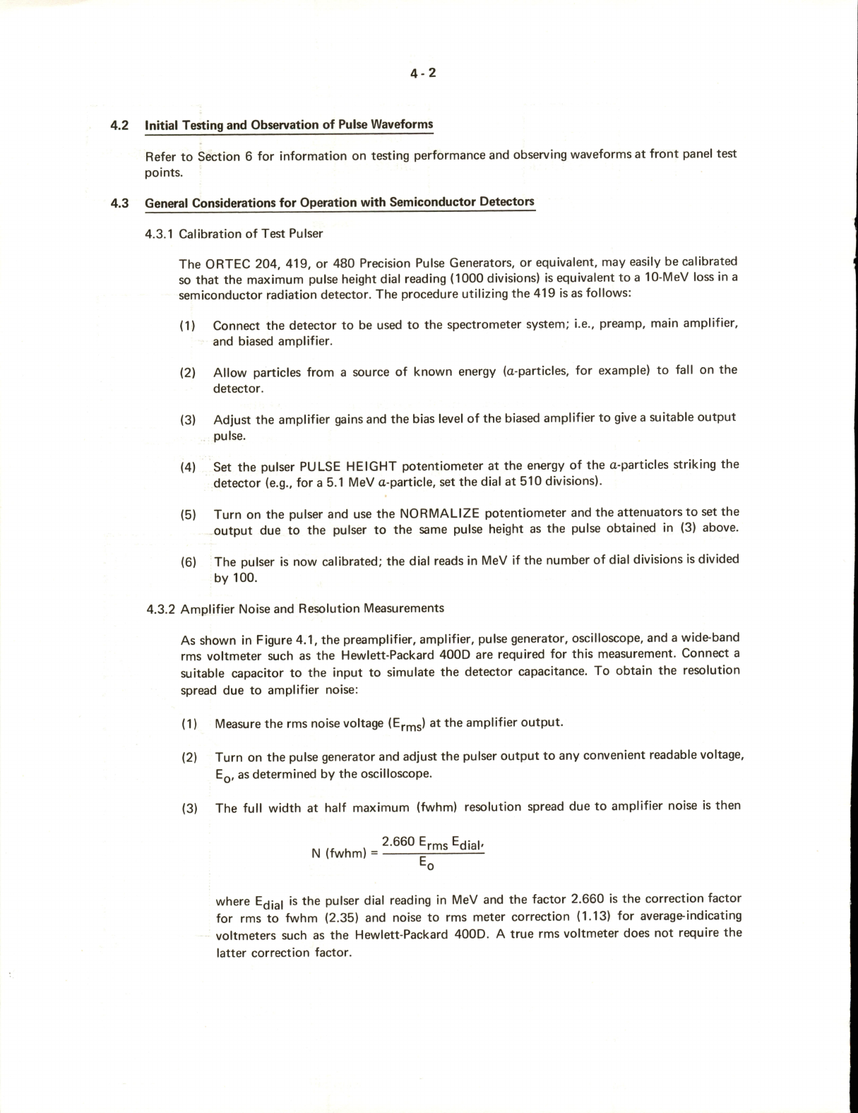
4.2
Initial
Testing
and
Observation
of
Pulse
Waveforms
Refer
to
Section
6
for
information
on
testing
performance
and
observing
waveforms
at
front
panel
test
points.
4.3
General
Considerations
for
Operation
with
Semiconductor
Detectors
4.3.1
Calibration
of
Test
Pulser
The
ORTEC
204,
419,
or
480
Precision
Pulse
Generators,
or
equivalent,
may
easily
be
calibrated
so
that
the
maximum
pulse
height
dial
reading
(1000
divisions)
is
equivalent
to
a
10-MeV
loss
in
a
semiconductor
radiation
detector.
The
procedure
utilizing
the
419
is
as
follows:
(1)
Connect
the
detector
to
be
used
to
the
spectrometer
system;
i.e.,
preamp,
main
amplifier,
and
biased
amplifier.
(2)
Allow
particles
from
a
source
of
known
energy
(a-particles,
for
example)
to
fall
on
the
detector.
(3)
Adjust
the
amplifier
gains
and
the
bias
level
of
the
biased
amplifier
to
give
a
suitable
output
pulse.
(4)
Set
the
pulser
PULSE
HEIGHT
potentiometer
at
the
energy
of
the
a-particles
striking
the
detector
(e.g.,
for
a
5.1
MeV
a-particle,
set
the
dial
at
510
divisions).
(5)
Turn
on
the
pulser
and
use
the
NORMALIZE
potentiometer
and
the
attenuators
to
set
the
output
due
to
the
pulser
to
the
same
pulse
height
as
the
pulse
obtained
in
(3)
above.
(6)
The
pulser
is
now
calibrated;
the
dial
reads
in
MeV
if
the
number
of
dial
divisions
is
divided
by
ICQ.
4.3.2
Amplifier
Noise
and
Resolution
Measurements
As
shown
in
Figure
4.1,
the
preamplifier,
amplifier,
pulse
generator,
oscilloscope,
and
a
wide-band
rms
voltmeter
such
as
the
Hewlett-Packard
400D
are
required
for
this
measurement.
Connect
a
suitable
capacitor
to
the
input
to
simulate
the
detector
capacitance.
To
obtain
the
resolution
spread
due
to
amplifier
noise:
(1)
Measure
the
rms
noise
voltage
(Ej-^pg)
at
the
amplifier
output.
(2)
Turn
on
the
pulse
generator
and
adjust
the
pulser
output
to
any
convenient
readable
voltage,
Eq,
as
determined
by
the
oscilloscope.
(3)
The
full
width
at
half
maximum
(fwhm)
resolution
spread
due
to
amplifier
noise
is
then
2.660
Epppg
E(jja|,
N
(fwhm)
Eo
where
Ejjjai
is
the
pulser
dial
reading
in
MeV
and
the
factor
2.660
is
the
correction
factor
for
rms
to
fwhm
(2.35)
and
noise
to
rms
meter
correction
(1.13)
for
average-indicating
voltmeters
such
as
the
Hewlett-Packard
400D.
A
true
rms
voltmeter
does
not
require
the
latter
correction
factor.
4-3
(DETECTOR
OR
CAPACITOR)
200162
LINEAR
AMP
ORTEC
VOLTMETER
RMS
PREAMPLIFIER
ORTEC
PULSE
GENERATOR
ORTEC
OSCILLOSCOPE
Figure
4.1.
Measuring
Amplifier
and
Detector
Noise
Resolution
The
resolution
spread
will
depend
upon
the
total
input
capacitance,
since
the
capacitance
degrades
the
signal-to-noise
ratio
much
faster
than
the
noise.
A
typical
resolution
spread
versus
external
input
capacitance
for
the
118A-435A
system
is
shown
in
Figure
4.2.
The
same
general
curve
is
applicable
with
the
109A-485
system,
although
the
intercept
on
the
keV
axis
will
be
higher.
100
0)
O
JC.
S
X
10
485
AMPLIFIER
118A
PREAMPLIFIER
^
M
sec
.
b
'ir
j
MMC
y
f
y
X
a
1
oiiTac
200073
10
100
EXTERNAL
INPUT
CAPACITY
(pf)
1000
Figure
4.2.
Resolution
Spread
Versus
External
Input
Capacity

4
-
4
4.3.3
Detector
Noise
Resolution
Measurements
The
same
measurement
described
in
Section
4.3.2
can
be
made
with
a
biased
detector
instead
of
the
external
capacitor
used
to
simulate
the
detector
capacitance.
The
resolution
spread
will
be
larger
because
the
detector
contributes
both
noise
and
capacitance
to
the
input.
The
detector
noise
resolution
spread
can
be
isolated
from
the
amplifier
noise
spread
if
the
detector
capacity
is
known,
since
Ndet^
+
Namp^
~
'^total^
where
N^Q^^gl
resolution
spread
and
Ngmp's
f^e
amplifier
resolution
spread
with
the
detector
replaced
by
its
equivalent
capacitance.
The
detector
noise
tends
to
increase
with
bias
voltage,
but
the
detector
capacitance
decreases,
thus
reducing
the
resolution
spread.
The
overall
resolution
spread
will
depend
upon
which
effect
is
dominant.
Figure
4.3
shows
curves
of
typical
total
noise
resolution
spread
versus
bias
voltage,
using
the
data
from
several
ORTEC
silicon
semiconductor
radiation
detectors.
.8
</)
I-
_j
o
>
(Si
o
z
(fi
s.
cr
0
A
-
ORTEC
BA-030-007-300
B
-
ORTEC
BA-025-050-100
.
C-
ORTEC
BA-025-100-100
U-
UK1tU
W
E
-
ORTEC
B/I
1-045^50-100
E
■>—
D
.c
—
F
.A
0
MTce
200159
25
100
125
50 75
BIAS
VOLTAGE
Figure
4.3.
Amplifier
and
Detector
Noise
Versus
Bias
Voltage
4.3.4
Amplifier
Noise
and
Resolution
Measurements
Using
a
Pulse
Height
Analyzer
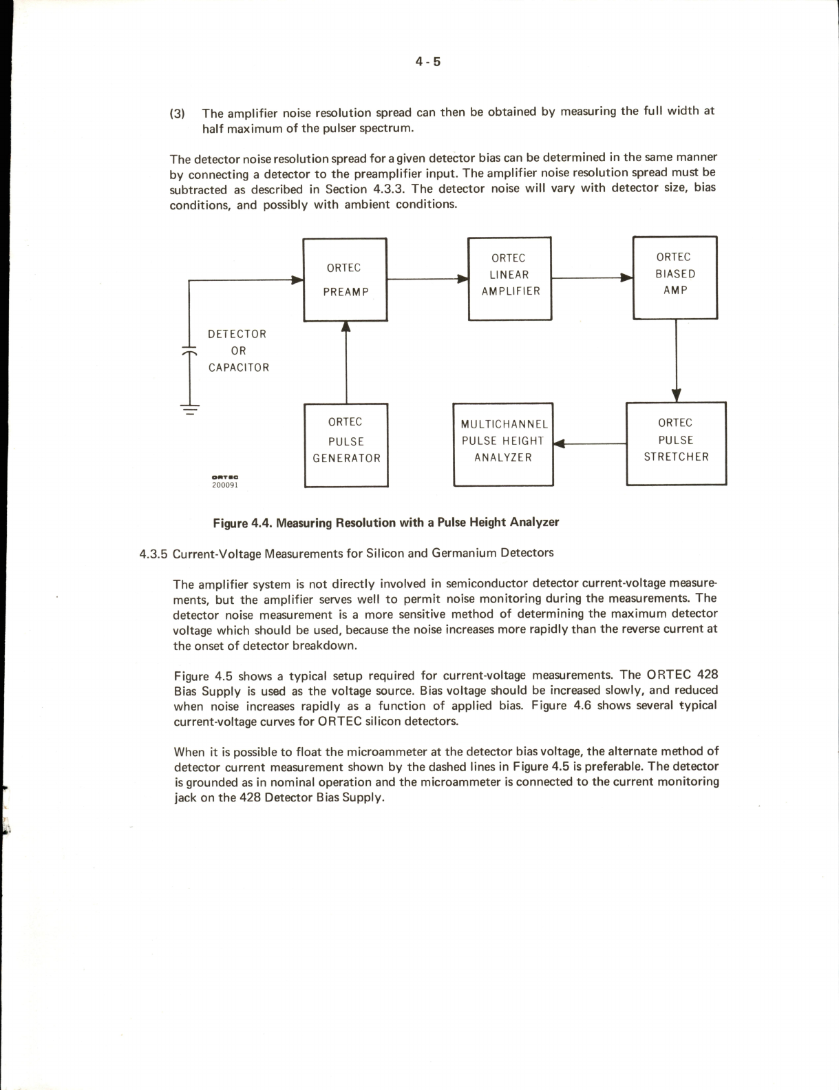
Probably
the
most
convenient
method
of
making
resolution
measurements
is
with
a
pulse
height
analyzer
as
shown
by
the
set-up
illustrated
in
Figure
4.4.
The
amplifier
noise
resolution
spread
can
be
measured
directly
with
a
pulse
height
analyzer
and
the
mercury
pulser
as
follows:
(1)
Select
the
energy
of
interest
with
an
ORTEC
419
Pulse
Generator,
and
set
the
Active
Filter
Amplifier
and
Biased
Amplifier
GAIN
and
BIAS
LEVEL
controls
so
that
the
energy
is
in
a
convenient
channel
of
the
analyzer.
(2)
Calibrate
the
analyzer
in
keV
per
channel,
using
the
pulser
(full
scale
on
the
pulser
dial
is
10
MeV
when
calibrated
as
described
in
Section
4.3.1.).
4-5
(3)
The
amplifier
noise
resolution
spread
can
then
be
obtained
by
measuring
the
full
width
at
half
maximum
of
the
pulser
spectrum.
The
detector
noise
resolution
spread
for
a
given
detector
bias
can
be
determined
in
the
same
manner
by
connecting
a
detector
to
the
preamplifier
input.
The
amplifier
noise
resolution
spread
must
be
subtracted
as
described
in
Section
4.3.3.
The
detector
noise
will
vary
with
detector
size,
bias
conditions,
and
possibly
with
ambient
conditions.
DETECTOR
OR
CAPACITOR
200091
ORTEC
LINEAR
AMPLIFIER
PULSE
GENERATOR
ORTEC
ORTEC
BIASED
AMP
PREAMP
ORTEC
ORTEC
PULSE
STRETCHER
MULTICHANNEL
PULSE
HEIGHT
ANALYZER
Figure
4.4.
Measuring
Resolution
with
a
Pulse
Height
Analyzer
4.3.5
Current-Voltage
Measurements
for
Silicon
and
Germanium
Detectors
The
amplifier
system
is
not
directly
involved
in
semiconductor
detector
current-voltage
measure
ments,
but
the
amplifier
serves
well
to
permit
noise
monitoring
during
the
measurements.
The
detector
noise
measurement
is
a
more
sensitive
method
of
determining
the
maximum
detector
voltage
which
should
be
used,
because
the
noise
increases
more
rapidly
than
the
reverse
current
at
the
onset
of
detector
breakdown.
Figure
4.5
shows
a
typical
setup
required
for
current-voltage
measurements.
The
ORTEC
428
Bias
Supply
is
used
as
the
voltage
source.
Bias
voltage
should
be
increased
slowly,
and
reduced
when
noise
increases
rapidly
as
a
function
of
applied
bias.
Figure
4.6
shows
several
typical
current-voltage
curves
for
ORTEC
silicon
detectors.
When
it
is
possible
to
float
the
microammeter
at
the
detector
bias
voltage,
the
alternate
method
of
detector
current
measurement
shown
by
the
dashed
lines
in
Figure
4.5
is
preferable.
The
detector
is
grounded
as
in
nominal
operation
and
the
microammeter
is
connected
to
the
current
monitoring
jack
on
the
428
Detector
Bias
Supply.

4-6
I
MICRO-
I
'
«"MCTCD
I
I
^
I'l
1*1
b
h
O
RTEC
DETECTOR
BIAS
SUPPLY
w
I
>
I
I
I
CURRENT
MONITORING
JACKS
DETECTOR
BYPASS
CAPACITOR
ORTEC ORTEC
RMS
PREAMPLIFIER
AMPLIFIER
VOLTMETER
MICRO-
AMMETER
ORTEC
200093
Figure
4.5.
Measuring
Detector
Current-Voltage
Characteristics
I
r
I I
ORTEC
BA-030-007-300
ORTEC
BA-025-050-100
ORTEC
BA-025-100-100
ORTEC
BA-030-200-100
ORTEC
BA-045-450-100
50
70
BIAS
VOLTAGE
Figure
4.6.
Silicon
Detector
Back
Current
Versus
Bias
Voltage
Table of contents
Other EG&G Amplifier manuals

EG&G
EG&G ORTEC 535 Service manual

EG&G
EG&G 113 Service manual

EG&G
EG&G ORTEC 444 User manual

EG&G
EG&G ORTEC 572 Service manual

EG&G
EG&G ORTEC 118A User manual

EG&G
EG&G ORTEC 452 User manual

EG&G
EG&G ORTEC 414A Service manual

EG&G
EG&G ORTEC 113 Service manual

EG&G
EG&G 128A Service manual

EG&G
EG&G ORTEC 427 User manual


