EG&G ORTEC 452 User manual

100MIDLAND
ROAD
OAK
RIDGE,
TENN.
37830
PHONE
(615)
482-4411
TWX
810-5
7
2-1078
INSTRUCTION
MANUAL
452
SPECTROSCOPY
AMPLIFIER
n
ci:ai\/iF='ArNiY

r-
ORTEC
452
SPECTROSCOPY
AMPLIFIER
Manual
Change
Sheet
May
19,1971
In
the
schematic,
452-0101-81,
please
make
the
following
changes:
Change
the
value
of
C12
from
430
to
470.
Change
the
value
of
C104
from
100
to
68.
Change
the
value
of
C105
from
68
to
39.
Change
the
value
of
C109
from
68
to
1000.
Add
a
capacitor,
C112,
15
from
pin
4
to
pin
3
of
Amp
2
(pin
3
is
not
shown
in
the
schematic
since
it
was
not
previously
used).
On
D20,
add
the
designation
1N5241,
and
delete
Q43.
In
Section
2
of
the
manual,
Specifications,
change
the
power
requirements
to
read:
+24
V,
120
mA;
+12
V,
45
mA;
-24
V,
130
mA;
-12
V,
30
mA.

INSTRUCTION
MANUAL
452
SPECTROSCOPY
AMPLIFIER
Serial
No.
Purchaser
Date
Issued
100
MIDLAND
RDAD
DAK
RIDGE,
TENN.
3783G
PHDNE
(615)
482-4411
TWX
B10-572-1D78
n
EGs.t3
cors/iF^Arsj-v
I
ORTEC
Incorporated
1970
Printed
In
U.
S.
A.
012571

TABLE
OF
CONTENTS
Page
WARRANTY
PHOTOGRAPHS
1.
DESCRIPTION
1
1.1
General
Description
1
1.2
Pole-Zero
Cancellation
1
1.3
Active
Filter
3
2.
SPECIFICATIONS
5
3.
INSTALLATION
7
3.1
General
3.2
Connection
to
Preamplifier
3.3
Connection
of
Test
Pulse
Generator
3.4
Connection
to
Power
3.5
Shaping
Considerations
3.6
Use
of
Delayed
Output
8
3.7
Output
Connections
and
Terminating
Considerations
8
3.8
Shorting
or
Overloading
the
Amplifier
Outputs
8
4.
OPERATING
INSTRUCTIONS
9
4.1
Initial
Testing
and
Observation
of
Pulse
Waveforms
9
4.2
Front-Panel
Controls
9
4.3
Front-Panel
Connectors
(All
Type
BNC)
9
4.4
Rear-Panel
Connectors
9
4.5
General
Considerations
for
Operation
with
Semiconductor
Detectors
10
4.6
Operation
in
Spectroscopy
Systems
12
4.7
Other
Experiments
13
4.8
Baseline
Restorer
(BLR)
14
4.9
Methods
of
Connection
to
Various
Analyzers
15
5.
CIRCUIT
DESCRIPTION
17
6.
MAINTENANCE
19
6.1
Test
Equipment
Required
19
6.2
Pulser
Modifications
for
Overload
Tests
19
6.3
Pulser
Test
19
6.4
Suggestions
for
Troubleshooting
21
6.5
Tabulated
Test
Point
Voltages
on
Etched
Board
22
SCHEMATIC
AND
BLOCK
DIAGRAM
452-0201-B1
ORTEC
452
Block
Diagram
452-0101-S1
ORTEC
452
Schematic

LIST
OF
FIGURES
Page
g.
1.1.
Clipping
in
an
Amplifier
Without
Pol6-Zero
Cancellation.
2
g.
1.2.
Differentiation
(Clipping)
in
a
Pole-Zero-Cancelled
Amplifier.
2
g.
1.3.
Pulse
Shapes
for
Good
Signal-to-Noise
Ratios.
3
g.
4.1
Typical
Effects
of
Shaping
Time
Selection
on
Output
Waveforms,
9
g.
4.2.
System
for
Measuring
Amplifier
and
Detector
Noise
Resolution.
10
g.
4.3.
Resolution
Effects
of
Capacitance.
10
g.
4.4.
Noise
as
a
Function
of
Bias
Voltage.
11
g.
4.5.
System
for
Measuring
Resolution
with
a
Pulse
Height
Analyzer.
11
g.
4.6.
System
for
Detector
Current
and
Voltage
Measurements.
11
g.
4.7.
Silicon
Detector
Back
Current
vs
Bias
Voltage.
12
g.
4.8.
System
for
High-Resolution
Alpha-Particle
Spectroscopy.
12
g.
4.9.
System
for
High-Resolution
Gamma
Spectroscopy.
12
g.
4.10.
Scintillation
Counter
Gamma
Spectroscopy
System.
13
g.
4.11.
High-Resolution
X-Ray
Energy
Analysis
System.
13
g.
4.12.
Gamma-Gamma
Coincidence
Experiment.
13
g.
4.13.
Gamma-Ray
Charged-Particle
Coincidence
Experiment
13
g.
4.14.
Gamma-Ray
Pair
Spectrometer.
14
g.
4.15.
General
System
Arrangement
for
Gating
Control.
14
g.
4.16.
Effects
of
Baseline
Restorer
on
Resolution.
14
g.
4.17.
Analyzer
Connection
with
No
Trigger
Required.
15
g.
4.18.
Analyzer
Connection
When
Trigger
Is
Required.
15
g.
6.1.
Pulse
Generator
Modifications.
19
g.
6.2.
Pole-Zero
Cancellation
of
a
Pulser
Output.
19
g.
6.3.
Circuit
Used
to
Measure
Nonlinearity.
20
g.
6.4.
Circuit
Used
to
Measure
Crossover
Walk
of
the
Amplifier
and
Single
Channel
Analyzer.
20
g.
6.5.
Circuit
Used
to
Measure
Crossover
Walk
of
the
Amplifier
Only.
21
g.
6.6.
Circuit
Used
to
Measure
Resolution
Spread
and
Amplitude
Changes
at
Various
Count
Rates.
21

STANDARD
WARRANTY
FOR
ORTEC
INSTRUMENTS
ORTEC
warrants
its
instruments
other
than
preampl
ifier
FET
input
transistors,
vacuum
tubes,
fuses,
and
batteries
to
be
free
from
defects
in
workmanship
and
materials
for
a
period
of
twelve
months
from
date
of
shipment
provided
that
the
equipment
has
been
used
in
a
proper
manner
and
not
subjected
to
abuse.
Repairs
or
replace
ment,
at
ORTEC
option,
wil
l
be
made
on
in-warranty
instruments,
without
charge,
at
the
ORTEC
factory.
Shipping
expense
wil
l
be
to
the
account
of
the
customer
except
in
cases
of
defects
discovered
upon
initial
operation.
Warranties
of
vacuum
tubes
and
semiconductors
made
by
their
manufacturers
wil
l
be
extended
to
our
custdmers
only
to
the
extent
of
the
manufacturers'
liabil
ity
to
ORTEC.
Specially
selected
vacuum
tubes
or
semiconductors
cannot
be
warranted.
ORTEC
reserves
the
right
to
modify
the
design
of
its
products
without
incurring
responsibil
ity
for
modification
of
previously
manufactured
units.
Since
installation
conditions
are
beyond
our
control,
ORTEC
does
not
assume
any
risks
or
l
iabil
ities
associated
with
methods
of
installation
or
with
instal
lation
results.
QUALITY
CONTROL
Before
being
approved
for
shipment,
each
ORTEC
instrument
must
pass
a
stringent
set
of
qual
ity
control
tests
designed
to
expose
any
flaws
in
materials
or
work
manship.
Permanent
records
of
these
tests
are
maintained
for
use
in
warranty
repair
and
as
a
source
of
statistical
information
for
design
improvements.
ORTEC
must
be
informed
in
writing
of
the
nature
of
the
fault
of
the
instrument
being
returned
and
of
the
model
and
serial
numbers.
Failure
to
do
so
may
cause
unnecessary
delays
in
getting
the
unit
repaired.
Our
standard
procedure
requires
that
instruments
returned
for
repair
pass
the
same
qual
ity
control
tests
that
are
used
for
new-production
instruments.
Instruments
that
are
returned
should
be
packed
so
that
they
wil
l
withstand
normal
transit
handl
ing
and
must
be
shipped
prepaid
via
Air
Freight
or
United
Parcel
Service
to
the
nearest
ORTEC
repair
center.lnstru-
ments
damaged
in
transit
due
to
inadequate
packing
wil
l
be
repaired
at
the
sender's
expense,
and
it
wil
l
be
the
sender's
responsibil
ity
to
make
claim
with
the
shipper.
Instruments
not
in
warranty
will
be
repaired
at
the
standard
charge
unless
they
have
been
grossly
misused
or
mishandled,
in
which
case
the
user
wil
l
be
notified
prior
to
the
repair
being
done.
A
quotation
will
be
sent
with
the
notification.
DAMAGE
IN
TRANSIT
Shipments
should
be
examined
immediately
upon
receipt
for
evidence
of
external
or
concealed
damage.
The
carrier
making
del
ivery
should
be
notified
immediately
of
any
such
damage,
since
the
carrier
is
normal
ly
l
iable
for
damage
in
shipment.
Packing
materials,
waybil
ls,
and
other
such
documentation
should
be
preserved
in
order
to
establ
ish
claims.
After
such
notification
to
the
carrier,
please
notify
ORTEC
of
the
circumstances
so
that
we
may
assist
in
dam
age
claims
and
in
providing
replacement
equipment
if
necessary.

■
MODEL
452
SPECTROSCOPY
AMPLIFIER
COARSE
GAIN
100
SHAPING
TIME
1.0
2.0
0.25
At
FINE
GAIN
0.5-1.5
POS
ii
nl
NEG
PZ
ADJ
INPUT
BIPOLAR
UNIPOLAR
OUTPUT
RANGE
-lOV
-t-iov
L
-6V
HI
LO
OUT
BLR
I
DELAY
IN
I
OUT
UNIPOLAR
<•
V
;
OUTPUTS
ilPOLAN
I
UNIl'OLAH
£
l)S
u
OUTPUT'.;
PilEIb'
POWEW

ORTEC
452
SPECTROSCOPY
AMPLIFIER
1.
DESCRIPTION
1.1
GENERAL
DESCRIPTION
The
ORTEC
452
Spectroscopy
Amplifier
is
a
double-width
NIM
module
with
a
versatile
combination
of
switch-
selectable
pulse
shaping
and
output
characteristics.
It
features
extremely
low
noise,
wide
gain
range,
and
excellent
overload
response
for
universal
appl
ication
in
high-resolu
tion
spectroscopy.
It
accepts
input
pulses
of
either
polarity
which
originate
in
germanium
or
sil
icon
semiconductor
detectors,
in
scintil
lation
detectors
with
either
fast
or
slow
scintillators,
in
proportional
counters,
in
pulsed
ionization
chambers,
in
electron
multipliers,
etc.
The
452
has
a
dc
input
impedance
of
approximately
lOOOfi
and
accepts
either
positive
or
negative
input
pulses
with
rise
times
<650
ns
and
fall
times
>25
/is.
Six
integrate
and
differentiate
time
constants
are
switch-selectable
to
provide
optimum
shape
for
resolution
and
count
rate.
The
first
differentiation
network
has
variable
pole-zero
cancella
tion
that
can
be
adjusted
to
match
preampl
ifiers
with
>25
IIS
decay
time.
The
pole-zero
cancellation
drastical
ly
reduces
the
undershoot
after
the
first
cl
ip
and
greatly
im
proves
overload
characteristics.
In
addition,
the
amplifier
contains
an
active
filter-shaping
network
that
optimizes
the
signal-to-noise
ratio
and
minimizes
the
overall
resolving
time.
Both
unipolar
and
bipolar
outputs
are
provided
simultaneously
on
the
front
and
rear
panels.
The
unipolar
output
should
be
used
for
spectroscopy
when
dc
coupl
ing
can
be
maintained
from
the
452
Ampl
ifier
to
the
analyzer.
A
BLR
(Base
Line
Restoration)
circuit
is
included
in
the
452
for
improved
performance
at
high
count
rates.
A
switch
on
the
front
panel
permits
this
circuit
to
be
switched
out,
set
for
low
count
rates,
or
set
for
high
count
rates.
When
using
the
direct-coupled
input
of
the
various
analyzers,
a
variety
of
voltage
requirements
exist.
To
meet
these
requirements
the
452
unipolar
output
can
be
selected
for
ful
l-scale
voltage
of
-3
V,
±6
V,
or
±10
V.
The
unipolar
output
dc
level
can
be
adjusted
from
-1
V
to
+
1
V.
This
output
permits
the
use
of
the
direct-coupled
input
of
analyzers
with
a
minimum
amount
of
interface
problems.
The
452
bipolar
output
may
be
preferable
for
spectroscopy
when
operating
into
an
ac-coupled
system
at
high
counting
rates.
The
452
can
be
used
for
crossover
timing
when
used
in
conjunction
with
an
ORTEC
407
Crossover
Pickoff
or
a
420A
or
455
Timing
Single
Channel
Analyzer.
The
ORTEC
Timing
Single
Channel
Analyzers
feature
a
minimum
of
walk
as
a
function
of
pulse
ampl
itude
and
incorporate
a
variable
delay
time
on
the
output
pulse
to
enable
the
cross
over
pickoff
output
to
be
placed
in
time
coincidence
with
other
outputs.
A
switch-selectable
2-jus
delay
is
provided
on
the
unipolar
output
to
aid
in
obtaining
the
proper
spacing
of
the
l
inear
pulse
in
a
coincidence-gated
system.
The
452
has
complete
provisions,
including
power,
for
operating
any
ORTEC
solid-state
preampl
ifier
such
as
the
109A,
113,
118A,
120, 124,
and
125.
Preamplifier
pulses
should
have
a
rise
time
of
0.25/ts
or
less
to
properly
match
the
amplifier
filter
network
and
a
decay
time
>25
iis
for
proper
pole-zero
cancellation.
The
452
input
impedance
is
1000^2.
When
long
preampl
ifier
cables
are
used,
the
cables
can
be
terminated
in
series
at
the
preamplifier
end
or
in
shunt
at
the
ampl
ifier
end
with
the
proper
resistors.
The
output
impedance
of
the
452
is
about
O.lfi
at
the
front-
panel
connectors
and
93T2
at
the
rear-panel
connectors.
The
front-panel
outputs
can
be
connected
to
other
equipment
by
single
cable
going
to
all
equipment
and
shunt
terminated
at
the
far
end.
If
series
termination
is
desired,
the
rear-
panel
connectors
can
be
used
in
connecting
the
452
to
other
modules
(see
Section
3).
Gain
changing
is
accomplished
by
varying
feedback
net
works.
These
networks
are
varied
in
such
a
manner
that
the
band
width
of
the
feedback
amplifier
stages
remains
essentially
constant
regardless
of
gain,
and
therefore
rise-
time
changes
with
gain
switching
(which
cause
crossover
walk)
are
limited
to
small
variations.
1.2
POLE-ZERO
CANCELLATION
Pole-zero
cancellation
is
a
method
for
eliminating
pulse
undershoot
after
the
first
differentiating
network.
The
technique
employed
is
described
by
referring
to
the
wave
forms
and
equations
shown
in
Figs.
1.1
and
1.2.
In
an
ampl
ifier
not
using
pole-zero
cancel
lation,
the
exponential
tail
on
the
preamplifier
output
signal
(usually
50
to
500/us)
causes
an
undershoot
whose
peak
ampl
itude
is
roughly
undershoot
amplitude
differentiation
time
differentiated
pulse
ampl
itude
preamplifier
pulse
decay
time
For
a
l-^ts
differentiation
time
and
a
50-/us
preamplifier
pulse
decay
time,
the
maximum
undershoot
is
2%
and
decays
with
a
50-/us
time
constant.
Under
overload
con
ditions
this
undershoot
is
often
sufficiently
large
to
saturate
the
ampl
ifier
during
a
considerable
portion
of
the
undershoot,
causing
excessive
dead
time.
This
effect
can
be
reduced
by
increasing
the
preampl
ifier
pulse
decay
time
(which
generally
reduces
the
counting
rate
capabil
ities
of
the
preamplifier)
or
compensating
for
the
undershoot
by
using
pole-zero
cancel
lation.
Pole-zero
cancel
lation
is
accompl
ished
by
the
network
shown
in
Fig.
1.2.
The
pole
[1/s
+
(I/To)]
due
to
the
preampl
ifier
pulse
decay
time
is
cancel
led
by
the
zero
[s
+
(/C/R2C1
)]
of
the
network.
In
effect,
the
dc
path
across
the
differentiation
capacitor
adds
an
attenuated
replica
of
the
preamplifier
pulse
to
just
cancel
the
negative
undershoot
of
the
cl
ipping
network.

eo
(t)
eo(t)=E„ax^
°
Undershoot
First
C'-PP®"
Charge
loop
^lippj^g
_
pulse
°P*P"< network
^
undershoot
Equations:
-t
Emax
X
G(t)
=
(t)
1
s
T-
X
—
=£^1
(s);
Laplace
Transform
rnox
j j
s
+
—
s
+
T
o
RiCi
To
-
h
Fig.
1.1.
Clipping
in
an
Amplifier
Without
Pole-Zero
Cancellation.
-t
max
Tt
To
,
, ,
—
„
_
To
e
—Tie
=
ei
where
Ti
=
Ri
Ci
o<K<1
®o
I
f/
^max
®
ei
(t)
No
Undershoot
Pole-zero
_.
,
cancelled
_
Clipped
pulse
Charge
loop
x
-
„i,hout
network
undershoot
1
K
Pole
zero
cancel
by
letting
s
+
—
=
s
+
-
T
o
R2C1
or:
1
s
-I-
R2C1
-max
1
Ri
+R2
s
+
—
s
+
To
R,R2C,
=
E^
(s);
Laplace
Transform
Tmax
^max
Ri
+
R2
1
s
+
^^^
s
+
R
£.
(s);
where
Rp
=
1R2
C|
RpCi
-t
^
RnCl
/
I
Tmax
®
~
(t)
Fig.
1.2.
Differentiation
(Clipping)
in
a
Pole-Zero-Cancelled
Amplifier.

Total
preamplifier-amplifier
pole-zero
cancel
lation
requires
that
the
preampl
ifier
output
pulse
decay
time
be
a
single
exponential
decay
and
matched
to
the
pole-zero-cancel
la-
tion
network.
The
variable
pole-zero-cancel
lation
network
allows
accurate
cancel
lation
for
all
preampl
ifiers
having
25
/is
or
greater
decay
times.
The
network
is
factory
ad
justed
to
50
/is,
which
is
compatible
with
al
l
ORTEC
FET
preamplifiers.
Improper
matching
of
the
pole-zero-cancella
tion
network
wil
l
degrade
the
overload
performance
and
cause
excessive
pileup
distortion
at
medium
counting
rates.
Improper
matching
causes
either
an
undercompensation
(undershoot
is
not
el
iminated)
or
an
overcompensation
(output
after
the
main
pulse
does
not
return
to
the
baseline
and
decays
to
the
baseline
with
the
preamplifier
time
constant).
The
pole-zero
adjust
is
accessible
from
the
front
panel
of
the
452
and
can
easily
be
adjusted
by
observing
with
an
oscilloscope
the
basel
ine
with
a
monoenergetic
source
or
pulser
having
the
same
decay
time
as
the
preamp
l
ifier
under
overload
conditions.
The
adjustment
should
be
made
so
that
the
pulse
returns
to
the
baseline
in
the
minimum
time
with
no
undershoot.
1.3
ACTIVE
FILTER
When
only
FET
gate
current
and
drain
thermal
noise
are
considered,
the
best
signal-to-noise
ratio
(Fig.
1.3)
occurs
when
the
two
noise
contributions
are
equal
for
a
given
pulse
shape.
The
Gaussian
pulse
shape
of
this
amplifier
requires
a
single
RC
differentiate
and
n
equal-RC
integrates,
where
n
approaches
infinity.
The
Laplace
transform
of
this
transfer
function
is
G(s)
=
1
[s-t(1/RC)
[s-(-(1/RC)]n
where
the
first
factor
is
the
single
differentiate
and
the
second
factor
is
the
n
integrates.
The
452
Active
filter
approximates
this
transfer
function.
CUSP
t>0
GAUSSIAN
1
s-r(1/RC)
[s+(1/RC)]"
GAUSSIAN
APPROXIMATION
FOR
n
=
2
1
s
+
(1/RC)
[s
+
(l/RC)]'
ACTIVE
FILTER
s
+
(1/RC)
_1+j
/=
VTT
200363
Fig.
1.3.
Pulse
Shapes
for
Good
Signal-to-Nolse
Ratios.

2.
SPECIFICATIONS*
PERFORMANCE
GAIN
RANGE
9-position
Coarse
selection
from
X5to
X2000
and
10-turn
potentiometer
for
Fine
adjustment
from
X0.5
to
XI
.5;
total
gain
is
the
product
of
Coarse
and
Fine
Gain
settings;
Coarse
Gain
factors
are
obtained
by
feedback
techniques.
SFIAPING
FILTER
Front-panel
switches
perm
it
selection
of
integration
and
differentiation
time
constants
(r
=
0.25,
0.5,
1,
2,
3,
or
6
/us);
time
to
Unipolar
peak
=
2t;
time
to
Bipolar
crossover
=
2.8r.
INTEGRAL
NONLINEARITY
<0.05%.
NOISE
<4/uV
(Unipolar)
or<7/uV
(Bipolar),
referred
to
the
input,
with
3-/lis
shaping
and
Coarse
Gain
>100.
TEMPERATURE
STABILITY
GAIN
0.005%/°C,0to50°C.
DC
LEVEL
<0.1
mV/°C,0to
50°C.
CROSSOVER
WALK
<-t2
ns
for
100:1
dynamic
range.
COUNT
RATE
STABILITY
A
pulser
peak
at
85%
of
analyzer
range
shifts
less
than
0.2%
in
the
presence
of
0
to
5
X
lO"
random
counts/sec
from
a
'^''Cs
source
with
its
peak
stored
at
75%
of
analyzer
range,
using
1-/us
filter
time
constants.
OVERLOAD
RECOVERY
Recovers
to
within
2%
of
rated
output
from
1000X
overload
in
2.5
non-overloaded
Bipolar
pulse
widths,
using
maximum
gain
and
>0.5-/us
shaping
time
constants.
CONTROLS
FINE
GAIN
10-turn
precision
potentiometer
for
continu
ously
variable
direct
reading
gain
factor
of
X0.5
to
XI.5.
COARSE
GAIN
9-position
switch,
selects
feedback
re
sistors
for
gain
factors
of
X5,
10,
20,
50,
100,
200,
500,
1
K,
and
2K.
INPUT
POLARITY
Sl
ide
switch,
sets
input
circuit
for
either
Pos
or
Neg
input
polarity.
UNIPOLAR
OUTPUT
5-position
switch,
selects
either
Pos
or
Neg
Unipolar
output
and
amplitude.
PZ
ADJ
Potentiometer
to
adjust
Pole-Zero
cancellation
for
decay
times
from
25
/us
to
oo.
DC
ADJ
Potentiometer
to
adjust
the
DC
level
for
Unipolar
outputs;
range
±1.0
V.
DELAY
Sl
ide
switch,
selects
either
2-;us
delayed
(In)
or
prompt
(Out)
output
for
the
Unipolar
signals.
BLR
3-position
slide
switch,
selects
baseline
restorer
function;
Fli
for
duty
cycles
>15%,
Lo
for
duty
cycles
<15%,
or
Out.
SFIAPING
6-position
switch,
selects
time
constants
of
0.25,
0.5,
1,
2,
3,
or
6
/us.
INPUT
Switch-selectable
active
baseline
restorer
rate;
positive
or
negative
output
from
a
preamplifier;
max
linear
input
5.5
V;
max
input
20
V.
RISE
TIME
10
to
650
ns.
DECAY
TIME
25
to
2000/us.
IMPEDANCE
~1000fi;
dc-coupled.
OUTPUTS
UNIPOLAR
Prompt
or
delayed
with
full-scale
linear
range
of
-3,
±6,
or
±10
V
as
selected;
±12
V
max;
active-
filter-shaped;
dc-restored,
with
switch-selectable
active
baseline
restorer
rate,
and
baseline
level
adjustable
to
±1.0
V;
impedance
<0.112
front
panel
and
9312
rear
panel;
short-circuit
protected
BIPOLAR
Prompt
output
with
positive
lobe
leading,
with
linear
range
0
to
±10
V
independent
of
Unipolar
range
and
polarity;
±12
V
max;
active
filter-shaped;
impedance
<0.112
front
panel
and
9312
rear
panel;
short-circuit
protected.
CONNECTORS
INPUT
BNC
(UG-1094/U),
front
panel.
UNIPOLAR
OUTPUT
BNC
(UG-1094/U),
front
panel
for
Zq
<0.112;
rear
panel
for
Zq
=
9312.
BIPOLAR
OUTPUT
BNC
(UG-1094/U),
front
panel
for
Zo
<0.112;
rear
panel
for
Zq
=
9312.
PREAMP
Standard
ORTEC
power
connector
for
mating
preamplifier;
Amphenol
type
17-10090,
rear
panel.
ORDERING
INFORMATION
POWER
REQUIRED
+24
V,
90
mA;
+12
V,
25
mA;
-24
V,
100
mA;
-12
V,
15
mA.
WEIGHT
(Shipping)
6
lb
9
oz
(-2.95
kg).
WEIGHT
(Net)
3
lb
13
oz
(~1.80
kg).
DIMENSIONS
Standard
double-width
module
(2.70
by
8.714
in.)
per
TID-20893
(Rev.).
"Checked
in
accordance
with
methods
outlined
in
IEEE
Standards
No.
301,
LISAS
N42.2,
IEEE
Transactions,
Vol
NS-16(6)
(December
1969).

3.
INSTALLATION
3.1
GENERAL
The
452
used
in
conjunction
with
a
401A/402A
Bin
and
Power
Supply
is
intended
for
rack
mounting;
therefore
any
vacuum
tube
equipment
operating
in
the
same
rack
with
the
452
must
be
sufficiently
cooled
by
circulating
air
to
prevent
local
ized
heating
of
the
all-semiconductor
circuitry
used
throughout
the
452.
The
temperature
of
equipment
mounted
in
racks
can
easily
exceed
120°F
(50°C)
unless
precautions
are
taken.
3.2
CONNECTION
TO
PREAMPLIFIER
The
preampl
ifier
output
signal
is
connected
to
the
452
through
the
BNC
connector
on
the
front
or
rear
panel
labeled
Input.
The
input
impedance
is
1000T2
and
is
de
coupled
to
ground;
therefore
the
output
of
the
preampl
ifier
must
be
either
ac-coupled
or
have
approximately
zero
dc
voltage
under
no-signal
conditions.
The
452
incorporates
pole-zero
cancellation
in
order
to
enhance
the
overload
characteristics
of
the
amplifier.
This
technique
requires
matching
the
network
to
the
preampl
ifier
decay
time
constant
in
order
to
achieve
perfect
compen
sation.
The
network
is
variable
and
factory
adjusted
to
50
jus
to
approximately
match
all
ORTEC
FET
preamp
l
ifiers.
If
other
preamplifiers
or
more
careful
matching
is
desired,
the
adjustment
is
accessible
from
the
front
panel
.
Adjustment
is
easily
accompl
ished
by
using
a
monoenergetic
source
and
observing
the
ampl
ifier
baseline
with
an
oscilloscope
after
each
pulse
under
overload
conditions.
Adjustment
should
be
made
so
that
the
pulse
returns
to
the
basel
ine
in
a
minimum
of
time
with
no
undershoot.
Preampl
ifier
power
of
-i-24
V,
+M
V,
-12
V,
and
-24
V
is
available
on
the
preampl
ifier
power
connector.
When
using
the
452
with
a
remotely
located
preampl
ifier
(i.e.,
preamplifier-to-amplifier
connection
through
25
ft
or
more
of
coaxial
cable),
care
must
be
taken
to
ensure
that
the
characteristic
impedance
of
the
transmission
line
from
the
preampl
ifier
output
to
the
452
input
is
matched.
Since
the
input
impedance
of
the
452
is
1000J2,
sending
end
termination
will
normal
ly
be
preferfed;
i.e.,
the
transmission
l
ine
should
be
series
terminated
at
the
output
of
the
preamplifier.
Al
l
ORTEC
preampl
ifiers
contain
series
ter
minations
that
are
either
93^2
or
variable;
coaxial
cable
type
RG-62/U
or
RG-71/U
is
recommended.
3.3
CONNECTION
OF
TEST
PULSE
GENERATOR
Connection
of
Pulse
Generator
to
the
452
Through
a
Preamplifier.
The
satisfactory
connection
of
a
test
pulse
generator
such
as
the
ORTEC
419
or
equivalent
depends
primarily
on
two
considerations:
the
preampl
ifier
must
be
properly
connected
to
the
452
as
discussed
in
Section
3.2,
and
the
proper
input
signal
simulation
must
be
applied
to
the
preampl
ifier.
To
ensure
proper
input
signal
simulation,
refer
to
the
instruction
manual
for
the
particular
preamp
l
ifier
being
used.
Direct
Connection
of
Pulse
Generator
to
the
452.
Since
the
input
of
the
452
has
1000^2
input
impedance,
the
test
pulse
generator
will
normally
have
to
be
terminated
at
the
ampl
ifier
input
with
an
additional
shunt
resistor.
In
addition,
if
the
test
pulse
generator
has
a
dc
offset
greater
than
1
V,
a
large
series
isolating
capacitor
is
also
required
since
the
input
of
the
452
is
dc-coupled.
The
ORTEC
Test
Pulse
Generators
are
designed
for
direct
connection.
When
any
of
these
units
are
used,
they
should
be
terminated
with
a
100r2
terminator
at
the
ampl
ifier
input
or
used
with
at
least
one
of
the
output
attenuators
set
at
IN.
(The
small
error
due
to
the
finite
input
impedance
of
the
ampl
ifier
can
normally
be
neglected.)
Special
Test
Pulse
Generator
Considerations
for
Pole-Zero
Cancellation.
The
pole-zero-cancel
lation
network
in
the
452
is
factory
adjusted
for
a
bO-iis
decay
time
to
match
ORTEC
FET
preampl
ifiers.
When
a
tail
pulser
is
connected
directly
to
the
ampl
ifier
input,
the
PZ
ADJ
should
be
adjusted
if
overload
tests
are
to
be
made
(other
tests
are
not
affected).
See
Section
6.2
for
the
details.
If
a
preampl
ifier
is
used
and
a
tail
pulser
connected
to
the
preampl
ifier
test
pulse
input,
similar
precautions
are
necessary.
In
this
case,
the
effect
of
the
pulser
decay
must
be
removed,
i.e.,
a
step
input
should
be
simulated.
Details
for
this
modification
are
also
given
in
Section
6.2.
3.4
CONNECTION
TO
POWER
The
452
contains
no
internal
power
supply
and
therefore
must
obtain
power
from
a
Nuclear
Standard
Bin
and
Power
Supply
such
as
the
ORTEC
401A/402A.
It
is
recommended
that
the
Bin
power
supply
be
turned
off
when
modules
are
inserted
or
removed.
The
ORTEC
NIM
modules
are
designed
so
that
it
is
not
possible
to
overload
the
Bin
power
supply
with
a
ful
l
complement
of
modules
in
the
Bin.
Since,
how
ever,
this
may
not
be
true
when
the
Bin
contains
modules
other
than
those
of
ORTEC
design,
the
power
supply
voltages
should
be
checked
after
the
modules
are
inserted.
The
401A/402A
has
test
points
on
the
Power
Supply
control
panel
to
monitor
the
dc
voltages.
3.5
SHAPING
CONSIDERATIONS
The
shaping
time
constant
on
the
452
Ampl
ifier
is
switch-
selectable
in
steps
of
0.25,
0.5,
1,
2,
3, and
6
^ts.The
choice
of
the
proper
shaping
time
is
generally
a
compromise
be
tween
operating
at
high
counting
rates
and
operating
with
the
best
signal-to-noise
ratio.
For
scintillation
counters
the
energy
resolution
largely
depends
on
the
scintillator
and
photomultipl
ier,
and
therefore
a
shaping
time
constant
of
about
four
times
the
decay
time
constant
of
the
scintil
lator
is
a
reasonable
choice
(for
Nal
,
a
l-jus
shaping
time
constant
is
about
optimum).
For
gas
proportional
counters
the
collection
time
constant
is
normal
ly
in
the
0.5-
to
5-/is
range
and
the
2-/ts
or
greater
resolving
time
will
general
ly
give
optimum
resolution.
For
surface
barrier
semiconductor
detectors
a
1-
or
2-iis
resolving
time
will
generally
provide
optimum
resolution.
Shaping
time
for
Ge(Li)
detectors
wil
l

vary
from
1
to
6
jus,
depending
upon
the
size,
configuration,
and
collection
time
of
the
specific
detector
and
preamplifier.
When
a
charge-sensitive
preampl
ifier
is
used,
the
optimum
shaping
time
constant
to
minimize
the
noise
of
a
system
can
be
determined
by
measuring
the
output
noise
of
the
system
and
dividing
it
by
the
gain
of
the
system.
Since
the
452
has
almost
constant
gain
for
all
shaping
modes,
the
optimum
shaping
can
be
determined
by
measuring
the
output
noise
of
the
452
with
a
voltmeter
as
each
of
the
shaping
modes
is
selected.
The
452
provides
both
the
unipolar
and
bipolar
outputs.
The
unipolar
output
pulse
should
be
used
in
applications
where
the
best
signal-to-noise
ratio
(resolution)
is
desired,
such
as
high-resolution
spectroscopy
using
semiconductor
detectors.
Use
of
the
unipolar
output
with
baseline
restoration
wil
l
also
give
excellent
resolution
at
high
count
ing
rates.
The
bipolar
output
should
be
used
in
high
count
rate
systems
when
the
analyzer
system
is
ac-coupled
and
noise,
or
resolution,
is
a
secondary
consideration.
3.6
USE
OF
DELAYED
OUTPUT
The
prompt
output
is
used
for
normal
spectroscopy
applications.
The
delayed
output
(equal
in
ampl
itude
to
the
prompt
output,
but
delayed
by
2
us)
is
used
in
coinci
dence
experiments
where
the
output
may
be
delayed
to
compensate
for
time
delays
in
obtaining
the
coincidence
information.
The
considerations
regarding
the
proper
choice
of
shaping
for
the
delayed
output
are
discussed
in
Section
3.5.
3.7
OUTPUT
CONNECTIONS
AND
TERMINATING
CONSIDERATIONS
Since
the
452
unipolar
output
is
normally
used
for
spectroscopy,
it
is
designed
with
a
great
amount
of
flexi
bility
in
order
to
interface
this
output
with
an
analyzer.
A
BLR
circuit
is
included
in
this
output
for
improved
per
formance
at
high
count
rate.
A
switch
permits
this
circuit
to
be
switched
out,
set
for
low
count
rates,
or
set
for
high
count
rates.
When
using
the
direct-coupled
input
of
the
various
analyzers,
a
variety
of
voltage
requirements
exist.
To
meet
these
requirements
the
452
unipolar
output
can
be
selected
for
full
range
voltages
of
-3
V,
±6
V,
or
±10
V.
The
unipolar
output
dc
level
can
be
adjusted
from
-1
V
to
+1
V
to
set
the
zero
intercept
on
the
analyzer
when
the
direct-coupled
input
is
used.
The
bipolar
output,
with
a
0-
to
10-V
range
regardless
of
the
unipolar
range
setting,
can
be
used
for
crossover
timing
or
may
be
preferable
for
spectroscopy
when
operating
into
ac-coupled
systems
at
high
counting
rates.
Typical
system
block
diagrams
for
a
variety
of
experiments
are
described
in
Section
4.
There
are
three
general
methods
of
termination
that
are
used.
The
simplest
of
these
is
shunt
termination
at
the
receiving
end
of
the
cable.
A
second
method
is
series
termination
at
the
sending
end.
The
third
is
a
combination
of
series
and
shunt
termination,
where
the
cable
impedance
is
matched
both
in
series
at
the
sending
end
and
in
shunt
at
the
receiving
end.
The
most
effective
method
is
the
combination,
but
termination
by
this
method
reduces
the
amount
of
signal
strength
at
the
receiving
end
to
50%
of
that
which
is
available
in
the
sending
instrument.
To
use
shunt
termination
at
the
receiving
end
of
the
cable,
connect
the
output
of
the
sending
device
through
93^2
cable
to
the
input
of
the
receiving
instrument.
Then
use
a
BNC
tee
connector
to
accept
both
the
interconnecting
cable
and
a
100S2
resistive
terminator
at
the
input
connector
of
the
receiving
instrument.
Since
the
input
impedance
of
the
receiving
instrument
is
normal
ly
lOOOfi
or
more,
the
effective
instrument
input
impedance
with
the
100J2
terminator
will
be
of
the
order
of
93J2,
and
this
correctly
matches
the
cable
impedance.
For
series
termination,
use
the
93r2
output
of
the
sending
instrument
for
the
cable
connection.
Use
93f2
cable
to
interconnect
this
into
the
input
of
the
receiving
instrument.
The
1000J2
(or
more)
normal
input
impedance
at
the
in
put
connector
represents
an
essentially
open
circuit,
and
the
series
impedance
in
the
sending
instrument
now
provides
the
proper
termination
for
the
cable.
For
the
combination
of
series
and
shunt
termination,
use
the
930
output
in
the
sending
instrument
for
the
cable
connection
and
use
93J2
cable.
At
the
input
for
the
receiv
ing
instrument,
use
a
BNC
tee
to
accept
both
the
inter
connecting
cable
and
a
100J2
resistive
terminator.
Note
that
the
signal
span
at
the
receiving
end
of
this
type
of
receiving
circuit
will
always
be
reduced
to
50%
of
the
signal
span
furnished
by
the
sending
instrument.
For
your
convenience,
ORTEC
stocks
the
proper
ter
minators
and
BNC
tees,
or
you
can
obtain
them
from
a
variety
of
commercial
sources.
3.8
SHORTING
OR
OVERLOADING
THE
AMPLIFIER
OUTPUTS
All
outputs
of
the
452
are
dc-coupled
with
an
output
impedance
of
about
0.1J2.
If
the
output
is
shorted
with
a
direct
short
circuit
or
the
amplifier
counting
rate
exceeds
35%
duty
cycle,
the
output
stage
wil
l l
imit
the
peak
current
of
the
output
so
that
the
ampl
ifier
will
not
be
harmed.
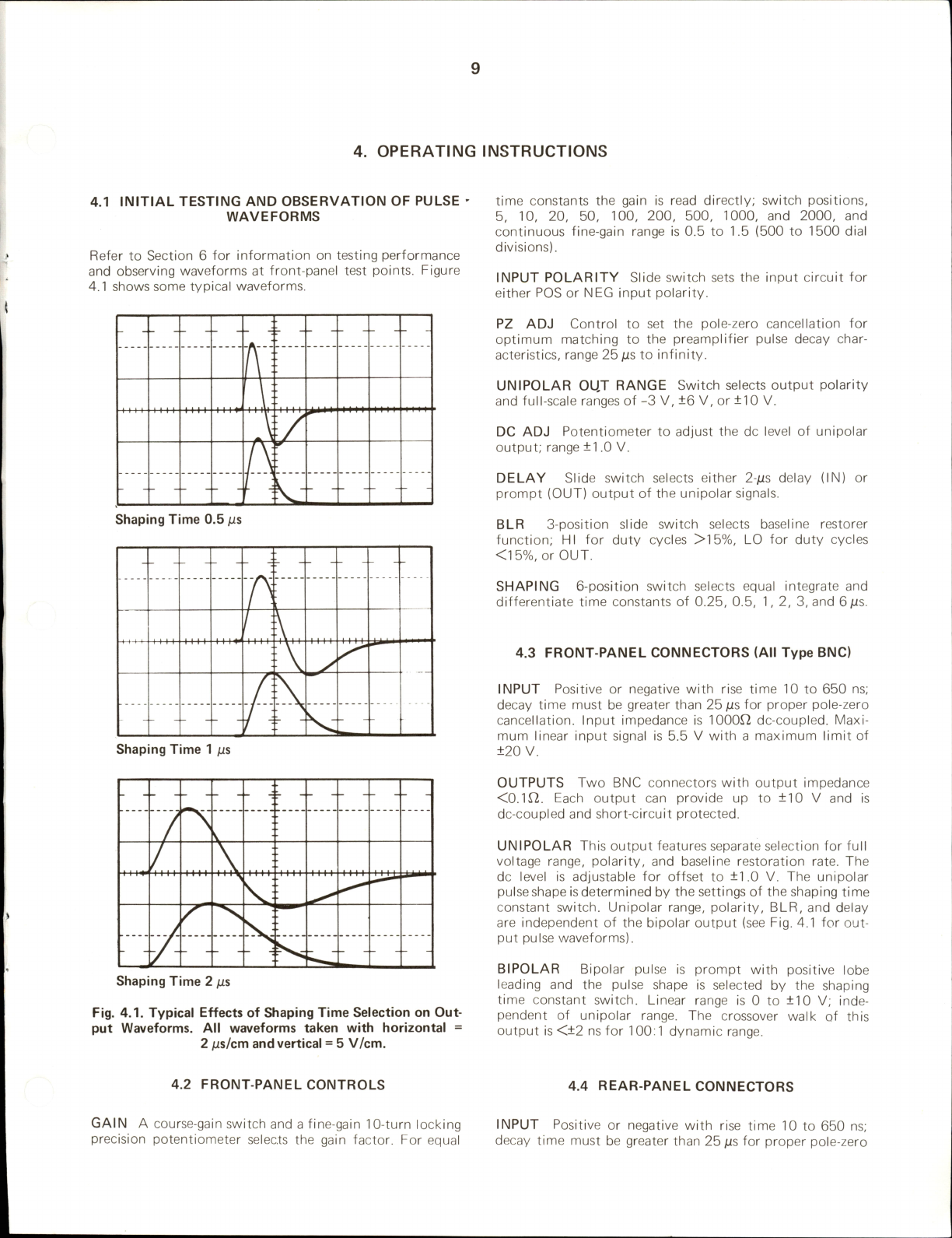
4.
OPERATING
INSTRUCTIONS
4.1
INITIAL
TESTING
AND
OBSERVATION
OF
PULSE
WAVEFORMS
Refer
to
Section
6
for
information
on
testing
performance
and
observing
waveforms
at
front-panel
test
points.
Figure
4.1
shows
some
typical
waveforms.
-
-
-
-
A
-
-
-
-
Shaping
Time
0.5
/is
Shaping
Time
1
/is
time
constants
the
gain
is
read
directly;
switch
positions,
5,
10,
20,
50,
100,
200,
500,
1000,
and
2000,
and
continuous
fine-gain
range
is
0.5
to
1.5
(500
to
1500
dial
divisions).
INPUT
POLARITY
Sl
ide
switch
sets
the
input
circuit
for
either
PCS
or
NEC
input
polarity.
PZ
ADJ
Control
to
set
the
pole-zero
cancellation
for
optimum
matching
to
the
preampl
ifier
pulse
decay
char
acteristics,
range
25
fis
to
infinity.
UNIPOLAR
OUT
RANGE
Switch
selects
output
polarity
and
ful
l-scale
ranges
of
-3
V,
±6
V,
or
±10
V.
DC
ADJ
Potentiometer
to
adjust
the
dc
level
of
unipolar
output;
range
±1.0
V.
DELAY
Sl
ide
switch
selects
either
2-/JS
delay
(IN)
or
prompt
(OUT)
output
of
the
unipolar
signals.
BLR
3-position
sl
ide
switch
selects
basel
ine
restorer
function;
HI
for
duty
cycles
>15%,
LO
for
duty
cycles
<15%,
or
OUT.
SHAPING
6-position
switch
selects
equal
integrate
and
differentiate
time
constants
of
0.25,
0.5,
1,
2,
3,
and
G/ts.
4.3
FRONT-PANEL
CONNECTORS
(All
Type
BNC)
INPUT
Positive
or
negative
with
rise
time
10
to
650
ns;
decay
time
must
be
greater
than
25/is
for
proper
pole-zero
cancel
lation.
Input
impedance
is
lOOOfi
dc-coupled.
Maxi
mum
l
inear
input
signal
is
5.5
V
with
a
maximum
l
imit
of
±20
V.
-
-
-
-
/
\
L
Shaping
Time
2
/is
Fig.
4.1.
Typical
Effects
of
Shaping
Time
Selection
on
Out
put
Waveforms.
All
waveforms
taken
with
horizontal
=
2
/is/cm
and
vertical
=
5
V/cm.
OUTPUTS
Two
BNC
connectors
with
output
impedance
<0.1^2.
Each
output
can
provide
up
to
±10
V
and
is
dc-coupled
and
short-circuit
protected.
UNIPOLAR
This
output
features
separate
selection
for
full
voltage
range,
polarity,
and
basel
ine
restoration
rate.
The
dc
level
is
adjustable
for
offset
to
±1.0
V.
The
unipolar
pulse
shape
is
determined
by
the
settings
of
the
shaping
time
constant
switch.
Unipolar
range,
polarity,
BLR,
and
delay
are
independent
of
the
bipolar
output
(see
Fig.
4.1
for
out
put
pulse
waveforms).
BIPOLAR
Bipolar
pulse
is
prompt
with
positive
lobe
leading
and
the
pulse
shape
is
selected
by
the
shaping
time
constant
switch.
Linear
range
is
0
to
±10
V;
inde
pendent
of
unipolar
range.
The
crossover
walk
of
this
output
is
<±2
ns
for
100:1
dynamic
range.
4.2
FRONT-PANEL
CONTROLS
4.4
REAR-PANEL
CONNECTORS
GAIN
A
course-gain
switch
and
a
fine-gain
10-turn
locking
precision
potentiometer
selects
the
gain
factor.
For
equal
INPUT
Positive
or
negative
with
rise
time
10
to
650
ns;
decay
time
must
be
greater
than
25/is
for
proper
pole-zero

10
cancel
lation.
Input
Impedance
is
lOOOfi
dc-coupled.
Maxi
mum
l
inear
input
signal
is
5.5
V
with
a
maximum
l
imit
of
+20
V.
OUTPUTS
The
unipolar
and
bipolar
pulses
are
brought
to,
the
rear
panel
on
BNC
connectors.
The
specifications
of
these
outputs
are
the
same
as
those
for
the
front-panel
connectors
except
that
the
output
impedance
is
93J2
at
these
connectors.
PREAMP
POWER
Standard
power
connector
for
mating
with
ORTEC
preamplifiers;
±24
V
and
±12
V.
4.5
GENERAL
CONSIDERATIONS
FOR
OPERATION
WITH
SEMICONDUCTOR
DETECTORS
Calibration
of
Test
Pulsar.
The
ORTEC
419
Pulser,
or
equivalent,
is
easily
cal
ibrated
so
that
the
maximum
pulse
height
dial
reading
(1000
divisions)
is
equivalent
to
10
MeV
loss
in
a
silicon
radiation
detector.
The
procedure
is
as
follows:
1.
Connect
the
detector
to
be
used
to
the
spectrometer
system,
i.e.,
preampl
ifier,
main
amplifier,
and
biased
anrrplifier.
2.
Allow
particles
from
a
source
of
known
energy
(alpha
particles,
for
example)
to
fal
l
on
the
detector.
3.
Adjust
the
ampl
ifier
gain
and
the
bias
level
of
the
biased
amplifier
to
give
a
suitable
output
pulse.
4.
Set
the
pulser
PULSE
HEIGHT
potentiometer
at
the
energy
of
the
alpha
particles
striking
the
detector
(e.g.,
for
a
5.47-Me\/
alpha
particle,
set
the
dial
on
547
divisions).
5.
Turn
on
the
Pulser,
and
use
the
NORMALIZE
po
tentiometer
and
attenuators
to
set
the
output
due
to
the
pulser
for
the
same
pulse
height
as
the
pulse
obtained
in
step
3.
Lock
the
NORMALIZE
dial
and
do
not
move
again
until
recal
ibration
is
necessary.
The
pulser
is
now
cal
ibrated;
the
PULSE
HEIGHT
dial
reads
in
MeV
if
the
number
of
dial
divisions
is
divided
by
100.
Amplifier
Noise
and
Resolution
Measurements.
As
shown
in
Fig.
4.2.,
the
preampl
ifier,
amplifier,
pulse
generator,
oscil
loscope,
and
a
wide-band
rms
voltmeter
such
as
the
Hewlett-Packard
400D
are
required
for
this
measurement.
Connect
a
suitable
capacitor
to
the
input
to
simulate
the
detector
capacitance
desired.
To
obtain-the
resolution
spread
due
to
ampl
ifier
noise:
/I.
Measure
the
rms
noise
voltage
(Erms)
at
the
amplifier
output.
2.
Turn
on
the
ORTEC
419
Precision
Pulse
Generator
and
adjust
the
pulser
output
to
any
convenient
readable
voltage,
Eq,
as
determined
by
the
oscilloscope.
The
full
width
at
half
maximum
spread
due
to
amplifier
noise
is
then
(FWHM)
resolution
where
E^iai
is
the
pulser
dial
reading
in
MeV,
and
2.66
is
the
factor
for
rms
to
FWHM
(2.34)
and
noise
to
rms
meter
correction
(1.13)
for
average-indicating
voltmeters
such
as
the
Hewlett-Packard
400D.
A
true
rms
voltmeter
does
not
require
the
latter
correction
factor.
Detector
Capacitor
Oscilloscope
ORTEC
Preamp
ORTEC
Amplifier
ORTEC
Pulse
Generator
Voltmeter
Fig.
4.2.
System
for
Measuring
Amplifier
and
Detector
Noise
Resolution.
The
resolution
spread
will
depend
upon
the
total
input
capacitance,
since
the
capacitance
degrades
the
signal-to-
noise
ratio
much
faster
than
the
noise.
A
typical
resolution
spread
versus
external
input
capacitance
for
the
ORTEC
120
Preampl
ifier
and
the
452
Ampl
ifier
is
shown
in
Fig.
4.3.
I
I I I
u
\
miTEC
120-2
Direct
Coupled
Shaping
T
=
2iis
14521
Direct
Coupled
Shaping
T
=
2
jjs
1452]
5
10
50
100
EXTERNAL
INPUT
CAPACITANCE
|pF)
500
1000
N(FWHM)
=
2.66
Erms
Edial
Fig.
4.3.
Resolution
Effects
of
Capacitance.

11
Detector
Noise
Resolution
Measurements.
The
same
measurement
just
described
can
be
made
with
a
biased
detector
instead
of
the
external
capacitor
used
to
simulate
the
detector
capacitance.
The
resolution
spread
wil
l
be
larger
because
the
detector
contributes
both
noise
and
capacitance
to
the
input.
The
detector
noise
resolution
spread
can
be
isolated
from
the
ampl
ifier
noise
spread
if
the
detector
capacity
is
known,
since
(Ndet)^
+
(N3rnp)
~
C^total'
'
where
Ntotal
'S
the
total
resolution
spread
and
Ngmp
is
the
amplifier
resolution
spread
with
the
detector
replaced
by
its
equivalent
capacitance.
The
detector
noise
tends
to
increase
with
bias
voltage,
but
the
detector
capacitance
decreases,
thus
reducing
the
resolution
spread.
The
overall
resolution
spread
wil
l
depend
upon
which
effect
is
dominant.
Figure
4.4
shows
curves
of
typical
total
noise
resolution
spread
versus
bias
voltage,
using
the
data
from
several
ORTEC
sil
icon
surface-barrier
semiconductor
radiation
detectors.
_
.6
111
V)
O
z
(/]
s
oc
A
-
ORTEC
B/
B
-
ORTEC
Bfi
L030-007-300
025-050-100
-025-100-100
L-030-200-100
-045-450-100
C
-ORTEC
B/
E
-ORTEC
Bfi
E
■
D
■
25
50
75
100
BIAS
VOLTAGE
125
Fig.
4.4.
Noise
as
a
Function
of
Bias
Voltage.
Amplifier
Noise
and
Resolution
Measurements
Using
a
Pulse
Height
Analyzer.
Probably
the
most
convenient
method
of
making
resolution
measurements
is
with
a
pulse
height
analyzer
as
shown
by
the
setup
il
lustrated
in
Fig.
4.5.
The
ampl
ifier
noise
resolution
spread
can
be
measured
directly
with
a
pulse
height
analyzer
and
the
mercury
pulser
as
fol
lows:
1.
Select
the
energy
of
interest
with
an
ORTEC
419
Pulse
Generator,
and
set
the
Ampl
ifier
and
Biased
Ampl
ifier
GAIN
and
BIAS
LEVEL
controls
so
that
the
energy
is
in
a
convenient
channel
of
the
analyzer.
2.
Cal
ibrate
the
analyzer
in
keV
per
channel,
using
the
pulser
(full
scale
on
the
pulser
dial
is
10
MeV
when
cal
ibrated
as
described
in
"Cal
ibration
of
Test
Pulser").
3.
Then
obtain
the
amplifier
noise
resolution
spread
by
measuring
the
FWHM
of
the
pulser
spectrum.
The
detector
noise
resolution
spread
for
a
given
detector
bias
can
be
determined
in
the
same
manner
by
connecting
a
detector
to
the
preamplifier
input.
The
amplifier
noise
resolution
spread
must
be
subtracted
as
described
in
"Detector
Noise
Resolution
Measurements".
The
detector
noise
will
vary
with
detector
size
and
bias
conditions
and
possibly
with
ambient
conditions.
ORTEC ORTEC
ORTEC
PREAMP
AMPLIFIER
1
1
1
1
AMP
DETECTOR
OR
CAPACITOR
ORTEC
PULSE
GENERATOR
ORTEC
444
GATED
BIASED
AMPUFIER
MULTICHANNEL
PULSE
HEIGHT
ANALYZER
ORTEC
PULSE
STRETCHER
Fig.
4.5.
System
for
Measuring
Resolution
with
a
Pulse
Height
Analyzer.
Current-Voltage
Measurements
for
Silicon
and
Germanium
Detectors.
The
ampl
ifier
system
is
not
directly
involved
in
semiconductor
detector
current-voltage
measurements,
but
the
ampl
ifier
serves
well
to
permit
noise
monitoring
during
the
setup.
The
detector
noise
measurement
is
a
more
sensitive
method
of
determining
the
maximum
detector
voltage
which
should
be
used,
because
the
noise
increases
more
rapidly
than
the
reverse
current
at
the
onset
of
detector
breakdown.
Make
this
measurement
in
the
absence
of
a
source.
Figure
4.6
shows
the
setup
required
for
current-voltage
measurements.
The
ORTEC
428
Bias
Supply
is
used
as
the
voltage
source.
Bias
voltage
should
be
appl
ied
slowly
and
reduced
when
noise
increases
rapidly
as
a
function
of
applied
bias.
Figure4.7
shows
several
typical
current-voltage
curves
for
ORTEC
silicon
surface-barrier
detectors.
VTVM
CURRENT
MONITORINO
JACKS
DETECTOR
r-
BYPASS
CAPACITOR
DETECTOR
BIAS
SUPPLY
ORTEC
AMPLIFIER
ORTEC
PREAMPLIFIER
ORTEC
RMS
VOLTMETER
MICRO-
AMMETER
Fig.
4.6.
System
for
Detector
Current
and
Voltage
Measurements.

12
<
.40
h-
III
.30
CC
.20
-)
o
u
10
<
CD
0
A
-
ORTEC
BA-030-007
300
B
-
ORTEC
BA-025-050-100
C
-
ORTEC
BA-025-100-100
D
-
ORTEC
BA
030-200-100
E
-
ORTEC
BA-045-450-100
E
D
R
C
A
50
70
90
BIAS
VOLTAGE
110
Fig.
4.7.
Silicon
Detector
Back
Current
vs
Bias
Voltage.
When
it
is
possible
to
float
the
microammeter
at
the
detector
bias
voltage,
the
method
of
detector
current
measurement
shown
by
the
dashed
l
ines
in
Fig.
4.6
is
preferable.
The
detector
is
grounded
as
in
normal
operation
and
the
microammeter
is
connected
to
the
current
moni
toring
jack
on
the
428
Detector
Bias
Supply.
Preamplifier—Main
Amplifier
Gain
Adjustments
as
a
Func
tion
of
Input
Particle
Energy.
With
the
input
energy
at
a
constant,
or
maximum,
known
value,
the
fol
lowing
method
is
recommended
for
adjusting
the
total
system
gain
of
the
preamplifier
and
main
amplifier
to
an
optimum
value.
1.
The
primary
design
criterion
for
the
preampl
ifier
is
the
best
signal-to-noise
ratio
at
the
output;
therefore
the
preamplifier
should
be
operated
with
the
gain
switch
in
its
maximum
gain
position.
This
will
result
in
the
best
signal-to-noise
ratio
available,
and
at
the
same
time
the
absolute
voltage
ampl
itude
of
the
preampl
ifier
signal
will
be
maximized.
2.
Since
the
fine-gain
control
of
the
452
is
an
attenuator,
it
should
be
set
to
as
near
maximum
as
possible
by
manipula
tion
of
the
coarse
gain.
3.
The
unipolar
output
range
should
be
set
to
the
input
range
of
the
analyzer.
4.6
OPERATION
IN
SPECTROSCOPY
SYSTEMS
High-Resolution
Alpha-Particle
Spectroscopy
System.
The
block
diagram
of
a
high-resolution
spectroscopy
system
for
measuring
natural
alpha-particle
radiation
is
shown
in
Fig.
4.8.
Since
natural
alpha-particle
radiation
only
occurs
above
several
MeV,
an
ORTEC
444
Biased
Ampl
ifier
is
used
to
suppress
the
unused
portion
of
the
spectrum.
Alpha-
particle
resolution
is
obtained
in
the
following
manner:
1.
Using
maximum
preampl
ifier
gain,
medium
amplifier
gain,
and
minimum
biased
ampl
ifier
gain
and
bias
level,
accumulate
the
alpha
peak
in
the
multichannel
analyzer.
2.
Slowly
increase
the
bias
level
and
biased
ampl
ifier
gain
until
the
alpha
peak
is
spread
over
5
to
10
channels
and
the
minimum
to
maximum
energy
range
desired
corresponds
to
the
first
and
last
channels
of
the
analyzer.
3.
Cal
ibrate
the
analyzer
in
keV
per
channel
using
the
pulser
and
the
known
energy
of
the
alpha
peak
(see
"Cal
ibration
of
Test
Pulses"),
or
two
known
energy
alpha
peaks.
4.
The
resolution
can
be
obtained
by
measuring
the
FWFIIVI
of
the
alpha
peak
in
channels
and
converting
to
keV.
MVTM
OMTM
Priaip
n
Llaiar
fa
iplifMr
Biasatf
Aiiplitilt
1
ewTBe
Dctictif
Bias
Sapphr
1
1
OWTM
Pflsa
CMtratw
—
0
0
$ctpt
N«iSt
MitH
llilticliMid
Nhe
Htiftt
Aialy^if
Fig.
4.8.
System
for
High-Resolution
Alpha-Particle
Spectroscopy.
High-Resolution
Gamma
Spectroscopy
System.
A
high-
resolution
gamma
system
block
diagram
is
shown
in
Fig.
4.9.
Although
a
biased
ampl
ifier
is
not
shown
(a
larger
channel
analyzer
being
preferred),
it
can
be
used
if
only
a
smaller
channel
analyzer
is
available
and
only
higher
energies
are
of
interest.
When
using
lithium-drifted
germanium
detectors
cooled
by
a
liquid-nitrogen
cryostat,
it
is
possible
to
obtain
resolutions
from
about
1
keV
FWHM
up
(depending
on
the
energy
of
the
incident
radiation
and
the
size
and
qual
ity
of
the
detector).
Reasonable
care
is
required
to
obtain
such
results.
Some
guide
l
ines
for
obtaining
optimum
resolution
are:
1.
Keep
interconnection
capacities
between
the
detector
and
preamplifier
to
an
absolute
minimum
(no
cables).
2.
Keep
humidity
low
near
the
detector-preamplifier
junction.
3.
Operate
in
ampl
ifier
and
preampl
ifier
gain
regions
which
provide
the
best
signal-to-noise
ratio.
4.
Operate
at
the
highest
al
lowable
detector
bias
to
keep
the
input
capacity
low.
ORTEC
DETECTOR
BIAS
SUPPLY
ORTEC
PREAMPLIFIER
2000
-
8000
CHANNEL
PULSE
HEIGHT
ANALYZER
/Li
Drift
Detector
a
\
Cryostat
ORTEC
©
0
PULSE
GENERATOR
SCOPE
NOISE
METER
Fig.
4.9.
System
for
High-Resolution
Gamma
Spectroscopy.
Scintillation
Counter
Gamma
Spectroscopy
Systems.
The
ORTEC
452
can
be
used
in
scintil
lation
counter
spectros
copy
systems
as
shown
in
Fig.
4.10.
The
ampl
ifier
clipping
time
constants
should
be
selected
in
the
region
of
0.5
to
1.0;usfor
Nal
or
plastic
scintil
lators.
For
scintillators
having
longer
decay
times,
longer
time
constants
should
deselected.

13
High
Voltage
Scintillation
Counter
ORTEC
Scintillation
Counter
Preamp
ORTEC
Pulse
Generator
ORTEC
Amplifier
Multichannel
-
Pulse
Height
Analyzer
Fig.
4.10.
Scintillation
Counter
Gamma
Spectroscopy
System.
X-Ray
Spectroscopy
Using
Proportional
Counters.
Space
charge
effects
in
proportional
counters
operated
at
high
gas
ampl
ification
tend
to
degrade
the
resolution
capabil
ities
drastically
at
x-ray
energies,
even
at
relatively
low
counting
rates.
By
using
a
high-gain
low-noise
amplifying
system
and
lower
gas
ampl
ification,
these
effects
can
be
reduced
and
a
considerable
improvement
in
resolution
can
be
obtained.
The
block
diagram
in
Fig.
4.11
shows
a
system
of
this
type.
Analysis
can
be
accomplished
by
simultaneous
acquisition
of
all
data
on
a
multichannel
analyzer
or
counting
a
region
of
interest
in
a
single
channel
analyzer
window
with
a
sealer
and
timer
or
counting
rate
meter.
ORTEC
High
Voltage
Supply
ORTEC
Single
Channel
Analyzer
^
Counting
Rate
Meter
or
Sealer
&
Timer
P
Proportional
Counter
ORTEC
Proportional
Counter
Preamp
Pulse
Generator
ORTEC
Amplifier
Multichannel
Pulse
Height
Analyzer
Fig.
4.11.
High-Resolution
X-Ray
Energy
Analysis
System.
4.7
OTHER
EXPERIMENTS
Block
diagrams
illustrating
how
the
452
and
other
ORTEC
400
Series
modules
can
be
used
in
experimental
setups
are
given
in
Figs.
4.12—4.15.
Attirnatii
P.M.
Base
ITubi
Nal
Time
Pickott
emrae
enrae enrae enrae
Scintillation
Ampiifior
Timing
SInglo
Channol
Analyzir
1
Timo
Pickoff
Proamp
1
i
Unit
#
Source
cp
6e
Li-Crifted
Detector
onrae
Preamp
Fast
Coincidence
Unit
enrao
453
Constant
/
Timing
Discriminator
1
t
enrae
Gate
&
Dolay
Ganirator
t
1
enrae
1
enrae
liniar
Gate
Linear
Output
ti
Multichannol
454
Tlmint
Fitter
Amplifier
Analyzer
Amplifier
Delay
Amplifier
Fig.
4.12.
Gamma-Gamma
Coincidence
Experiment.
onrae
Preamp
onrac
Amplifier
OMTac
Tlmlnp
Single
ChaMel
Anahizer
I
enrae
Time
Pickoff
Centrol
Tine
PIckeff
Unit
Silicon
Surface
-.Barrier
Detector
#
Source
up
LiDrifted
Germanium
Detector
Preamp
—
--
—
"
f
onr
Bc
454
Censtant
/
Timing
Discrjmieatnr
1
i
onrac
Tlmmg
Filter
Amplifier
1
1
Gate
1
Delay
Generator
onraconrac
Fast
Coincidence
—
Linear
Gate
Unit
Amplifier
Delay
Amplifier
Linear
Output
toMuIti
Channel
Analyzer
Fig.
4.13.
Gamma-Ray
Charged-Particle
Coincidence
Experiment

14
Fist
Coincidinci
Unit
Timini
Flltir
Amplitiir
Liniir
6ati
Diliy
Amplitiir
Timi
Pickoff
Control
Goto
A
Delay
Ganirator
Constant
/
Timing
Oiscriminatir
Amplitiir
Tiffli
Pickott
Unit
Amplitiir
Priamp
P.I1I.
Tubi
I
Basi
Nal
Fig.
4.14.
Gamma-Ray
Pair
Spectrometer.
□
RTEC
Preamp
A.
Enerey
Gated
Multichannel
Pulse
Height
Analyzer
Linear
Gate
or
Gated
Biased
Amplifier
Unipol
Amplifier
BiDOlar
S
C
A
for
E
T
Pichott
□
RTEC
Preamp
□RTEC
I
Amplifier
ORTEC
Delay
ORTEC
Linear
Gate
or
Gated
Biased
Amplifier
B.
Time
Gated
Other
Gating
Signals
S
C
A
or
E
T
P
choff
ORTEC:
Coincidence
Multichannel
Pulse
Height
Analyzer
Fig.
4.15.
General
System
Arrangement
for
Gating
Control.
4.8
BASELINE
RESTORER
(BLR)
Function
DC
Level.
The
operation
of
the
452
in
the
system
is
quite
straightforward.
The
Output
Range
Switch
selects
the
span
of
the
output
voltage
to
be
-3
V,
±6
V,
or
±10
V
for
the
Unipolar
Output.
This
allows
a
matching
to
all
ADC
inputs.
On
some
ADC's
the
input
has
a
zero
offset
adjust
to
set
the
zero
channel
intercept
which
controls
a
dc
level
internally
in
the
ADC,
normal
ly
operating
in
the
ac-coupled
mode;
however,
when
direct
access
is
used,
this
dc
offset
adjust
is
to
some
degree
disabled
by
the
output
impedance
of
the
driving
amplifier
(in
this
case,
the
452
which
controls
the
amount
of
that
dc
voltage).
Since
the
452
dc
output
level
controls
the
zero
intercept
of
these
ADC's,
this
dc
level
is
front-panel
adjustable
between
+1.0
V
and
-1.0
V.
The
manual
for
the
ADC
used
should
be
referred
to
for
determining
the
desired
dc
level.
Controls.
The
BLR
rate
switch
(S4)
has
three
positions.
Out,
Lo,
and
Hi,
and
selects
the
rate
of
dc
restoration.
The
Out
mode
is
used
when
the
count
rate
is
low
to
moderate
and
best
energy
resolution
(the
least
noise
width
contri
bution)
is
required.
In
many
experimental
systems
the
Lo
position
of
the
BLR
switch
may
give
better
results
than
the
Out
position,
even
at
low
count
rates.
This
wil
l
especially
be
true
if
the
system
is
microphonic
or
a
ground
loop
exists.
The
Lo
and
Hi
restore
modes
provide
a
selectable
restoration
rate
and
therefore
a
very
much
higher
count
rate
capabil
ity
for
the
same
amount
of
pileup
distortion.
The
restorer
should
be
used
whenever
high
count
rates
(approximately
5000
to
10,000
counts/sec)
are
to
be
encountered.
BLR
switch
selects
the
restorer
capacitor
to
al
low
optimum
restoration
for
each
range
of
count
rates,
or
bypasses
the
BLR
when
it
is
set
at
Out.
(See
Fig.
4.16
for
aid
in
selection
of
the
best
BLR
rate.)
A
BIR
Out
T-1
us
□
BLR
High
T-1
us
O
BLR
lo«
T-1
us
COUNTS
PTR
SECOND
Fig.
4.16.
Effects
of
Baseline
Restorer
on
Resolution.
Used
in
a
System
If
the
452
is
used
in
a
system
that
also
includesa
nonl
inear
element
such
as
a
biased
amplifier,
the
system
must
be
dc-coupled
up
to
the
nonl
inear
element
or
be
dc-restored
prior
to
it
in
order
to
obtain
good
pulse
height
resolution.
If
the
output
from
the
nonlinear
element
is
ac-coupled,
dc
restoration
is
required
again
before
the
pulses
are
fed
into
a
pulse
height
analysis
system
(multichannel
analyzer,
for
example)
to
obtain
the
best
pulse
height
resolution
versus
count
rate.
These
precautions
are
satisifed
by
using
an
ORTEC
444
Biased
Ampl
ifier
at
moderate
count
rates,
since
it
contains
a
dc
restoration
circuit.
Of
course,
it
is
necessary
to
have
dc
coupl
ing
fol
lowing
the
dc
restoration
through
to
the
pulse
height
analysis
system.
Some
of
the
analog-to-digital
converters
associated
with
multichannel
analyzers
are
not
dc-coupled
at
their
normal

15
input
and
contain
no
method
of
dc
restoration;
however,
some
of
these
analyzers
do
allow
direct
access
to
their
linear
gate
circuitry
in
the
so-called
Mossbauer
analysis
mode.
Other
ADC's
have
a
built-in
dc
restorer
capable
of
restoring
the
long
time
constant
associated
with
the
ac-coupl
ing
capacitor
in
the
ADC
prior
to
the
dc
restorer
point.
In
these
cases,
one
may
obtain
a
reasonably
high
count
rate,
i.e.,
of
the
order
of
10,000
to
15,000
counts/sec,
of
high-resolution
data
by
dc
restoration
externally
and
coupling
directly
into
the
ADC
in
the
normal
mode.
This
means
that
there
are
two
steps
of
dc
restoration.
If,
however,
very
high
count
rates
are
to
be
encountered,
one
should
assure
dc
coupling
in
these
ADC's
as
well
and
dc
restoration
externally
by
means
of
the
452.
4.9
METHODS
OF
CONNECTION
TO
VARIOUS
ANALYZERS
There
are
many
ADC's
in
use
in
nuclear
research
and
the
variety
of
input
requirements
is
almost
as
broad
as the
variety
of
ADC's
used.
The
ADC's
l
isted
below
and
the
block
diagrams
of
Figs.
4.17
and
4.18
outline
methods
of
con
necting
the
452
into
the
system
in
such
a
way
that
it
will
perform
its
function
and
supply
an
analysis
signal
to
the
ADC
through
a
dc-coupled
network.
Note
that
in
some
cases
it
is
necessary
to
feed
two
signals
to
the
ADC.
One
of
these,
which
is
the
dc-coupled
signal
to
be
analyzed,
goes
directly
to
the
gate
circuit,
while
the
second
signal
goes
to
the
normal
input
and
is
used
merely
as
a
trigger
signal
to
initiate
analysis
since
some
of
the
ADC's
pick
off
the
trig
ger
signal
to
initiate
analysis
from
the
normal
(0
to
10
V)
input.
Various
manufacturers
of
multichannel
analyzers
and
their
recommended
method
of
dc
coupling
of
specific
ADC's
are
given
below.
Figure
4.17
appl
ies
when
no
trigger
is
needed,
and
Fig.
4.18
appl
ies
when
an
external
trigger
is
indicated.
If
information
in
excess
of
that
given
is
necessary,
contact
the
analyzer
manufacturers
for
further
details.
A.
RIDL
(NUCLEAR-CHICAGO)
Models
34-12B,
34-27,
22-Series.
PACKARD
INSTRUMENTS
INTERTECHNIQUE
Direct
access
available
through
the
dc
or
Mossbauer
Input
(trigger
required).
B.
NORTHERN
SCIENTIFIC
Direct
access
available
on
all
models
(no
trigger
required)
.
C.
NUCLEAR
DATA
ADC
Direct
Input
Modification
Trigger
Condition
ND-120
-3
ND-130
-3
Short
out
0.01-
juF
capacitor
on
ADC
board,
base
of
T-1
None
Req.
ND-110
-2.5
None
(use
Moss
bauer
Input)
None
Req.
ND-160F
-3
None
(use
Direct)
None
Req.
ND-161F
-3
Short
out
0.018-
/LiF
capacitor
on
ADC
board,
base
of
T-1
None
Req.
ND-2200
0-5
Short
out
capaci-
(offset
base-
tor
09D8
on
line)
board
No
trigger
required
if
operated
in
open
gate
ND-3300
+10
Short
out
0.01-
;uF
capacitor
on
ALG
board
Trigger
required
D.
TMC
ANALYZER
QUIREMENTS
AND
ADC
DIRECT
INPUT
RE-
Model
No.
Signal
Required
(V)
Modifications
102
Analyzer
213
ADC
0
to
-4
0
to
+8
Yes^
Yes'^
401
D
Analyzer
0
to
-4
Yes®
404C
Analyzer
o
0
1
tip-
Yes®
461
ADC
O
0
1
CO
No
1001
Analyzer
0
to
-4
Yes®
1004
Analyzer
0
to
-4
Yes®
1010
Analyzer
1
o
o
Yes®
217B
ADC
0
to
-4
Yes®
®Add
signal
input
and
trigger
input
for
Linear
Gate.
bAdd
signal
input
and
special
trigger
input.
CAdd
signal
input
to
Linear
Gate
circuit.
E.
TU
LLAMORE
(Victoreen)
signal
0
to
-i-10
V
Model
No.
Modification
Trigger
dc
Level
(V)
PIP-400
Short
C-203
None
~+1.5
SCIPP
Series
Short
C-403
None
~+1.5
ICADC
None None
~
0
Si9nal
(Positfve
Of
Ne9siN«)
OPTEC
Pos
or
Neg
*
D
C
tffljillfier
Direct
Input
700334
Shaping
Amplifier
With
Baseline
Restorer
iPositive
or
Ne9ativ
OPTEC
or
Delaved
Pos
or
Neq
D
C
or
Amplifier
Unipolar
«
D
C
200336
Normat
Input
L
Bipolar
Fig.
4.17.
Analyzer
Connection
with
No
Trigger
Required.
Fig.
4.18.
Analyzer
Connection
When
Trigger
Is
Required.
Table of contents
Other EG&G Amplifier manuals

EG&G
EG&G 113 Service manual

EG&G
EG&G ORTEC 427 User manual

EG&G
EG&G ORTEC 474 Service manual

EG&G
EG&G ORTEC 575A Service manual

EG&G
EG&G ORTEC 414A Service manual

EG&G
EG&G ORTEC 485 User manual

EG&G
EG&G ORTEC 444 User manual

EG&G
EG&G ORTEC 113 Service manual

EG&G
EG&G ORTEC 572 Service manual

EG&G
EG&G ORTEC 118A User manual


