EG&G ORTEC 414A Service manual

A.
A-
I
.
^
Model
414A
Fast
Coincidence
Operating
and
Service
Manual
J
Model
414A
Fast
Coincidence
Operating
and
Service
Manual
This
manual
applies
to
instruments
marked
"Rev
19"
on
rear
panel
Printed
in
U.S.A.
2880
0.5C
0580
STANDARD
WARRANTY
FOR
EG&G
ORTEC
INSTRUMENTS
EG&G
ORTEC
warrants
that
the
items
will
be
delivered
free
from
defects
in
material
or
workmanship.
EG&G
ORTEC
makes
no
other
warranties,
express
or
implied,
and
specifically
NO
WARRANTY
OF
MERCHANTABILITY
OR
FITNESS
FOR
A
PARTICULAR
PURPOSE.
EG&G
ORTEC's
exclusive
liability
is
limited
to
repairing
or
replacing
at
EG&G
ORTEC's
option,
items
found
by
EG&G
ORTEC
to
be
defective
in
workmanship
or
materials
within
one
year
from
the
date
of
delivery.
EG&G
ORTEC's
liability
on
any
claim
of
any
kind,
including
negligence,
loss
or
damages
arising
out
of,
connected
with,
or
from
the
performance
or
breach
thereof,
or
from
the
manufacture,
sale,
delivery,
resale,
repair,
oruseof
any
item
or
services
covered
by
this
agree
ment
or
purchase
order,
shall
in
no
case
exceed
the
price
allocable
to
the
item
or
service
furnished
or
any
part
thereof
that
gives
rise
to
the
claim.
In
the
event
EG&G
ORTEC
fails
to
manufacture
or
deliver
items
called
for
in
this
agreement
or
purchase
order,
EG&G
ORTEC's
exclusive
liability
and
buyer's
exclusive
remedy
shall
be
release
of
the
buyer
from
the
obligation
to
pay
the
purchase
price.
In
no
event
shall
EG&G
ORTEC
be
liable
for
special
or
consequential
damages.
QUALITY
CONTROL
Before
being
approved
for
shipment,
each
EG&G
ORTEC
instrument
must
pass
a
stringent
set
of
quality
control
tests
designed
to
expose
any
flaws
in
materials
or
workmanship.
Permanent
records
of
these
tests
are
maintained
for
use
in
warranty
repair
and
as
a
source
of
statistical
information
for
design
improvements.
REPAIR
SERVICE
If
it
becomes
necessary
to
return
this
instrument
for
repair,
it
is
essential
that
Customer
Services
be
contacted
in
advance
of
its
return
so
that
a
f^eturn
Authorization
Number
can
be
assigned
to
the
unit.
Also,
EG&G
ORTEC
must
be
informed,
either
in
writing
or
by
telephone
[(615)
482-4411],
of
the
nature
of
the
fault
of
the
instrument
being
returned
and
of
the
model,
serial,
and
revision
("Rev"
on
rear
panel)
numbers.
Failure
to
do
so
may
cause
unnecessary
delays
in
getting
the
unit
repaired.
The
EG&G
ORTEC
standard
procedure
requires
that
instruments
returned
for
repair
pass
the
same
quality
control
tests
that
are
used
for
new-production
instruments.
Instruments
that
are
returned
should
be
packed
so
that
they
will
withstand
normal
transit
handling
and
must
be
shipped
PREPAID
via
Air
Parcel
Post
or
United
Parcel Service
to
the
nearest
EG&G
ORTEC
repair
center.
The
address
label
and
the
package
should
include
the
Return
Authorization
Number
assigned.
Instruments
being
returned
that
are
damaged
in
transit
due
to
inadequate
packing
will
be
repaired
at
the
sender's
expense,
and
it
will
be
the
sender's
responsibility
to
make
claim
with
the
shipper.
Instruments
not
in
vvarranty
will
be
repaired
at
the
standard
charge
unless
they
have
been
grossly
misused
or
mishandled,
in
which
case
the
user
will
be
notified
prior
to
the
repair
being
done.
A
quotation
will
be
sent
with
the
notification.
DAMAGE
IN
TRANSIT
Shipments
should
be
examined
immediately
upon
receipt
for
evidence
of
external
or
concealed
damage.
The
carrier
making
delivery
should
be
notified
immediately
of
any
such
damage,
since
the
carrier
is
normally
liable
for
damage
in
shipment.
Packing
materials,
waybills,
and
other
such
documentation
should
be
preserved
in
order
to
establish
claims.
After
such
notification
to
the
carrier,
please
notify
EG&G
ORTEC
of
the
circumstances
so
that
assistance
can
be
provided
in
making
damage
claims
and
in
providing
replacement
equipment
if
necessary.
Ill
CONTENTS
Page
WARRANTY
PHOTOGRAPH
1.
DESCRIPTION
,
2.
SPECIFICATIONS
I
2.1.
Performance
2.2.
Controls
'
*
'
2.3.
Inputs
!
''
'
2
2.4.
Outputs
•
•
..
.
^
2.5.
Electrical
and
Mechanical
[[
'
2
3.
INSTALLATION
2
3.1.
General
Installation
Considerations
2
3.2.
Connection
to
Power
^
3.3.
Logic
Inputs
to
the
Fast
Coincidence
.
2
4.
OPERATING
INSTRUCTIONS
3
4.1.
Front
Panel
Controls
,
,
3
4.2.
Testing
and
Observation
of
Waveforms
3
4.3.
Connector
Data
''''
3
4.4.
Typical
Operating
Considerations
3
5.
CIRCUIT
DESCRIPTION
4
6.
MAINTENANCE
5
6.1.
Testing
Performance.
.:
5
6.2.
Alignment
of
Resolving
Time
Trimmer
Capacitors
5
6.3.
Suggestions
for
Troubleshooting
.
!!
!
!
.'
6
6.4.
Tabulated
Test
Point
Voltages
on
Etched
Board
7
Replaceable
Parts
List
Block
Diagram
and
Schematics
414A-0101-B1
414A-0164-S1
ILLUSTRATIONS
Fig.
4.1.
Illustration
of
Actual
Overlapping
of
Input
Pulses
I
and
II,
but
Not
During
the
Leading-Edge
Resolving
Time;
Trace
III
Illustrates
No
Output
Pulse
3
Fig.
4.2.
Illustration
of
Input
Pulses
I
and
II
Overlapping
During
the
Leading-Edge
Resolving
Time
and
Producing
Output
Pulse
III
3
Fig.
6.1.
414A
Test
and
Calibrate
Circuit
5
*
'»
i
\
.
1
on>o^!
U
?
-
»»
'i
\
A1

ORTEC
414A
FAST
COINCIDENCE
1.
DESCRIPTION
The
414A
Fast
Coincidence
allows
fast
coincidence
determination
between
any
two
or
three
input
signals.
A
dc-coupled
anticoincidence
input
is
provided
to
inhibit
the
coincidence
output.
The
coincidence
output
can
be
inhibited
by
a
dc
voltage
or
a
pulse
that
overlaps
the
period
of
coincidence
of
the
coincident
pulses.
The
resolving
time
of
the
anticoincidence
circuit
is
set
by
the
width
of
the
input
pulse.
The
resolving
time
(2t)
of
the
Fast
Coincidence
unit
may
be
varied
over
a
10-
to
110-nsec
range
by
a
10-turn
control
for
accurate
resettability
of
the
resolving
time.
All
four
inputs
are
controlled
by
In/Out
toggle
switches.
Input
signal
requirements
are
compatible
with
NIM
slow
positive
logic
output
signals
of
a
variety
of
ORTEC
timing
equipment.
The
output
pulse
is
suitable
as
an
input
to
the
418A
Universal
Coincidence
module
and
other
modules
of
the
ORTEC
400
Series
requiring
a
logic
input
pulse.
The
module
obtains
the
necessary
operating
power
from
an
ORTEC
401/402
Series
Bin
and
Power
Supply.
The
output
signal
and
all
signal
inputs
use
front
panel
BNC
connectors.
The
instrument
is
designed
to
meet
the
recommended
interchangeability
standards
outlined
in
USAEC
Report
TID-20893
(Rev).
An
ORTEC
401/402
Bin
and
Power
Supply
provides
all
necessary
power
through
the
rear
module
connector.
All
signal
levels
and
impedances
are
compatible
with
other
modules
in
the
ORTEC
400
Series.
The
414A
is
basically
a
threefold
AND
circuit,
with
each
input
to
the
AND
circuit
regenerated,
or
reshaped,
to
a
standardized
waveform
in
passing
from
the
input
connector
to
the
actual
AND
circuit.
The
general
connotation
of
the
word
"fast"
tends
to
be
in
terms
of
elapsed
time
or
speed,
but
in
this
instrument
the
term
"fast"
is
actually
intended
to
indicate
the
general
nature
of
the
coincidence
circuit;
i.e.,
the
input
pulses
are
reshaped
and
the
actual
coincidence
determination
is
made
on
the
leading
edge,
or
leading
portion,
of
the
input
pulses.
The
three
coincidence
inputs
to
the
414A-
feed
into
identical
but
separate
shaper
circuits.
The
shaper
circuit
contains
a
voltage
limiter
to
allow
a
wide
dynamic
range
of
input
pulse
amplitudes.
The
output
of
the
limiter
feeds
into
a
regeneration
circuit,
where
a
standard
pulse
is
generated
for
each
input
pulse
regardless
of
the
actual
waveform
of
the
input
signal.
This
standard
pulse
is
then
fed
into
the
resolving
time
network,
where
it
is
reshaped
to
satisfy
the
2r
resolving
time
selected
via
the
front
panel
Resolving
Time
control.
The
outputs
of
the
three
resolving
time
networks
are
fed
in
parallel
to
an
"overlap"
coincidence
network,
i.e.,
an
AND
network.
When
portions
of
the
reshaped
input
pulses
overlap
each
other,
the
AND
circuit
recognizes
a
coincidence
event
within
the
resolving
time
set
on
the
front
panel
Resolving
Time
control
and
produces
an
output.
The
coincidence
recognition
output
from
the
AND
circuit
may
be
inhibited
by
a
signal
from
the
anticoincidence
input.
This
inhibit
signal
may
be
a
pulse
or
a
dc
voltage
since
the
anticoincidence
circuit
is
dc-coupled.
The
inhibit
period
is
determined
by
the
width
of
the
input
pulse.
If
the
output
from
the
AND
circuit
is
not
blocked
by
the
anticoincidence
circuit,
it
is
regenerated
into
a
standard
output
signal
from
the
414A,
indicating
that
a
coincidence
event
has
been
detected.
The
coincidence
inputs
are
controlled
by
front
panel
toggle
switches,
which
permit
selection
of
one-,
two-,
or
threefold
coincidence.
A
switch
is
also
provided
for
the
anticoincidence
input.
These
switches
allow
each
input
to
be
disabled
without
the
associated
coaxial
cable
having
to
be
removed.
2.
SPECIFICATIONS
2.1.
PERFORMANCE
2.2.
CONTROLS
Pulse
Pair
Resolution
<100
nsec
on
any
single
input;
for
coincidence
events,
<1
psec
on
the
coincidence
output.
Resolving
Time
(2r)
Continuously
variable
from
10
to
110
nsec
for
coincidence
signals;
set
by
the
width
of
the
input
pulse
for
the
anticoincidence
signal.
Temperature
Instability
2t
changes
<0.2%/°C,
0
to
50°C.
Resolving
Time,
10-110
nsec
Front
panel
10-turn
poten
tiometer
for
controlling
resolving
time
for
inputs
A,
B,
and
C
over
a
range
of
10
to
110
nsec.
In/Out
Toggle
switches
for
using
any
input
combination
desired
and
for
disabling
input
signals
to
the
coincidence
and
anticoincidence
circuits
without
input
coaxial
cables
having
to
be
removed.
2.3.
INPUTS
Coinc
Front
panel
BNC
connectors
provide
3
ac-coupled
coincidence
inputs
(A,B,C)
of
positive
polarity;
2-V
threshold,
20-nsec
minimum
width
required;
absolute
maximum
input
50
V;
impedance
>300Qfi.
Anticoinc
Front
panel
BNC
connector
provides
one
dc-coupled
anticoincidence
input
(D)
for
inhibiting
coincidence
output;
+2-V
threshold,
20-nsec
minimum
width
required;
absolute
max
input
50
V;
impedance
>3000n.
2.4.
OUTPUTS
Outputs
Two
seperate
buffered
coincidence
output
signals
through
BNC
connectors
on
front
panel
provide
positive
pulses
500
nsec
wide
with
5-V
minimum
amplitude;
ac-coupled
with
<10^2
impedance;
monitored
through
oscilloscope
test
points
on
front
panel.
2.5.
ELECTRICAL
AND
MECHANICAL
Power
Required
+24
V,
30
mA;
-24
V,
30
mA;
+
12
V,
120
mA;-12
V,
85
mA.
Weight
(Shipping)
4.4
lb
(2.0
kg).
Weight
(Net)
2.4
lb
(1.09
kg).
Dimensions
NIM-standard
double-width
module
(2.70
by
8.714
in.)
per
TID-20893
(Rev).
3.
INSTALLATION
3.1.
GENERAL
INSTALLATION
CONSIDERATIONS
The
414A
contains
no
internal
power
supply
but
is
used
in
conjunction
with
a
401/402
Series
Bin
and
Power
Supply,
which
is
intended
for
rack
mounting.
Therefore,
if
vacuum
tube
equipment
is
operated
in
the
same
rack,
there
must
be
sufficient
cooling
air
circulating
to
prevent
any
localized
heating
of
the
all-transistor
circuitry
used
throughout
the
414A.
The
temperature
of
equipment
mounted
in
racks
can
easily
exceed
the
recommended
maximum
unless
precautions
are
taken;
the
414A
should
not
be
subjected
to
temperatures
in
excess
of
120°F
(50°C).
must
be
given
to
ensure
that
reflections
in
the
driving
transmission
cable
do
not
occur.
There
are
three
general
methods
of
termination
that
are
used.
The
simplest
of
these
is
shunt
termination
at
the
receiving
end
of
the
cable.
A
second
method
is
series
termination
at
the
sending
end.
The
third
is
a
combination
of
series
and
shunt
termination,
where
the
cable
impedance
is
matched
both
in
series
at
the
sending
end
and
in
shunt
at
the
receiving
end.
The
most
effective
method
is
the
combination,
but
termination
by
this
method
reduces
the
amount
of
signal
strength
at
the
receiving
end
to
50%
of
that
which
is
available
in
the
sending
instrument.
3.2.
CONNECTION
TO
POWER
Turn
off
the
Bin
power
supply
when
inserting
or
removing
modules.
The
ORTEC
400
Series
is
designed
so
that
it
is
not
possible
to
overload
the
Bin
power
supply
with
a
full
complement
of
modules
in
the
Bin.
Since,
however,
this
may
not
be
true
when
the
Bin
contains
modules
other
than
those
of
ORTEC
design,
the
Power
Supply
voltages
should
be
checked
after
the
modules
are
inserted.
The
401/402
has
test
points
on
the
Power
Supply
control
panel
to
monitor
the
dc
voltages.
3.3.
LOGIC
INPUTS
TO
THE
FAST
COINCIDENCE
The
input
pulses
to
the
Fast
Coincidence
unit
may
come
from
any
source
of
logic
pulses.
The
input
impedance
of
the
Fast
Coincidence
is
greater
than
3000f2,
and
some
care
To
use
shunt
termination
at
the
receiving
end
of
the
cable,
connect
the
1J2
output
of
the
sending
device
through
93f2
cable
to
the
input
of
the
receiving
instrument.
Then
use
a
BNC
tee
connector
to
accept
both
the
interconnecting
cable
and
a
100S2
resistive
terminator
at
the
input
connector
of
the
receiving
instrument.
Since
the
input
impedance
of
the
receiving
instrument
is
normally
1000J2
or
more,
the
effective
instrument
input
impedance
with
the
100J2
terminator
will
be
of
the
order
of
93f2,
and
this
correctly
matches
the
cable
impedance.
For
series
termination,
use
the
93f2
output
of
the
sending
instrument
for
the
cable
connection.
Use
Q3SI
cable
to
interconnect
this
into
the
input
of
the
receiving
instrument.
The
1000J2
(or
more)
normal
input
impedance
at
the
input
connector
represents
an
essentially
open
circuit,
and
the
series
impedance
in
the
sending
instrument
now
provides
the
proper
termination
for
the
cable.

For
the
combination
of
series
and
shunt
termination,
use
the
93n
output
in
the
sending
instrument
for
the
cable
connection
and
use
9312
cable.
At
the
input
for
the
receiving
instrument,
use
a
BNC
tee
to
accept
both
the
interconnecting
cable
and
a
100J2
resistive
terminator.
Note
that
the
signal
span
at
the
receiving
end
of
this
type
of
receiving
circuit
will
always
be
reduced
to
50%
of
the
signal
span
furnished
by
the
sending
instrument.
For
your
convenience,
ORTEC
stocks
the
proper
terminators
and
BNC
tees,
or
you
can
obtain
them
from
a
variety
of
commercial
sources.
4.
OPERATING
INSTRUCTIONS
4.1.
FRONT
PANEL
CONTROLS
In/Out
Toggle
switches
which
allow
the
input
signals
to
the
coincidence
and
anticoincidence
circuits
to
be
disabled
without
the
input
coaxial
cables
having
to
be
removed.
The
circuit
may
be
effectively
changed
to
either
a
onefold,
twofold,
or
threefold
coincidence
circuit,
as
desired,
by
operating
these
switches.
Resolving
Time
10-turn
potentiometer
which
determines
the
2t
resolving
time
of
the
coincidence
circuit;
resolving
time
is
variable
from
10
to
110
nsec.
4.2.
TESTING
AND
OBSERVATION
OF
WAVEFORMS
Refer
to
Sections
6.1
and
6.2
for
information
on
testing
performance
and
observing
waveforms.
4.3.
CONNECTOR
DATA
Inputs
A,
B,
and
C
The
coincidence
Inputs
A,
B,
and
C
are
BNC
connectors
providing
ac-coupled
coincidence
inputs.
Input
impedance
is
greater
than
3000J2.
A
positive
2-V
pulse
with
20-nsec
minimum
width
is
required.
To
minimize
reflections
when
driving
from
a
low
impedance
source
into
these
connectors,
a
terminator
equal
to
the
characteristic
impedance
of
the
driving
cable
should
be
shunted
from
this
connector
to
ground.
Input
D
The
anticoincidence
Input
D
is
a
BNC
connector
providing
a
dc-coupled
anticoincidence
input.
Input
impedance
is
greater
than
3000J2.
A
positive
2-V
pulse
with
20-nsec
minimum
width
is
required;
longer
pulse
durations,
to
dc,
are
acceptable
and
determine
the
anticoincidence
control
period.
To
minimize
reflections
when
driving
from
a
low
impedance
source
into
this
connector,
a
terminator
equal
to
the
characteristic
impedance
of
the
driving
cable
should
be
shunted
from
this
connector
to
ground.
Outputs
Two
separate,
buffered
coincidence
output
signals
are
provided
on
BNC
connectors.
These
signals
are
greater
than
5
V
in
amplitude
and
are
500
nsec
wide.
The
outputs
are
ac-coupled
with
less
than
10S2
output
impedance.
Coincidence
Output
Test
Points
(TP1
and
TP2)
These
oscilloscope
test
points
are
for
monitoring
signals
on
each
coincidence
Output
BNC
connector,
to
which
they
are
connected
by
a
470S2
series
resistor.
Power
Connector
The
Nuclear-standard
module
power
connector
is
an
AMP
202515-5.
4.4.
TYPICAL
OPERATING
CONSIDERATIONS
The
Fast
Coincidence
circuit
measures
coincidence-from
the
leading
edge,
or
leading
portion,
of
the
input
waveform.
The
input
signals
are
reshaped
to
a
standard
pulse
width
from
the
leading
edge.
Figures
4.1
and
4.2
illustrate
that
the
input
pulses
can
actually
overlap
in
time
but
not
satisfy
the
coincidence
requirements
as
dictated
by
the
front
panel
Resolving
Time
control.
1
1 1
rr
ny
\
t
i
l
l
-
•
*1-
T
TT^i
II
"
III
-
Fig.
4.1.
Illustration
of
Actual
Overlapping
of
Input
Pulses
I
and
II,
but
Not
During
the
Leading-Edge
Resolving
Time;
Trace
III
Illustrates
No
Output
Pulse.
1
It
1
III
Fig.
4.2.
Illustration
of
Input
Pulses
I
and
II
Overlapping
During
the
Leading-Edge
Resolving
Time
and
Producing
Output
Pulse
III.
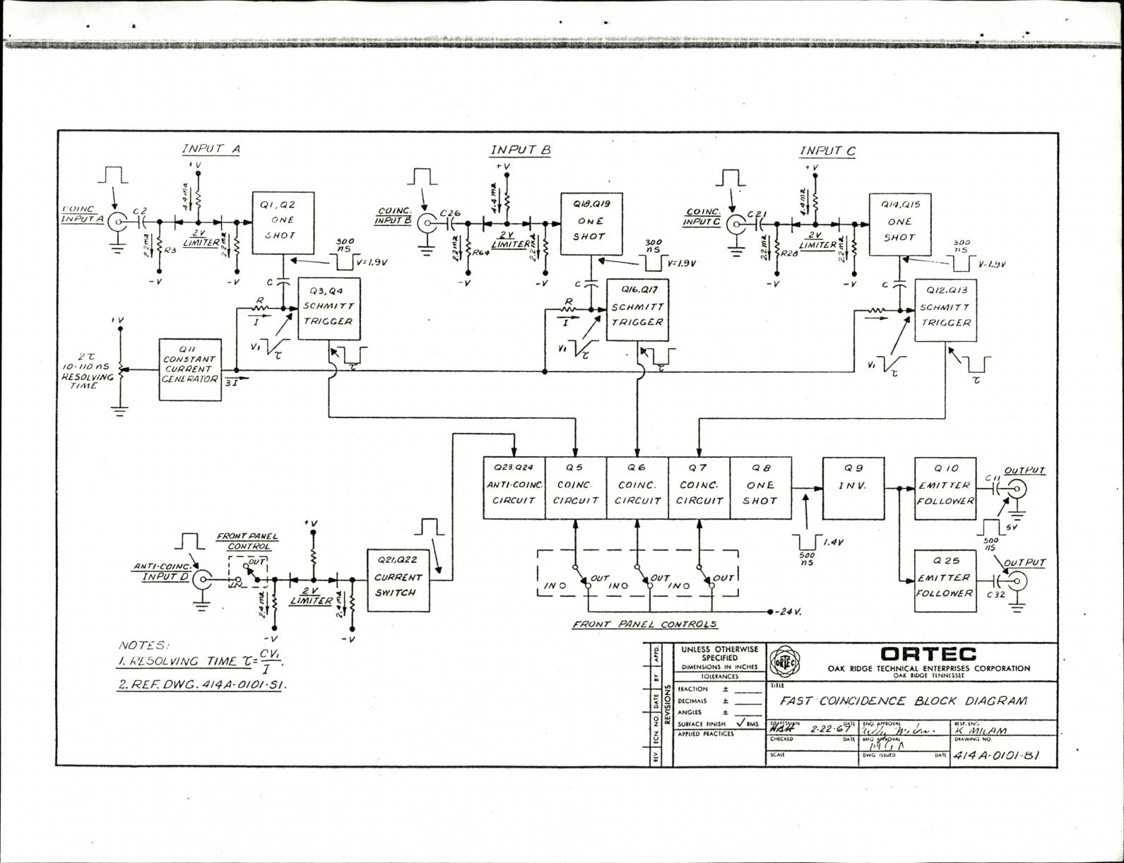
5.
CIRCUIT
DESCRIPTION
(Etched
Board
220
-
164)
The
fast
coincidence
circuit
consists
of
three
identical
coincidence
input
stages
and
an
anticoincidence
input
stage,
all
feeding
in
parallel
to
a
coincidence
stage
or
AND
gate
(see
Drawings
414A-0164-S1
and
414A-0101-B1).
The
coincidence
stage
is
composed
of
transistors
Q5,
Q6,
Q7,
and
Q24,
which
constitute
one
side
of
a
one-shot
trigger
circuit,
and
Q8,
which
constitutes
the
other
side.
The
output
of
this
trigger
circuit
is
fed
to
Q9,
where
it
is
inverted
and
sent
to
QlO
and
Q25,
the
output
emitter-followers.
The
coincidence
input
signals
are
all
regenerated
in
the
regeneration
and
pulse
forming
stages;
for
example,
coincidence
Input
A
signal
is
regenerated
by
the
one-shot
trigger
circuit
Q1
and
02
and
is
again
reshaped
and
fed
out
by
the
ac-coupled
Schmitt
trigger
circuit
03
and
04
to
05,
The
input
signal
is
fed
into
regeneration
circuit
01
and
02
through
a
2-V
limiter
consisting
of
resistors
R2,
R3,
R5,
and
R8.
The
limiting
action
is-accomplished
by
switching
the
constant
current
that
normally
flows
through
D2
and
R3
through
limiter
load
resistor
R5
by
the
application
of
a
positive
input
signal
on
Input
A.
The
2t
resolving
time
is
set
by
the
On
duration
of
the
ac-coupled
Schmitt
trigger
circuit
03
and
04.
The
signal
input
to
03
is
a
negative-going
pulse
with
a
precisely
controlled
amplitude
from
the
collector
of
01.
The
negative-going
pulse
is
coupled
through
C4
to
the
base
of
03
and
turns
off
03.
03
remains
off
for
a
duration
t.
The
constant-current
generator
Oil
and
series
resistor
R12
control
the
duration,
t,
by
discharging
capacitor
C4
back
from
its
negative
value
toward
ground.
When
the
voltage
at
03
exceeds
ground
potential,
03
again
is
switched
on
and
04
is
turned
off.
The
duration
that
04
remains
on
constitutes
one-half
the
resolving
time,
i.e.,
t.
The
output
of
04
is
a
negative-going
pulse
which
turns
off
05
in
the
coincidence
circuit
and
combination
one-shot
multivibrator.
The
anticoincidence
input
has
a
similar
voltage
limiter,
a
current
switch
(021
and
022),
and
a
voltage
clamp
which
turns
024
on
or
off.
The
anticoincidence
circuit
is
dc-coupled
from
the
input
to
024;
therefore
024
may
be
turned
on
by
a
pulse
or
a
dc
voltage.
The
combination
of
05, 06,
07,
and
024
constitutes
one
side
of
a
one-shot
trigger
circuit,
with
08
constituting
the
other
side.
024,
the
anticoincidence
input,
is
normally
biased
off,
while
05, 06,
and
07,
the
coincidence
inputs,
are
normally
biased
on.
In
the
event
that
05,
06,
and
07
are
all
turned
off
simultaneously
and
024
is
not
turned
on
by
an
anticoincidence
input,
the
one-shot
multivibrator
circuit
is
triggered,
and
08
conducts
the
normal
current
flowing
through
R26.
A
negative-going
pulse
is
formed
at
the
collector
of
08
and
is
inverted
by
09.
The
output
signal
of
invertor
09
is
fed
through
emitter-followers
.010
and
024,
and
thence
to
the
output
BNC
connectors.
The
constant-current
generator
Oil
generates
a
current
which
is
equal
to
31.
This
current
is
then
split
into
three
equal
parts,
with
one
part
going
to
each
of
the
three
input
pulse-forming
circuits,
i.e.,
03-04,
017-016,
and
012-013.
Either
A,
B,
or
C
front
panel
control
switch
(SI,
S2,
or
S3)
can
disable
one
coincidence
input
of
the
combination
threefold
coincidence
and
one-shot
multivibrator
circuit
composed
of
05,
,06,
07,
024,
and
08
(see
Drawing
414A-0101-S1).
When
one
of
these
switches
is
moved
to
Out,
the
transistor
corresponding
to
that
switch
is
reverse-biased,
resulting
in
a
twofold
coincidence
circuit.
The
actual
coincidence
recognition
is
performed
by
transistors
05,
06,
and
08,
while
024
acts
to
inhibit
the
coincidence
output
when
a
signal
is
applied
to
the
anticoincidence
input.
The
anticoincidence
input
can
be
disabled
by
placing
switch
D
(S4)
to
the
Out
position.
This
interrupts
the
signal
to
the
anticoincidence
circuit.
With
front
panel
control
switches
A,
B,
and
C
all
placed
to
In,
a
current
of
approximately
3
mA
flows
through
R26
and
then
is
passed
through
transistors
05,
06,
and
07
in
parallel
and
thence
through
R23.
Moving
switch
A,
B,
or
C
to
Out
back-biases
the
particular
transistor
associated
with
that
switch,
thus
making
the
series
path
consist
of
R26,
the
two
remaining
transistors,
and
R23.
With
the
application
of
simultaneous
negative
input
pulses
to
05,
06,
and
07
and
in
the
absence
of
an
anticoincidence
pulse
to
turn
on
024,
the
current
flow
through
R23
ceases
and
a
positive
pulse
is
coupled
through
CIO
into
the
base
of
08.
08
conducts
for
a
time
constant
determined
by
CIO
and
R24,
thereby
back-biasing
the
parallel
combination
of
05,
06,
and
07.
Notice
that
in
the
quiescent
state
08
is
back-biased
by
the
voltage
drop
across
diode
D9,
since
09
is
forward-biased
with
a
current
of
1
mA.
6.
MAINTENANCE
I
ai.
TESTING
PERFORMANCE
The
following
paragraphs
are
Intended
as
aids
in
the
installation
and
checkout
of
the
414A.
These
instructions
present
information
on
front
panel
controls,
waveforms,
at
test
points,
and
output
connectors.
The
following,
or
equivalent,
test
equipment
is
needed:
ORTEC
419
Precision
Pulse
Generator
Tektronix
Model
580
Oscilloscope
100S2
BNC
terminators
Vacuum
tube
voltmeter
ORTEC
410
Linear
Amplifier
Two
ORTEC
420A
Timing
Single
Channel
Analyzers
Schematic
and
block
diagram
for
414A
Preliminary
procedures
consist
of
the
following:
1.
Visually
check
module
for
possible
damage
due
to
shipment.
2.
Connect
ac
power
to
ORTEC
401
/402.
3.
Plug
module
into
Bin
and
check
for
proper
mechanical
alignment.
4.
Switch
on
ac
power
and
check
the
dc
Power
Supply
voltages
at
the
test
points
on
the
402
control
panel.
Testing
the
performance
of
the
414A
involves
the
following:
1.
Feed
the
output
of
the
420A
into
coincidence
Input
A.
Terminate
with
lOOfi
the
RG-62/U
connecting
cable
feeding
Input
A.
2.
Set
the
In/Out
control
toggle
switches
as
follows:
A,
In;
B,
C,
and
D,
Out.
3.
Set
the
Resolving
Time
control
to
100.
4.
Observe
the
Fast
Coincidence
output
pulse;
it
should
be
a
positive
pulse,
6.5
±
0.6
V
and
0.5
±
0.1
/isec
wide.
Loading
the
414A
Output
with
100J2
should
reduce
the
output
to
not
less
than
5
V
and
the
width
to
not
less
than
0.5psec.
5.
Putting
In/Out
switch
B
or
C
to
the
In
position
should
inhibit
the
pulse
on
the
414A
Output.
Check
that
both
B
and
C
inhibit.
Connect
the
input
into
Input
8
and
check
that
both
A
and
C
inhibit.
Connect
the
input
into
Input
C
and
check
that
both
A
and
B
inhibit.
6.
Connect
the
equipment
as
shown
in
Fig.
6.1;
Keep
all
coaxial
cables
terminated
in
their
characteristic
impedance.
7.
Ensure
that
a
positive
logic
pulse
is
being
received
from
the
output
of
each
420A.
Set
the
output
delay
control
on
the
Calibrated
420A
to
200
and
adjust
the
Reference
420A
output
pulse
until
the
leading
edges
of
the
pulses
are
approximately
in
coincidence.
414A
FAST
COINCIDENCE
RESOLVING
TIME
Refer
enc«
Out
out
outout
Calibrated
300673
PRECISION
PULSE
GENERATOR
419
LINEAR
AMPLIFIER
410
TIMING
SINGLE
CHANNEL
ANALYZER
420A
TIMING
SINGLE
CHANNEL
ANALYZER
420A
Channel
Exterior
1
Trigger
OSCILLOSCOPE
Fig.
6.1.
414A
Test
and
Calibrate
Circuit.
8.
Set
the
In/Out
Control
switches
as
follows:
A
and
B,
In;
C
and
D,
Out.
9.
Set
the
Resolving
Time
control
to
1
TOO.
10..
With
the
equipment
connected
as
shown
in
Fig.
6.1,
two
pulses
(the
Calibrated
420A
output
and
the
414A
output)
should
be
visible
on
the
oscilloscope.
Set
the
horizontal
time
base
to
20
nsec/cm.
It
may
be
necessary
to
use
the
Delayed
Sweep
function
on
the
oscilloscope
in
order
to
observe
both
pulses
at
this
horizontal
sweep
speed.
11.
Decrease
the
output
delay
control
on
the
Calibrated
420A
until
the
414A
output
pulse
disappears.
12.
Increase
the
output
delay
control
on
the
Calibrated
420A,
and
the
414A
output
pulse
should
reappear
and
disappear
again
as
the
delay
is
increased.
Measure
the
change
in
delay
of
the
Calibrated
420A
pulse
from
the
time
that
the
414A
output
pulse
reappears
until
it
disappears
again.
This
time
can
be
accurately
measured
looking
at
the
oscilloscope.
The
time
measured
represents
the
2t
resolving
time
of
the
414A
with
the
Resolving
Time
control
set
at
1100
and
should
be
110-150
nsec.
13.
Connect
the
Calibrated
420A
output
to
Input
C
on
the
414A.
14.
Set
the
In/Out
control
switches
as
follows:
A
and
C,
In;
B
and
D,
Out.
15.
Repeat
steps
.9
through
12.
16.
Connect
the
Reference
420A
output
to
Input
B
on
the
414A.
17.
Set
the
In/Out
control
switches
as
follows:
A
and
D,
Out;
B
and
C,
In.
18.
Repeat
steps
9
through
12.
19.
Repeat
steps
9
through
16
with
the
following
exceptions:
a.
In
step
9
set
the
Resolving
Time
control
to
100.
b.
In
step
10
set
the
oscilloscope
horizontal
time
base
to
10
nsec/cm.
c.
In
step
12
the
2t
resolving
time
should
be
less
than
10
nsec
with
the
Resolving
Time
control
set
at
100.
20.
Set
the
output
delay
control
on
the
Calibrated
420A
so
that
its
output
occurs
approximately
100
nsec
prior
to
the
Reference
420A
output.
21.
Connect
the
Reference
420A
output
to
the
414A
Input
A.
22.
Connect
the
Calibrated
420A
output
to
the
414A
Input
D.
23.
Set
the
Resolving
Time
control
to
1100.
24.
Set
the
In/Out
control
switches
as
follows:
A,
In;
B,
C,
and
D,
Out.
25.
A
pulse
should
be
present
at
the
output
of
the
414A.
Place
In/Out
control
switch
D
to
the
In
position,
and
the
414A
output
pulse
should
disappear.
6.2.
ALIGNMENT
OF
RESOLVING
TIME
TRIMMER
CAPACITORS
If
the
resolving
time
readings
(Section
6.1)
were
not
satisfactory,
the
trimmer
capacitors
in
each
resolving
network
may
be
adjusted
to
optimize
the
resolving
time
in
each
channel:
1.
,
Connect
and
adjust
the
equipment
as
stated
in
Section
6.1,
steps
6
and
7.
2.
Set
the
In/Out
control
switches
as
follows:
A,
In;
B,
C,
and
D,
Out.
3.
Set
the
Resolving
Time
control
to
100.
4.
Observe
the
414A
output
with
an
oscilloscope.
5.
Using
an
insulated
screwdriver,
adjust
capacitor
C4
until
the
output
pulse
disappears.
Continue
to
rotate
C4
adjustment
until
the
output
reappears.
Stop
the
adjustment
of
C4
as
soon
as
an
output
pulse
appears
for
each
input
pulse.
6.
Set
the
In/Out
control
switches
as
follows:
A,
C,
and
D,
Out;
B,
In.
7.
Adjust
C23
as
explained
in
step
5.
8.
Connect
Reference
420A
to
Input
C.
9.
Set
the
In/Out
control
switches
as
follows:
A,
B,
and
D,
Out;
C,
In.
10.
Adjust
C18
as
explained
in
step
5.
11.
Perform
the
tests
outlined
in
Section
6.1,
steps
1
—
25,
to
check
the
instrument
performance.
6.3.
SUGGESTIONS
FOR
TROUBLESHOOTING
In
situations
where
the
414A
is
suspected
of
malfunction,
it
is
essential
to
verify
such
malfunction
in
terms
of
simple
pulse
generator
impulses
at
the
input
and
output.
The
414A
must
be
disconnected
from
its
position
in
any
system,
and
routine
diagnostic
analysis
performed
with
a
test
pulse
generator
and
oscilloscope.
It
is
imperative
that
testing
not
be
performed
with
a
source
and
detector
until
the
amplifier
and
logic
inputs
to
the
Fast
Coincidence
unit
perform
satisfactorily
with
the
test
pulse
generator.
The
testing
instructions
in
Section
6.1
of
this
manual
and
the
circuit
description
in
Section
5
should
provide
assistance
in
locating
the
region
of
trouble
and
in
repairing
the
malfunction.
The
guide
plate
and
shield
cover
can
be
completely
removed
from
the
module
to
enable
oscilloscope
and
voltmeter
observations
with
a
minimal
chance
of
accidentally
short-circuiting
portions
of
the
etched
board.
The
414A
may
be
returned
to
ORTEC
for
repair
service
at
nominal
cost.
Our
standardized
procedure
requires
that
each
repaired
instrument
receive
the
same
extensive
quality
control
tests
that
a
new
instrument
receives.
Contact
our
Customer
Service
Department,
(615)
4824411,
for
shipping
instructions
before
returning
the
instrument.
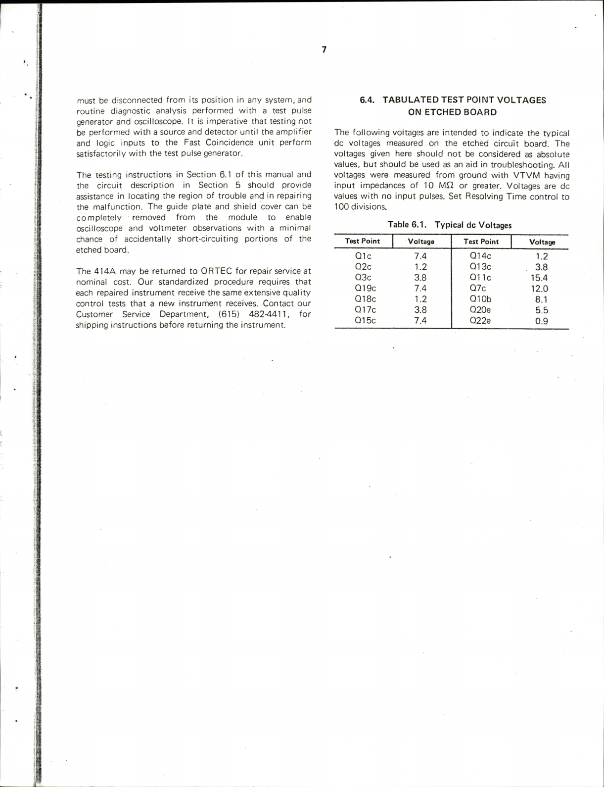
6.4.
TABULATED
TEST
POINT
VOLTAGES
ON
ETCHED
BOARD
The
following
voltages
are
intended
to
indicate
the
typical
dc
voltages
measured
on
the
etched
circuit
board.
The
voltages
given
here
should
not
be
considered
as
absolute
values,
but
should
be
used
as
an
aid
in
troubleshooting.
All
voltages
were
measured
from
ground
with
VTVM
having
input
impedances
of
10
or
greater.
Voltages
are
dc
values
with
no
input
pulses.
Set
Resolving
Time
control
to
100
divisions.
Table
6.1.
Typical
dc
Voltages
Test
Point
Voltage
Test
Point
Voltage
QIC
7.4
Ql4c
1.2
Q2c
1.2
013c
3.8
Q3c
3.8
011c
15.4
019c
7.4
07c
12.0
QiSc
1.2
010b
8.1
Ql7c
3.8
O20e
5.5
Ql5c
7.4
022e
0.9

BIN/MODULE
CONNECTOR
PIN
ASSIGNMENTS
FOR
AEC
STANDARD
NUCLEAR
INSTRUMENT
MODULES
PER
TID-20893
Pin
Function
Pin
Function
1
+3
volts
23
Reserved
2
—3
volts
24
Reserved
3
Spare
Bus
25
Reserved
4
Reserved
Bus
26
Spare
5
Coaxial
27
Spare
6
Coaxial
*28
+24
volts
■
7
Coaxial
*29
—24
volts
8
200
volts
dc
30
Spare
Bus
9
Spare
31
Spare
*10
+6
volts
32
Spare
*11
—6
volts
*33
115
volts
ac
(Hot)
12
Reserved
Bus
*34
Power
Return
Ground
13
Spare
**35
Reset
(Sealer)
14
Spare
**36
Gate
15
Reserved
**37
Reset
(Auxiliary)
*16
+
12
volts
38
Coaxial
*17
—12
volts
39
Coaxial
18
Spare
Bus
40
Coaxial
19
Reserved
Bus
*41
115
volts
ac
(Neut.)
20
Spare
*42
High
Quality
Ground
21
Spare
G
Ground
Guide
Pin
22
Reserved
Pins
marked
(*)
are
Installed
and
wired
in
ORTEC
401A
and
401B
Modular
System
Bins.
Pins
marked
(*)
and
(**)
are
installed
and
wired
in
EG&G/ORTEC—HEP
M250/N
and
M350/N
NIMBINS.
iBIiiWtM'aiWIMCiiWI
INPU
T
INPUT
B
INPUTC
QiS.QI9
Qf^.QlS
ONL
'J
HOT
Qt
.az
(
UtNC
COlhJC
OINC.
jMPur
A
INPUT
OnL
INPUT
C
r'<\
2}L
^
iiMiriR^
6Hor
UAl/TSR
Q/e>.Q/7
Qiz.aii
schnutt
TRICCER
SCHMtTT
TRICCER
SCHM/TT
QU
constant
CURRENT
CLNIPATOR
ZX
lO-no
ns
RE50LV/NC
T/Al€
FRONT
PANEL
CONTROL
QZLQ2Z
ANTt-COtNC
2
INPUT
D
swtrcN
LimiTER
023.024
AUT/COIUC.
CIPCUIT
QS
COITIC
CIPCUl
T
a
e
COINC.
CIRCUIT
Q7
COINC.
CIRCUIT
aa
ONE
SHOT
IN
O
Q
10
£Ml
T
TCP
FOLLOTIER
Output
r\j'
500
n5
500
rl5
INO
ipur
V
^NO
a
25
EAMTTE-R
follower
\
OUTPUT
C'SZ
9-24)/.
rPONT
P/^N£L
CONTROLS
AOT£S:
C\/,
/.
A'£50L
VINC
TIML
Z-
2.
RLE
DWG.
4l4A-OIOI-5t.
-V
UNLESS
OTHERWISE
SPECIFIED
Dimensions
in
inches
E8AC1ION
i
DECiMAlS
±
ANCIES
SUIEaCE
EINISH
v^li
APriiEO
MACIlCES
ORTEC
OAK
RIDGE
TECHNICAL
ENTERPRISES
CORPORATION
OAK
liDOE
UNNtSSEE
FAST
COJNCiDBNCE
SLOCK
DIACPAM
2-22C.r
tNy
^WIOVM
!
m
lA.
OtvG
i^WiO
itir
{NO
K
MIlAM
PIAWINU
NO.
4l4A-0l0l-(il
-CZ5I1-
—Igcaf—
•H
oSah-
/'jo
H
goiat-
-
•+
oe-3
—
e£D
+
—
H
8tah-
—I
sz
^
I—
—I
—
ngj—
—I
O
<Q
—
+
-qtd—
-da)
•90+
—
-{WttJ—
-CE3J-
•
I—
r
-|£zah-
—l"Z-t.ah-
CSS)
—1
Slat—
-fgrST—rTT>-
S
h
—C~±£2_I)—
--(goTdj--
H
^aK
-[WS}-
—i
oil2<
h~
H
e=ja
-j
so-<-|—
Hy^al
<H
920I—
—{^cFdT—
—C
3
)—
^
j
—I
"fri
a
h-
lHU
—rrrsj>-
-mTu=
—(
/ga>—
—I
naH-f
$
—1
csa
I—
-<
9a
K-
-czzi—
h-
-C
9za
>-
-moT^
jj-jsor^^
-*4TTO|—
—<~0Id
'y—
-CHS—
—
xx^C^sZH™
~-S52}-~
-Q51}—
•^£5353""
"*Hozo
I—
eco4.--
Table of contents
Other EG&G Amplifier manuals

EG&G
EG&G ORTEC 444 User manual

EG&G
EG&G 128A Service manual

EG&G
EG&G ORTEC 575A Service manual

EG&G
EG&G ORTEC 118A User manual

EG&G
EG&G ORTEC 474 Service manual

EG&G
EG&G ORTEC 535 Service manual

EG&G
EG&G ORTEC 427 User manual

EG&G
EG&G 113 Service manual

EG&G
EG&G ORTEC 113 Service manual

EG&G
EG&G ORTEC 855 Service manual


