EG&G ORTEC 575A Service manual

n
!
Mode!
575A
Ampl
ifier
Operating
and
Service
Manual
>—1
T.
fe
•fl

Printed
in
U.S.A.
Model
575A
Ampl
ifier
Operating
and
Service
Manual
This
manual
applies
to
instruments
marked
"Rev
03"
on
rear
panel
EG&G
ORTEC
Part
Number
717460
3152
1
.OC
0189

ill
CONTENTS
Page
WARRANTY
\
PHOTOGRAPHS
VI
1.
DESCRIPTION
1
1.1.
General
1
1.2.
Pole-Zero
Cancellation
1
1.3.
Active
Filter
3
2.
SPECIFICATIONS
4
2.1.
Performance
4
2.2.
Controls
4
2.3.
Input
! ! !
.
4
2.4.
Outputs
4
2.5.
Related
Equipment
4
2.6.
Electrical
and
Mechanical
4
3.
INSTALLATION
5
3.1.
General
'
5
3.2.
Connection
to
Power
5
3.3.
Connection
to
Preamplifier
5
3.4.
Connection
of
Test
Pulse
Generator
5
3.5.
Shaping
Considerations
5
3.6.
Linear
Output
Connections
and
Terminating
Considerations
6
3.7.
Shorting
or
Overloading
the
Amplifier
Output
6
4.
OPERATION
7
4.1.
Initial
Testing
and
Observation
of
Pulse
Waveforms
7
4.2.
Front
Panel
Controls
7
4.3.
Panel
Connectors
7
4.4.
Standard
Setup
Procedure
8
4.5.
Pole-Zero
Adjustment
8
4.6.
Operation
with
Semiconductor
Detectors
9
4.7.
Operation
in
Spectroscopy
Systems
11
4.8.
Other
Experiments
13
5.
CIRCUIT
DESCRIPTION
15
6.
MAINTENANCE
16
6.1.
Test
Equipment
Required
16
6.2.
Pulser
Test
16
6.3.
Suggestions
for
Troubleshooting
17
6.4.
Factory
Repair
17
6.5.
Tabulated
Test
Point
Voltages
17
Schematic
700000

Iv
ILLUSTRATIONS
Page
Fig.
1.1.
Differentiation
in
an
Amplifier
Without
Pole-Zero
Cancellation
2
Fig.
1.2.
Differentiation
in
a
Pole-Zero
Cancelled
Amplifier
2
Fig.
1.3.
Pulse
Shapes
for
Good
Signal-to-Noise
Ratios
3
Fig.
4.1.
Typical
Unipolar
and
Bipolar
Output
Waveforms
'
Fig.
4.2.
Settings
for
Time-Constant
Jumpers
'
Fig.
4.3.
Typical
Waveforms
Illustrating
Pole-Zero
Adjustment
Effects
°
Fig.
4.4.
A
Clamp
Circuit
that
can
be
used
to
Prevent
Overloading
the
Oscilloscope
9
Fig.
4.5.
Pole-Zero
Adjustment
Using
a
Square
Wave
Input
to
the
Preamplifier
9
Fig.
4.6.
System
for
Measuring
Amplifier
and
Detector
Noise
Resolution
10
Fig.
4.7.
Noise
as
a
Function
of
Bias
Voltage
Fig.
4.8.
System
for
Measuring
Resolution
with
a
Pulse
Height
Analyzer
11
Fig.
4.9.
System
for
Detector
Current
and
Voltage
Measurements
11
Fig.
4.10.
Silicon
Detector
Back
Current
vs
Bias
Voltage
11
Fig.
4.11.
System
for
High-Resolution
Alpha-Particle
Spectroscopy
12
Fig.
4.12.
System
for
High-Resolution
Gamma
Spectroscopy
12
Fig.
4.13.
Scintillation-Counter
Gamma
Spectroscopy
System
12
Fig.
4.14.
High-Resolution
X-Ray
Energy
Analysis
System
Using
a
Proportional
Counter
13
Fig.
4.15.
Gamma-Ray
Charged-Particle
Coincidence
Experiment
13
Fig.
4.16.
Gamma-Ray
Pair
Spectrometry
Fig.
4.17.
Gamma-Gamma
Coincidence
Experiment
l^
Fig.
5.1.
Amplifier
Block
Diagram
Fig.
6.1.
Circuit
Used
to
Measure
Nonlinearity
16

standard
Warranty
for
EG&G
ORTEC
Nuclear
Electronic
Instruments
EG&G
ORTEC
warrants
that
the
items
will
be
delivered
free
from
defects
in
material
or
workmanship.
EG&G
ORTEC
makes
no
other
warranties,
express
or
implied,
and
specifically
NO
WARRANTY
OF
MERCHANTABILITY
OR
FITNESS
FOR
A
PARTICULAR
PURPOSE.
EG&G
ORTEO's
exclusive
liability
is
limited
to
repairing
or
replacing
at
EG&G
ORTEO's
option,
items
found
by
EG&G
ORTEC
to
be
defective
in
workmanship
or
materials
within
two
years
from
the
date
of
delivery,
EG&G
ORTEO's
liability
on
any
claim
of
any
kind,
including
negligence,
loss
or
damages
arising
out
of,
connected
with,
or
from
the
performance
or
breach
thereof,
or
from
the
manufacture,
sale,
delivery,
resale,
repair,
or
use
of
any
item
or
services
covered
by
this
agree
ment
or
purchase
order,
shall
in
no
case
exceed
the
price
allocable
to
the
item
or
service
furnished
or
any
part
thereof
that
gives
rise
to
the
claim.
In
the
event
EG&G
ORTEC
fails
to
manufacture
or
deliver
items
called
for
in
this
agreement
or
pur
chase
order,
EG&G
ORTEO's
exclusive
liability
and
buyer's
exclusive
remedy
shall
be
release
of
the
buyer
from
the
obliga
tion
to
pay
the
purchase
price.
In
no
event
shall
EG&G
ORTEC
be
liable
for
special
or
consequential
damages.
Quality
Control
Before
being
approved
for
shipment,
each
EG&G
ORTEC
nuclear
electronic
instrument
must
pass
a
stringent
set
of
quality
control
tests
designed
to
expose
any
flaws
in
materials
or
workmanship.
Permanent
records
of
these
tests
are
maintained
for
use
in
warrany
repair
and
as
a
source
of
statistical
information
for
design
improvements.
Repair
Service
If
it
becomes
necessary
to
return
this
instrument
for
repair,
it
is
essential
that
Customer
Services
be
contacted
in
advance
of
its
return
so
that
a
Return
Authorization
Number
can
be
assigned
to
the
unit.
Also,
EG&G
ORTEC
must
be
informed,
either
in
writing,
by
telephone
[(615)
482-4411]
or
by
telex
(55-7450)
of
the
nature
of
the
fault
of
the
instrument
being
re
turned
and
of
the
model,
serial,
and
revision
("Rev"
on
rear
panel)
numbers.
Failure
to
do
so
may
cause
unnecessary
delays
in
getting
the
unit
repaired.
The
EG&G
ORTEC
standard
procedure
requires
that
instruments
returned
for
repair
pass
the
same
quality
control
tests
that
are
used
for
new-production
instruments.
Instruments
that
are
returned
should
be
packed
so
that
they
will
withstand
normal
transit
handling
and
must
be
shipped
PREPAID
via
Air
Parcel
Post
or
United
Parcel
Service
to
the
nearest
EG&G
ORTEC
repair
center.
(In
the
case
where
the
instrument
did
not
function
upon
pur
chase,
EG&G
ORTEC
will
pay
shipment
costs
both
ways.)
The
address
label
and
the
package
should
include
the
Return
Authorization
Number
assigned.
Instruments
being
returned
that
are
damaged
in
transit
due
to
inadequate
packing
will
be
repaired
at
the
sender's
expense,
and
it
will
be
the
sender's
responsibility
to
make
claim
with
the
shipper.
Instruments
not
in
warranty
will
be
repaired
at
the
standard
charge
unless
they
have
been
grossly
misused
or
mishandled,
in
which
case
the
user
will
be
notified
prior
to
the
repair
being
done.
A
quotation
will
be
sent
with
the
notification.
Damage
in
Transit
Shipments
should
be
examined
immediately
upon
receipt
for
evidence
of
external
or
concealed
damage.
The
carrier
making
delivery
should
be
notified
immediately
of
any
such
damage,
since
the
carrier
is
normally
liable
for
damage
in
shipment.
Packing
materials,
waybills,
and
other
such
documentation
should
be
preserved
in
order
to
establish
claims.
After
such
notification
to
the
carrier,
please
notify
EG&G
ORTEC
of
the
circumstances
so
that
assistance
can
be
provided
in
making
damage
claims
and
in
providing
replacement
equipment
if
necessary.

i

EG&G
ORTEC
MODEL
575A
AMPLIFIER
1.
DESCRIPTION
1.1.
GENERAL
The
EG&G
ORTEC
575A
Amplifier
is
a
single-width
NIM
module
that
features
a
versatile
combination
of
jumper-
selectable
pulse-shaping
characteristics.
The
amplifier
has
extremely
low
noise,
a
wide
gain
range,
and
excellent
overload
response
for
universal
application
in
high-
resolution
spectroscopy.
It
accepts
input
pulses
of
either
polarity.
Input
may
originate
from
germanium
or
silicon
semiconductor
detectors,
from
scintillation
counters
with
either
fast
or
slow
scintillators,
from
proportional
count
ers,
from
pulsed
ionization
chambers,
from
electron
multipliers,
etc.
The
unit
has
an
input
impedance
of
~1000
O
and
accepts
either
positive
or
negative
input
pulses
with
rise
times
<650
ns
and
fall
times
>30
/js.
Three
integration
and
differentiation
time
constants
are
jumper-selectable
on
the
printed
wiring
board
(PWB)
to
provide
optimum
shap
ing
for
resolution
and
count
rate.
The
differentiation
net
work
has
variable
pole-zero
cancellation
that
can
be
adjusted
to
match
preamplifiers
with
decay
times
>30
/js.
The
pole-zero
cancellation
drastically
reduces
the
under
shoot
after
the
differentiator
and
greatly
improves
over
load
and
count
rate
characteristics.
In
addition,
the
amplifier
contains
an
active,
filter-shaping
network
that
optimizes
the
signal-to-noise
ratio
and
minimizes
the
overall
resolving
time.
The
amplifier
has
unipolar
and
bipolar
BNC
outputs.
The
unipolar
output
is
used
for
spectroscopy
in
systems
where
dc
coupling
can
be
maintained
from
the
575A
to
the
analyzer.
A
BLR
(baseline
restorer)
circuit
is
included
in
the
unit
for
improved
performance
at
all
count
rates.
Baseline
correction
is
applied
only
during
intervals
be
tween
input
pulses
and
automatically
selects
a
discrimi
nator
level
to
identify
input
pulses.
The
unipolar
output
dc
level
is
within
the
range
of
-5
mV
to
+5
mV.
This
output
permits
the
use
of
the
direct-coupled
input
of
the
analyzer
with
a
minimum
amount
of
interface
problems.
The
575A
can
be
used
for
constant-fraction
timing
when
operated
in
conjunction
with
an
EG&G
ORTEC
551, 552,
or
553
Timing
Single-Channel
Analyzer.
The
EG&G
ORTEC
Timing
Single-Channel
Analyzers
feature
a
mini
mum
of
walk
as
a
function
of
pulse
amplitude
and
incor
porate
a
variable
delay
time
on
the
output
pulse
to
enable
the
timing
pickoff
output
to
be
placed
in
time
coincidence
with
other
signals.
The
575A
has
complete
provisions,
including
power
dis
tribution,
for
operating
any
EG&G
ORTEC
solid-state
preamplifier.
Normally,
the
preamplifier
pulses
should
have
a
rise
time
of
0.25
/js
or
less
to
properly
match
the
amplifier
filter
network
and
a
decay
time
>30/us
for
proper
pole-zero
cancellation.
The
input
impedance
is
1000
Q.
When
long
preamplifier
cables
are
used,
the
cables
can
be
terminated
in
series
at
the
preamplifier
end
or
in
shunt
at
the
amplifier
end
with
the
proper
resistors.
The
output
impedance
is
—0.2
Q,
and
the
output
can
be
connected
to
other
equipment
by
a
single
cable
going
to
all
equipment.
The
cable
must
be
shunt-terminated
at
the
far
end.
(See
Section
3
for
further
information.)
1.2.
POLE-ZERO
CANCELLATION
Pole-zero
cancellation
is
a
method
for
eliminating
pulse
undershoot
after
the
differentiating
network.
In
an
am
plifier
not
using
pole-zero
cancellation
(Fig.
1.1)
the
ex
ponential
tail
on
the
preamplifier
output
signal
(usually
50
to
500/ys)
causes
an
undershoot
whose
peak
amplitude
is
roughly
determined
from;
undershoot
amplitude
differentiated
pulse
amplitude
_
differentiation
time
preamplifier
pulse
decay
time.
'
For
a
1-/7S
differentiation
time
and
a
50-/js
pulse
decay
time
the
maximum
undershoot
is
2%,
and
this
decays
with
a
50-/JS
time
constant.
Under
overload
conditions
this
undershoot
is
often
sufficiently
large
to
saturate
the
am
plifier
during
a
considerable
portion
of
the
undershoot,
causing
excessive
dead
time.
This
effect
can
be
reduced
by
increasing
the
preamplifier
pulse
decay
time
(which
generally
reduces
the
counting
rate
capabilities
of
the
preamplifier)
or
compensating
for
the
undershoot
by
providing
pole-zero
cancellation.
Pole-zero
cancellation
is
accomplished
by
the
network
shown
in
Fig.
1.2.
The
pole
[s
+
(1/To)]
due
to
the
pream
plifier
pulse
decay
time
is
cancelled
by
the
zero
of
the
network
[s
+
(k/R2Ci)].
In
effect,
the
dc
path
across
the
differentiation
capacitor
adds
an
attenuated
replica
of
the
preamplifier
pulse
to
just
cancel the
negative
undershoot
'
of
the
differentiating
network.
Total
preamplifier-amplifier
pole-zero
cancellation
re
quires
that
the
preamplifier
output
pulse
decay
time
be
a
single
exponential
decay
and
be
matched
to
the
pole-
zero
cancellation
network.
The
variable
pole-zero
cancel
lation
network
allows
accurate
cancellation
for
all
pream
plifiers
having
30-/js
or
greater
decay
times.
Improper
matching
of
the
pole-zero
network
will
degrade
the
over
load
performance
and
cause
excessive
pileup
distortion
at
medium
counting
rates.
Improper
matching
causes
either
an
undercompensation
(undershoot
is
not
elimi
nated)
or
an
overcompensation
(output
after
the
main
pulse
does
not
return
to
the
baseline
but
decays
to
the
baseline
with
the
preamplifier
time
constant).
The
pole-

eo(t)
.
(t)
Undershoot
.
cir«t
Differentiated
outpS
'"'*
X
differentiate
=
network
rirshoot
1
s
X
:
=
Ei(s)
(Laplace
transform).
■max
1
s
+
-^
s
+
„
-
To
R|Ci
200409
To
-
r,
■To
e-^^To
_
T",
g-t/To
=e,
where
F,
=
RiC,
.
Fig.
1.1.
Differentiation
in
an
Amplifier
Without
Pole-Zero
Cancellation.
0
</<■<!
®oW
=
fmax
"
No
Undershoot
Pole-zero
Differentiated
Charge
loop
y
cancelled
,
pulse
output
^
differentiate
without
network
undershoot
Pole
zero
cancel
by
letting
1
K
s
+
—
=
s
+
■
To
RjCi
fmax
■
1
^
^
R
C
^max
T"
*
'
,
'p
=
fi
(iF
(Laplace
transform).
1
KI
+
n2
S+
—
5+-
To
R1
R:
Ci
200410
S
+
cmax cmax
_
^
,
„
R,
R,
"5—TH—
1
-
11
(s),
where
Rn
=
„
„
Ri
+R2
J
^
Ri
+
R2
R1
R2
Cj
RpCj
Fig.
1.2.
Differentiation
in
a
Pole-Zero
Cancelled
Amplifier.

zero
adjust
is
accessible
on
the
front
panel
of
the
575A
and
can
easily
be
adjusted
by
observing
the
baseline
on
an
oscilloscope
with
a
monoenergetic
source
or
pulser
having
the
same
decay
time
as
the
preamplifier
under
overload
conditions.
The
adjustment
should
be
made
so
that
the
pulse
returns
to
the
baseline
in
the
minimum
time
with
no
undershoot.
1.3.
ACTIVE
FILTER
When
only
FET
gate
current
and
drain
thermal
noise
are
considered,
the
best
signal-to-noise
ratio
occurs
when
the
two
noise
contributions
are
equal
for
a
given
input
pulse
shape.
The
gaussian
pulse
shape
(Fig.
1.3)
for
this
condition
requires
an
amplifier
with
a
single
RC
differen
tiation
and
n
equal
RC
integrations
where
n
approaches
infinity.
The
Laplace
transform
of
this
transfer
function
is
G(s)
1
s-F(1/RG)
[s+(1/RC)]"
(n
-
0C),
where
the
first
factor
is
the
single
differentiation,
and
the
second
factor
is
the
n
integrations.
The
active
filter
ap
proximates
this
transfer
function.
Figure
1.3
illustrates
the
results
of
pulse
shaping
in
an
amplifier.
Of
the
four
pulse
shapes
shown
the
cusp
would
produce
minimum
noise,
but
this
is
impractical
to
achieve
with
normal
electronic
circuitry
and
would
be
difficult
to
measure
with
an
ADC.
The
true
gaussian
shape
deteri
orates
the
signal-to-noise
ratio
by
only
about
12%
from
that
of
the
cusp
and
produces
a
signal
that
is
easy
to
measure
but
requires
many
sections
of
integration
(n
—
=»).
With
two
sections
of
integration
the
waveform
identified
as
a
gaussian
approximation
can
be
obtained,
and
this
deteriorates
the
signal-to-noise
ratio
by
about
22%.
The
EG&G
ORTEG
active
filter
network
in
the
575A
provides
a
fourth
waveform
in
Fig.
1.3;
this
waveform
has
characteristics
superior
to
the
n
=
2
gaussian
approxi
mation,
yet
obtains
them
with
two
complex
poles
and
a
real
pole.
By
this
method,
the
output
pulse
shape
has
a
good
signal-to-noise
ratio,
is
easy
to
measure,
and
yet
requires
only
a
practical
amount
of
electronic
circuitry
to
achieve
the
desired
results.
Relative
Noise
GAUSSIAN
<
+
ii/Hci
ij
+
n/Rcir
GAUSSIAN
APPROXIMATION
FOR
n
-
2
J
+
I1/RCI
li
+
l1/RC)l'
ACTIVE
FILTER
[s
+
(1/RC)
Is
+
(3/RC))
Is
+
(1
-
kj)/RCl
Is
+
{1
+
ki)/RC|
i
=
.
k
=
0.8
Fig.
1.3.
Pulse
Shapes
for
Good
Signal-to-Noise
Ratios.

2.
SPECIFICATIONS
2.1.
PERFORMANCE
GAIN
RANGE
Continuously
adjustable
from
5
to
1250.
PULSE
SHAPE
Semigaussian
on
all
ranges
witti
peak
ing
time
equal
to
2.2t,
50%
pulse
width
equal
to
3.3r,
and
pulse
width
at
0.1%
level
equal
to
4.0
times
the
peaking
time.
Bipolar
crossover
=
1.5t.
INTEGRAL
NONLINEARITY
<±0.05%
for
1.5-fjis
shap
ing
time.
NOISE
<5
//V
rms
referred
to
the
input
using
3
/js
uni
polar
shaping;
<7
/iV
using
1.5/iS
shaping;
both
for
a
gain
>100.
TEMPERATURE
INSTABILITY
Gain
<±0.0075%/°
0,
0
to
50°
C.
Do
Level
<±30
a(V/°
G,
0
to
50°
0.
WALK
<±5
ns
at
0.5
/js
shaping
for
50:1
dynamic
range,
including
contribution
of
an
EG&G
ORTEC
551
or
552
Constant-Fraction
Timing
Single-Channel
Analyzer.
OVERLOAD
RECOVERY
Recovers
to
within
2%
of
rated
output
from
X300
overload
in
2.5
nonoverload
pulse
widths
using
maximum
gain
for
unipolar
output.
Same
recovery
from
X500
overload
for
bipolar.
RESTORER
Gated
active
baseline
stabilizer
with
auto
matic
threshold
circuit
to
provide
the
threshold
level
as
a
function
of
signal
noise
to
the
baseline
restorer
discrimi
nator.
SPECTRUM
BROADENING*
Typically
<10%
FWHM
for
a
®°Co
1.33-MeV
gamma
line
at
85%
of
full
scale
for
an
incoming
count
rate
of
1
to
50k
cps.
Unipolar
output,
1.5
fjs
shaping.
SPECTRUM
SHIFT*
Peak
position
shifts
typically
<0.02%
for
a
Co
1.33-MeV
gamma
line
at
85%
of
full
scale
(measured
at
the
unipolar
output,
1.5/iS
shaping,
1
to
50k
cps).
2.2.
CONTROLS
FINE
GAIN
Ten-turn
precision
potentiometer
with
graduated
dial
for
continuously
variable
direct-reading
gain
factor
of
X2.5
to
XI
2.5.
COARSE
GAIN
Six-position
switch
selects
feedback
resistors
for
gain
factors
of
2,
4,
10,
20,
40,
and
100.
SHAPING
TIME
Three-position
printed
wiring
board
(PWB)
jumpers,
easily
accessible
through
side
panel,
select
time
constants
for
active
pulse-shaping
filter
net
work
of
0.5,
1.5,
or
3
/us.
POS/NEG
Toggle
switch
selects
either
Pos
or
Neg
input
pulse
polarity.
PZ
ADJ
Screwdriver
adjustable
potentiometer
to
set
the
pole-zero
cancellation
to
compensate
input
decay
times
from
30
/us
to
=«=.
2.3.
INPUT
INPUT
BNC
(UG-1094A/U)
front
and
rear
panel
con
nectors
accept
either
positive
or
negative
pulses
with
rise
times
of
10
to
650
ns
and
decay
times
of
30/us
to
=;
Zm
=
1000
C1
dc-coupled;
linear
maximum
2
V;
absolute
maxi
mum
20
V.
2.4.
OUTPUTS
UNI
Front
panel
BNC
connector
with
Zo
<
1
G
and
rear
panel
connector
with
Zo
=
93
Q.
Short-circuit
proof;
full-
scale
linear
range
of
0
to
+10
V;
active
filter
shaped;
dc-
restored
with
dc
level
adjustable
to
±25
mV.
Bl
Front
panel
BNC
connector
with
Zo
<
1
G
and
rear
panel
connector
with
Zo
=
93
G.
Short-circuit
proof;
positive
lobe
leading
and
full-scale
linear
range
of
0
to
+10
V;
active
filter
shaped.
PREAMP
POWER
Rear
panel
standard
EG&G
ORTEC
power
connector
(Amphenol
17-10090)
mates
with
cap
tive
and
noncaptive
power
cords
on
all
EG&G
ORTEC
preamplifiers.
2.5.
RELATED
EQUIPMENT
The
EG&G
ORTEC
575A
Amplifier
accepts
linear
pulses
from,
and
furnishes
power
to,
any
standard
EG&G
ORTEC
preamplifier
or
equivalent.
Its
output
pulses
may
be
used
for
linear
signal
analysis,
using
any
of
the
EG&G
ORTEC
modular
instruments
and
multichannel
analyzers.
2.6.
ELECTRICAL
AND
MECHANICAL
POWER
REQUIRED
+24
V,
55
mA;
-
24
V,
40
mA;
+12
V,
70
mA;
-12
V,
75
mA.
WEIGHT
Net
1.5
kg
(3.3
lb).
Shipping
3.1
kg
(7.0
lb).
DIMENSIONS
Standard
single-width
NIM
module
3.43
X
22.13
cm
(1.35
x
8.714
in.)
per
TID-20893
(Rev).
'These
count
rate
specifications
were
measured
with
a
10%
HPGe
detector.
Detectors
with
a
large
number
of
slow,
rise-time
signals
will
most
likely
give
poorer
results.

3.
INSTALLATION
3.1.
GENERAL
The
575A
operates
on
power
that
must
be
furnished
from
a
NIM-standard
bin
and
power
supply
such
as
the
EG&G
ORTEC
4001A/4002A
Series.
The
bin
and
power
supply
is
designed
for
relay
rack
mounting.
If
the
equipment
is
to
be
rack
mounted,
be
sure
that
there
is
adequate
venti
lation
to
prevent
any
localized
heating
of
the
components
used
inthe575A.
The
temperature
of
equipment
mounted
in
racks
can
easily
exceed
the
maximum
limit
of
50°C
unless
precautions
are
taken.
3.2.
CONNECTION
TO
POWER
The
575A
contains
no
internal
power
supply
and
must
obtain
the
necessary
dc
operating
power
from
the
bin
and
power
supply
in
which
it
is
installed
foroperation.
Always
turn
off
power
for
the
power
supply
before
inserting
or
removing
any
modules.
After
all
modules
have
been
in
stalled
in
the
bin
and
any
preamplifiers
have
also
been
connected
to
the
Preamp
Power
connectors
on
the
am
plifiers,
check
the
dc
voltage
levels
from
the
power
supply
to
see
that
they
are
not
overloaded.
The
EG&G
ORTEC
4001A/4002A
Series
Bins
and
Power
Supplies
have
con
venient
test
points
on
the
power
supply
control
panel
to
permit
monitoring
these
dc
levels.
If
any
one
or
more
of
the
dc
levels
indicates
an
overload,
some
of
the
modules
will
need
to
be
moved
to
another
bin
to
achieve
operation.
3.3.
CONNECTION
TO
PREAMPLIFIER
The
preamplifier
output
signal
is
connected
to
the
575A
through
the
Input
BNC
connectors
on
the
front
and
rear
panels.
The
input
impedance
is
—1000
Q
and
is
de
coupled
to
ground:
therefore,
the
preamplifier
output
must
be
either
ac-coupled
or
have
approximately
zero
dc
voltage
under
no-signal
conditions.
The
575A
incorporates
pole-zero
cancellation
to
enhance
the
overload
and
count
rate
characteristics
of
the
ampli
fier.
This
technique
requires
matching
the
network
to
the
preamplifier
decay-time
constant
to
achieve
perfect
com
pensation.
The
pole-zero
adjustment
should
be
set
each
time
the
preamplifier
or
the
shaping
time
constant
of
the
amplifier
is
changed.
For
details
of
the
pole-zero
adjust
ment
see
Section
4.5.
An
alternate
method
is
accom
plished
easily
by
using
a
monoenergetic
source
and
observing
the
amplifier
baseline
with
an
oscilloscope
after
each
pulse
under
~X2
overload
conditions.
Adjust
ment
should
be
made
so
that
the pulse
returns
to
the
base
line
in
a
minimum
amount
of
time
with
no
undershoot.
Preamplifier
power
at
+24
V,
—24
V,
+12
V,
and
—12
V
is
available
through
the
Preamp
Power
connector
on
the
rear
panel.
When
the
preamplifier
is
connected,
its
power
requirements
are
obtained
from
the
same
bin
and
power
supply
as
is
used
for
the
amplifier,
and
this
increases
the
dc
loading
on
each
voltage
level
over
and
above
the
re
quirements
for
the
unit
at
the
module
position
in
the
bin.
When
the
575A
is
used
with
a
remotely
located
pream
plifier
(i.e.,
preamplifier-to-amplifier
connection
through
25
ft
or
more
of
coaxial
cable),
be
careful
to
ensure
that
the
characteristic
impedance
of
the
transmission
line
from
the
preamplifier
output
to
the
575A
input
is
matched.
Because
the
input
impedance
of
the
575A
is
—1000
Q,
sending-end
termination
will
normally
be
preferred;
the
transmission
line
should
be
series-terminated
at
the
pre
amplifier
output.
All
EG&G
ORTEC
preamplifiers
contain
series
terminations
that
are
either
930
or
variable;
coaxial
cable
type
RG-62/U
or
RG-71/U
is
recommended.
3.4.
CONNECTION
OF
TEST
PULSE
GENERATOR
THROUGH
A
PREAMPLIFIER
The
satisfactory
con
nection
of
a
test
pulse
generator
(such
as
the
EG&G
ORTEC
419
Precision
Pulse
Generator
or
equivalent)
depends
primarily
on
two
considerations;
the
preampli
fier
must
be
properly
connected
to
the
unit
as
discussed
in
Section
3.3,
and
the
proper
input
signal
simulation
must
be
applied
to
the
preamplifier.
To
ensure
proper
input
signal
simulation,
refer
to
the
instruction
manual
for
the
particular
preamplifier
being
used.
DIRECTLY
INTO
THE
575A
Since
the
input
of
the
575A
has
1000-Q
input
impedance,
the
test
pulse
generator
will
normally
have
to
be
terminated
at
the
amplifier
input
with
an
additional
shunt
resistor.
In
addition,
if
the
test
pulse
generator
has
a
dc
offset,
a
large
series
isolating
capacitor
is
also
required
because
the
575A
input
is
dc
coupled.
The
EG&G
ORTEC
test
pulse
generators
are
designed
for
direct
connection.
When
any
one
of
these
units
is
used,
it
should
be
terminated
with
a
100-Q
termi
nator
at
the
amplifier
input
or
be
used
with
at
least
one
of
the
output
attenuators
set
at
In.
(The
small
error
due
to
the
finite
input
impedance
of
the
amplifier
can
normally
be
neglected.)
SPECIAL
CONSIDERATIONS
FOR
POLE-ZERO
CAN
CELLATION
When
a
tail
pulser
Is
connected
directly
to
the
amplifier
input,
the
PZ
ADJ
should
be
adjusted
if
over
load
tests
are
to
be
made
(other
tests
are
not
affected).
See
Section
4.5
for
the
pole-zero
adjustment.
If
a
pream
plifier
is
used
and
a
tail
pulser
is
connected
to
the
pre
amplifier
test
input,
similar
precautions
are
necessary.
In
this
case
the
effect
of
the
pulser
decay
must
be
re
moved;
that
is,
a
step
input
should
be
simulated.
3.5.
SHAPING
CONSIDERATIONS
The
shaping
time
constant
on
the
575A
is
selectable
by
PWB-mounted
jumpers
in
steps
of
0.5,
1.5,
and
3/js.
The
choice
of
the
proper
shaping
time
constant
is
generally
a
compromise
between
operating
at
a
shorter
time
constant
for
accommodation
of
high
counting
rates
and
operating
with
a
longer
time
constant
for
a
better
signal-to-noise
ratio.
For
scintillation
counters,
the
energy
resolution

depends
largely
on
the
scintillator
and
photomultiplier,
and
therefore
a
shaping
time
constant
of
about
four
times
the
decay-time
constant
of
the
scintillator
is
a
reason
able
choice
(for
Nal,
a
shaping
time
constant
is
about
optimum).
For
gas
proportional
counters,
the
col
lection
time
is
normally
in
the
0.5
to
5
fjs
range
and
a
1.5
/iS
or
greater
time
constant
selection
will
generally
give
optimum
resolution.
For
surface
barrier
semicon
ductor
detectors,
a
0.5-
to
2-fjs
resolving
time
will
gen
erally
provide
optimum
resolution.
Shaping
time
for
Ge(Li)
detectors
will
vary
from
1.5
to
6^s,
depending
on
the
size,
configuration,
and
collection
time
of
the
specific
detector
and
preamplifier.
When
a
charge-sensitive
pre
amplifier
is
used,
the
optimum
shaping
time
constant
to
minimize
the
noise
of
a
system
can
be
determined
by
measuring
the
output
noise
of
the
system
and
dividing
it
by
the
system
gain.
The
575A
has
almost
constant
gain
for
all
shaping
modes;
therefore,
the
optimum
shaping
can
be
determined
by
measuring
the
output
noise
with
a
voltmeter
as
each
shaping
time
constant
is
selected.
3.6.
LINEAR
OUTPUT
CONNECTIONS
AND
TERMINATING
CONSIDERATIONS
Since
the
575A
unipolar
output
is
normally
used
forspec-
troscopy,
the
unit
is
designed
with
the
flexibility
to
inter
face
the pulse
with
an
analyzer.
A
gated
baseline
restorer
(BLR)
circuit
is
included
in
this
output
for
improved
per
formance
at
all
count
rates.
The
threshold
for
the
restorer
gate
is
determined
automatically,
according
to
the
input
noise
level.
The
unipolar
output
dc
level
is
0
±
5
mV.
Three
general
methods
of
termination
are
used.
The
sim
plest
of
these
is
shunt
termination
at
the
receiving
end
of
the
cable.
A
second
method
is
series
termination
at
the
sending
end.
The
third
is
a
combination
of
series
and
shunt
termination,
where
the
cable
impedance
is
matched
both
in
series
at
the
sending
end
and
in
shunt
at
the
re
ceiving
end.
The
combination
is
most
effective,
but
this
reduces
the
amount
of
signal
strength
at
the
receiving
end
to
50%
of
that
which
is
available
in
the
sending
instrument.
To
use
shunt
termination
at
the
receiving
end
of
the
cable,
connect
the
output
from
the
575A
front
or
rear
panels
through
93-0
cable
to
the
input
of
the
receiving
instru
ment.
Then
use
a
BNC
tee
connector
to
attach
both
the
interconnecting
cable
and
a
100-0
terminator
at
the
input
connector
of
the
receiving
instrument.
Since
the
input
impedance
of
the
receiving
instrument
is
normally
1000
O
or
more,
the
effective
instrument
input
impedance
with
the
100-0
terminator
will
be
of
the
order
of
93
0,
and
this
will
match
the
cable
impedance
correctly.
For
customer
convenience,
EG&G
ORTEG
stocks
the
proper
terminators
and
BNC
tees,
or
they
can
be
ordered
from
a
variety
of
commercial
sources.
3.7.
SHORTING
OR
OVERLOADING
THE
AMPLIFIER
OUTPUT
The
575A
output
is
dc-coupled
with
an
output
impedance
of
—0.2
O.
If
the
output
is
shorted
with
a
direct
short
circuit,
the
output
stage
will
limit
the
peak
current
of
the
output
so
that
the
amplifier
will
not
be
harmed.
When
the
amplifier
is
terminated
with
ICQ
Q,
the
maximum
count
rate
consistent
with
linear
output
is
125
000
cps
Ratemax
——
X
where
Vo
is
the
peak
output
pulse
amplitude
in
volts
(V)
and
T
is
the
shaping
time
in
fjs.

4.
OPERATION
4.1.
INITIAL
TESTING
AND
OBSERVATION
OF
PULSE
WAVEFORMS
Refer
to
Section
6
for
information
on
testing
performance
and
observing
waveforms
at
front
panel
test
points.
Figure
4.1
sftows
typical
output
waveforms.
4.2.
FRONT
PANEL
CONTROLS
GAIN
A
Coarse
Gain
switch
and
a
Gain
control
(a
pre
cision
10-turn
locking
potentiometer)
select
and
precisely
adjust
the
gain
factor
for
the
amplification
in
the
575A.
Switch
settings
are
X2,
4,
10,
20,
40,
and
100.
Con
tinuous
fine
gain
range
is
from
X0.5
to
XI
2.5
using
mark
ings
of
500
through
1250
dial
divisions.
Using
these
controls
collectively,
the
gain
can
be
set
at
any
level
from
X5
through
XI250.
POS/NEG
A
toggle
switch
selects
an
input
circuit
which
accepts
either
polarity
of
pulses
from
the
preamplifier.
PZ
ADJ
A
screwdriver
control
sets
the
pole-zero
can
cellation
to
match
the
preamplifier
pulse
decay
charac
teristics.
The
range
is
from
30
/js
to
=.
SHAPING
PWB
jumpers,
easily
accessed
through
the
side
panel,
select
equal
integration
and
differentiation
time
constants
to
shape
the
input
pulses.
Settings
are
0.5,
1.5,
and
3
fjs.
Illustrated
drawings
and
instructions
for
setting
time-constant
jumpers
are
shown
in
Fig.
4,2.
\
^
\
\
\
\
%
Shaping
Time
1.5
/ua
Fig.
4.1.
Typical
Unipolar
and
Bipolar
Output
Waveforms.
4.3.
PANEL
CONNECTORS
INPUTS
Accept
input
pulses
to
be
shaped
and/or
am
plified
by
the
575A.
Compatible
characteristics;
positive
or
negative
with
rise
time
from
10
to
650
ns;
decay
time
>30
fjs
for
proper
pole-zero
cancellation;
input
linear
0
POSITION
JUMPERS
VI
THRU
V7
AS
SHOWN
TO
SELECT
VARIOUS
TIME
CONSTANTS
O.SyS
I
.5uS
3.0uS
O
[o]
O
10
O!
lojo
[olo
o
O
Ef.
W6
W5
0
PB
Q
Fig.
4.2.
Settings
for
Time-Constant
Jumpers.
amplitude
range
0
to
2
V
with
a
maximum
limit
of
±20
V.
Input
impedance
is
—1000
O.
OUTPUTS
UNI
Front
panel
BNC
connector
with
Zo
<
1
O
and
rear
panel
connector
with
Zo
-
93
O.
Short-circuit
proof;
full-
scale
linear
range
of
0
to
+10
V;
active
filter
shaped;
dc-
restored
with
dc
level
adjustable
to
±25
mV.
Bi
Front
panel
BNC
connector
with
Zo
<
1
O
and
rear
panel
connector
with
Zo
=
93
Cl.
Short-circuit
proof;
positive
lobe
leading
and
full-scale
linear
range
of
0
to
+10
V;
active
filter
shaped.
PREAMP
POWER
Rear
panel
standard
EG&G
ORTEC
power
connector
(Amphenol
17-10090)
mates
with
cap
tive
and
noncaptive
power
cords
on
all
EG&G
ORTEC
preamplifiers.
4.4.
STANDARD
SETUP
PROCEDURE
a.
Connect
the
detector,
preamplifier,
high-voltage
power
supply,
and
preamplifier
into
a
basic
system
and
connect
the
amplifier
output
to
an
oscilloscope.
Connect
the
preamplifier
power
cable
to
the
Preamp
connector
on
the
575A
rear
panel.
Turn
on
power
in
the
bin
and
power
supply
and
allow
the
electronics
of
the
system
to
warm
up
and
stabilize.
b.
Set
the
575A
controls
initially
as
follows:
Shaping
Coarse
Gain
Fine
Gain
Pos/Neg
1.5
fjs
10
5.00
Match
input
pulse
polarity
c.
Use
a
Co
calibration
source;
place
it
about
25
cm
from
the
active
face
of
the
detector.
The
unipolar
output
pulse
from
the
575A
should
be
about
8
to
10
V
using
a
pre
amplifier
with
a
conversion
gain
(charge
sensitivity)
of
170
mV/MeV.
d.
Readjust
the
Gain
control
so
that
the
higher
peak
from
the
®°Co
source
(1.33
MeV)
provides
an
amplifier
output
at
—9
V.
4.5.
POLE-ZERO
ADJUSTMENT
The
pole-zero
adjustment
is
extremely
critical
for
good
performance
at
high
count
rates.
This
adjustment
should
be
checked
carefully
for
the
best
possible
results.
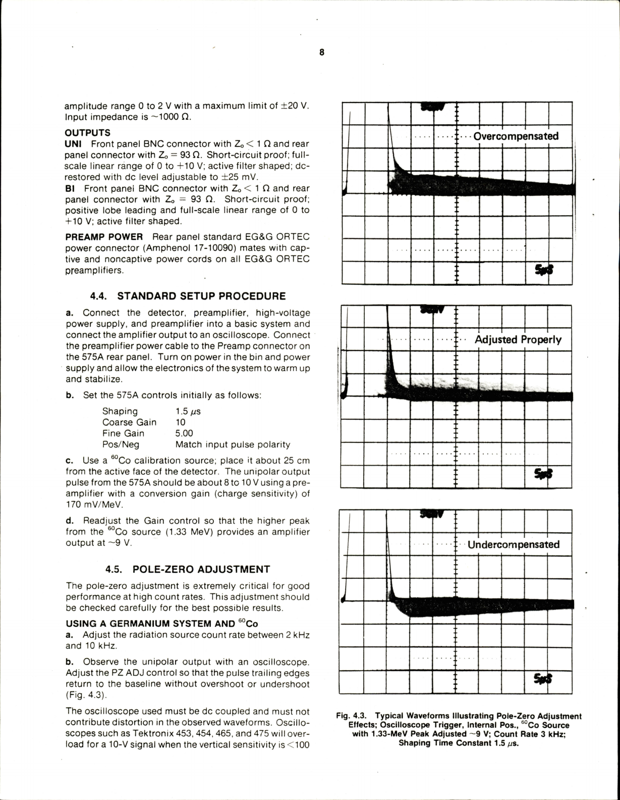
USING
A
GERMANIUM
SYSTEM
AND
^°Co
a.
Adjust
the
radiation
source
count
rate
between
2
kHz
and
10
kHz.
b.
Observe
the
unipolar
output
with
an
oscilloscope.
Adjust
the
PZ
ADJ
control
so
that
the
pulse
trailing
edges
return
to
the
baseline
without
overshoot
or
undershoot
(Fig.
4.3).
The
oscilloscope
used
must
be
dc
coupled
and
must
not
contribute
distortion
in
the
observed
waveforms.
Oscillo
scopes
such
as
Tektronix
453,454,
465,
and
475
will
over
load
for
a
10-V
signal
when
the
vertical
sensitivity
is
<100
:
-
C
verc
3mp(
insat
3d
i
^
.
I
Vdjus
ted
F
'rope
riy
i
j
:
Ur
iderc
omp
ensal
ed
J
%
r
Fig.
4.3.
Typical
Waveforms
Illustrating
Pole-Zero
Adjustment
Effects;
Oscilloscope
Trigger,
Internal
Pos.,
''°Co
Source
with
1.33-MeV
Peak
Adjusted
—9
V;
Count
Rate
3
kHz;
Shaping
Time
Constant
1.5
fjs.

FROM
AMPLIFIER
OUTPUT
IK
TO
OSCILLOSCOPE
INPUT
AAAr-
D
X
HPA
2800
SCHOTTKY
DIODES
OR
FAST
G*
DIODES
Fig.
4.4.
A
Clamp
Circuit
that
can
be
used
to
Prevent
Overloading
the
Oscilloscope
Input.
mV/cm.
To
prevent
overloading
the
oscilloscope,
use
the
clamp
circuit
shown
in
Fig.
4.4.
USING
SQUARE
WAVE
THROUGH
PREAMPLIFIER
TEST
INPUT
A
more
precise
pole-zero
adjustment
in
the
575A
can
be
obtained
by
using
a
square
wave
signal
as
the
input
to
the
preamplifier.
Many
oscilloscopes
include
a
calibration
output
on
the
front
panel,
and
this
is
a
good
source
of
square
wave
signals
at
a
frequency
of
~1
kHz.
The
ampli
fier
differentiates
the
signal
from
the
preamplifier
so
that
it
generates
output
signals
of
alternate
polarities
on
the
leading
and
trailing
edges
of
the
square
wave
input
signal,
and
these
can
be
compared
as
shown
in
Fig.
4.5
to
achieve
excellent
pole-zero
cancellation.
Use
the
following
pro
cedure:
a.
Remove
all
radioactive
sources
from
the
vicinity
of
the
detector.
Set
up
the
system
as
for
normal
operation,
including
detector
bias.
b.
Set
the
575A
controls
as
for
normal
operation;
this
includes
gain,
shaping,
and
input
polarity.
c.
Connect
the
source
of
1-kHz
square
waves
through
an
attenuator
to
the
Test
input
of
the
preamplifier.
Adjust
the
attenuator
so
that
the
575A
output
amplitude
is
~9
V.
d.
Observe
the
Unipolar
output
of
the
575A
with
an
oscil
loscope.
Adjust
the
PZ
ADJ
control
for
proper
response
according
to
Fig.
4.5.
Use
the
clamp
circuit
in
Fig.
4.4
to
prevent
overloading
the
oscilloscope
input.
4.6.
OPERATION
WITH
SEMICONDUCTOR
DETECTORS
CALIBRATION
OF
TEST
PULSER
An
EG&G
ORTEC
419
Precision
Pulse
Generator
(or
equivalent)
is
easily
calibrated
so
that
the
maximum
pulse
height
dial
reading
(1000
divisions)
is
equivalent
to
10-MeV
loss
in
a
silicon
radiation
detector.
The
procedure
is
as
follows:
a.
Connect
the
detector
to
be
used
to
the
spectrometer
system;
that
is,
preamplifier,
main
amplifier,
and
biased
amplifier.
b.
Allow
excitation
from
a
source
of
known
energy
(e.g.
alpha
particles)
to
fall
on
the
detector.
L
1
1
5
A.
PZ
Properly
Adjusted;
Slow
Trigger
to
Separate
Pulses.
1
/'
f
I
1
5
jiF.y
9.
'
•
"y
B.
Overcompensated.
1"
mmm
\
IJ
1
6
C.
Undercompensated.
Fig.
4.5.
Pole-Zero
Adjustment
Using
a
Square
Vv
to
the
Preampiifier.
J

10
c.
Adjust
the
amplifier
gain
and
the
bias
level
of
the
biased
amplifier
to
give
a
suitable
output
pulse.
d.
Set
the
pulser
Pulse
Height
control
at
the
energy
of
the
alpha
particles
striking
the
detector
(e.g.,
set
the
dial
at
547
divisions
for
a
5.47-MeV
alpha
particle
energy).
e.
Turn
on
the
pulser
and
use
its
Normalize
control
and
attenuators
to
set
the
output
due
to
the
pulser
for
the
same
pulse
height
as
the
pulse
obtained
in
step
c.
Lock
the
Normalize
control
and
do
not
move
it
again
until
recalibration
is
required.
The
pulser
is
now
calibrated;
the
Pulse
Height
dial
reads
directly
in
MeV
if
the
number
of
dial
divisions
is
divided
by
100.
AMPLIFIER
NOISE
AND
RESOLUTION
MEASURE
MENTS
As
shown
in
Fig.
4.6,
a
preamplifier,
amplifier,
pulse
generator,
oscilloscope,
and
wide-band
rms
volt
meter
such
as
the
Hewlett-Packard
3400A
are
required
for
this
measurement.
Connect
a
suitable
capacitor
to
the
input
to
simulate
the
detector
capacitance
desired.
To
obtain
the
resolution
spread
due
to
amplifier
noise:
a.
Measure
the
rms
noise
voltage
(E,ms)
at
the
amplifier
output.
b.
Turn
on
the
419
precision
pulse
generator
and
adjust
the
pulser
output
to
any
convenient
readable
voltage,
Eo,
as
determined
by
the
oscilloscope.
The
full-width-half-maximum
(FWHM)
resolution
spread
due
to
amplifier
noise
is
then
2.35
Erms
Edial
N(FWHM)
=
Co
where
Ediai
is
the
pulser
dial
reading
in
MeV,
and
2.35
is
the
factor
for
rms
to
FWHM.
For
average-responding
volt
meters
such
as
the
Hewlett-Packard
400D,
the
measured
noise
must
be
multiplied
by
1.13
to
calculate
the
rms
noise.
The
resolution
spread
will
depend
on
the
total
input
capacitance,
because
the
capacitance
degrades
the
sig-
nal-to-noise
ratio
much
faster
than
the
noise.
DETECTOR
NOISE-RESOLUTION
MEASUREMENTS
The
measurement
just
described
can
be
made
with
a
biased
detector
instead
of
the
external
capacitor
that
EG&G
ORTEC
EG&G
ORTEC
LINEAR
AMPLIFIER
OSCILLO
SCOPE
PRE
AMP
.
DETECTOR
.
OR
CAPACITOR
EG&G
ORTEC
PULSE
GENERATOR
VOLTMETER
would
be
used
to
simulate
detector
capacitance.
The
resolution
spread
will
be
larger
because
the
detector
contributes
both
noise
and
capacitance
to
the
input.
The
detector
noise-resolution
spread
can
be
isolated
from
the
amplifier
noise
spread
if
the
detector
capacitance
is
known,
since
(Ndet)^
+
(Nelec)'
-
(N,o,al)^
where
Ntoiai
is
the
total
resolution
spread,
and
Neiec
is
the
electronic
resolution
spread
when
the
detector
is
re
placed
by
its
equivalent
capacitance.
The
detector
noise
tends
to
increase
with
bias
voltage,
while
the
detector
capacitance
decreases.
The
net
change
in
resolution
spread
will
depend
upon
which
effect
is
dominant.
Figure
4.7
shows
curves
of
typical
noise-resolution
spread
versus
bias
voltage
using
data
from
several
EG&G
ORTEC
silicon
surface-barrier
semi
conductor
radiation
detectors.
A
-
EG4G
ORTEC
BA-030-007-300
B
-
EG&G
ORTEC
BA-025-050-100
—
0
-
EG&G
ORTEC
BA-025-100-100
D
-
EG&G
ORTEC
BA-030-2PO-100
E
-
EG&G
ORTEC
SA-045-450-100
100159
50
75
Bias
Voltagt
125
Fig.
4.6.
System
for
Measuring
Amplifier
and
Detector
Noise
Resolution.
Fig.
4.7.
Noise
as
a
Function
of
Bias
Voltage.
AMPLIFIER
NOISE-RESOLUTION
MEASUREMENTS
USING
MCA
Probably
the
most
convenient
method
of
making
resolution
measurements
is
with
a
pulse
height
analyzer,
as
shown
by
the
setup
illustrated
in
Fig.
4.8.
The
electronic
noise-resolution
spread
can
be
measured
directly
with
a
pulse
height
analyzer
and
the
mercury
pulser
as
follows:
a.
Select
the
energy
of
interest
with
an
EG&G
ORTEC
419
Precision
Pulse
Generator.
Set
the
amplifier
and
biased
amplifier
gain
and
bias
level
controls
so
that
the
energy
is
in
a
convenient
channel
of
the
analyzer.
b.
Calibrate
the
analyzer
in
keV
per
channel,
using
the
pulser:
full
scale
on
the
pulser
dial
is
10
MeV
when
cali
brated
as
described
above.
c.
Obtain
the
amplifier
noise-resolution
spread
by
measuring
the
FWHM
of
the
pulser
peak
in
the
spectrum.
The
detector
noise-resolution
spread
for
a
given
detector
bias
can
be
determined
in
the
same
manner
by
connect
ing
a
detector
to
the
preamplifier
input.
The
amplifier

11
DETECTOR
CAPACITOR
-|
I
EG&G
I
j
ORTEC
j
I
GATED
BIAS
I
I
AMPLIFIER
I
L-
J
EG&G
ORTEC
PULSE
GENERATOR
MULTI
CHANNEL
PULSE
HEIGHT
ANALYZER
EG&G
ORTEC
PULSE
STRETCHER
EG&G
ORTEC
BIASED
AMPLIFIER
EG&G
ORTEC
LINEAR
AMPLIFIER
EG&G
ORTEC
Fig.
4.8.
System
for
Measuring
Resolution
with
a
Pulse
Height
Analyzer.
noise-resolution
spread
must
be
subtracted
as
described
in
"Detector
Noise-Resoiution
Measurements."
The
de
tector
noise
will
vary
with
detector
size
and
bias
condi
tions
and
possibly
with
ambient
conditions.
CURRENT
VOLTAGE
MEASUREMENTS
FOR
Si
AND
Ge
DETECTORS
The
amplifier
system
is
not
directly
involved
in
semiconductor
detector
current
voltage
measurements,
but
the
amplifier
serves
to
permit
noise
monitoring
during
the
setup.
The
detector
noise
meas
urement
is
a
more
sensitive
method
than
a
current
measurement
of
determining
the
maximum
detector
volt
age
that
should
be
used
because
the
noise
increases
more
rapidly
than
the
reverse
current
at
the
onset
of
detector
breakdown.
Make
this
measurement
in
the
absence
of
a
source.
Figure
4.9
shows
the
setup
required
for
current
voltage
measurements.
An
EG&G
ORTEC
428
Bias
Supply
is
used
as
the
voltage
source.
Bias
voltage
should
be
ap-
I
MICRO
I
AMMETER
j
DETECTOR
BIAS
SUPPLY
Currant
Monitorino
Jacks
EG&G
ORTEC
EG&G
ORTEC
RMS
VOLTMETER
LINEAR
AMPLIFIER
PREAMP
DETECTOR
Normal
Circuit
MICRO
AMMETER
/•
BYPASS
^
CAPACITOR
plied
slowly
and
reduced
when
noise
increases
rapidly
as
a
function
of
applied
bias.
Figure
4.10
shows
several
typical
current
voltage
curves
for
EG&G
ORTEC
silicon
surface-barrier
detectors.
When
it
is
possible
to
float
the
microammeter
at
the
detec
tor
bias
voltage,
the
method
of
detector
current
measure
ment
shown
by
the
dashed
lines
in
Fig.
4.9
is
preferable.
The
detector
is
grounded
as
in
normal
operation,
and
the
microammeter
is
connected
to
the
current
monitoring
jack
on
the
428
detector
bias
supply.
A
-
EG&G
ORTEC
BA-030-007-300
B
-
EG&G
ORTEC
BA-025-050-100
0
-
EG&G
ORTEC
BA-025-100-100
D
-
EG&G
ORTEC
BA-030-200-100
E
-
EG&G
ORTEC
BA-045-450-100
Fig.
4.9.
System
for
Detector
Current
and
Voltage
Measurements.
40
60
Bias
Voltage
Fig.
4.10.
Silicon
Detector
Back
Current
vs
Bias
Voltage.
4.7.
OPERATION
IN
SPECTROSCOPY
SYSTEMS
HIGH-RESOLUTION
ALPH-PARTICLE
SPECTROS
COPY
SYSTEM
The
block
diagram
of
a
high-resolution
spectroscopy
system
for
measuring
natural
alpha
particle
radiation
is
shown
in
Fig.
4.11.
Since
natural
alpha
radi
ation
occurs
only
above
several
MeV,
an
EG&G
ORTEC
444
Biased
Amplifier
is
used
to
suppress
the
unused
por
tion
of
the
spectrum;
the
same
result
can
be
obtained
by
using
digital
suppression
on
the
MCA
in
many
cases.
Alpha-particle
resolution
is
obtained
in
the
following
manner:
a.
Use
appropriate
amplifier
gain
and
minimum
biased
amplifier
gain
and
bias
level.
Accumulate
the
alpha
peak
in
the
MCA.
b.
Slowly
increase
the
bias
level
and
biased
amplifier
gain
until
the
alpha
peak
is
spread
over
5
to
10
channels
and
the
minimum-
to
maximum-energy
range
desired
corresponds
to
the
first
and
last
channels
of
the
MCA.
c.
Calibrate
the
analyzer
in
keV
per
channel
using
the
pulserand
the
known
energy
of
the
alpha
peak
(see
"Cali
bration
of
Test
Pulser")
or
two
known-energy
alpha
peaks.
d.
Calculate
the
resolution
by
measuring
the
number
of
channels
at
the
FWHM
level
in
the
peak
and
converting
this
to
keV.
HIGH-RESOLUTION
GAMMA
SPECTROSCOPY
SYSTEM
A
high-resolution
gamma
spectroscopy
sys
tem
block
diagram
is
shown
in
Fig.
4.12.
Although
a
biased
amplifier
is
not
shown
(an
analyzer
with
more
channels
being
preferred),
it
can
be
used
if
the
only
ana
lyzer
available
has
fewer
channels
and
only
higher
ener
gies
are
of
interest.

12
(—
DETECTOR
To
Vacuum
Pump
—a
VACUUM
CHAMBER
EG&G
ORTEC
ORTEC
ORTEC
GATED
PREAMP
BIASED
EG&G
ORTEC
DETECTOR
BIAS
SUPPLY
EG&G
ORTEC
PULSE
GENERATOR
EG&G
ORTEC
MULTI
CHANNEL
PULSE
HEIGHT
ANALYZER
OSCILLO
SCOPE
NOISE
METER
Fig.
4.11.
System
for
High-Resolution
Alpha-Particle
Spectroscopy.
GERMANIUM
DETECTOR
and
CRYOSTAT
EG&G
ORTEC
EG&G
ORTEC
LINEAR
AMPLIFIER
EG&G
ORTEC
PULSE
HEIGHT
ANALYZER
EG&G
ORTEC
PULSE
GENERATOR
EG&G
ORTEC
HIGH-
VOLTAGE
BIAS
SUPPLY
OSCILLO
SCOPE
NOISE
METER
Fig.
4.12.
System
for
High-Resolution
Gamma
Spectroscopy.
in
Fig.
4.13.
The
amplifier
shaping
time
constants
should
be
selected
In
the
region
of
0.5
to
1.5/iS
for
Nal
or
plastic
sclntillators.
For
scintillators
having
longer
decay
times,
longer
time
constants
should
be
selected.
X-RAY
SPECTROSCOPY
USING
PROPORTIONAL
COUNTERS
Space
charge
effects
In
proportional
counters,
operated
at
high
gas
amplification,
tend
to
degrade
the
resolution
capabilities
drastically
at
x-ray
energies,
even
at
relatively
low
counting
rates.
By
using
a
high-gain,
low-noise
amplifying
system
and
lower
gas
amplification,
these
effects
can
be
reduced
and
a
con
siderable
improvement
in
resolution
can
be
obtained.
The
block
diagram
in
Fig.
4.14
shows
a
system
of
this
type.
Analysis
can
be
accomplished
by
simultaneous
acquisi
tion
of
all
data
on
a
multichannel
analyzer
or
counting
a
region
of
interest
In
a
single-channel
analyzer
window
with
a
counter
and
timer
or
counting
ratemeter.
When
a
germanium
detector
that
Is
cooled
by
a
liquid
nitrogen
cryostat
is
used,
it
Is
possible
to
obtain
reso
lutions
from
about
1
keV
FWHM
up
(depending
on
the
energy
of
the
incident
radiation
and
the
size
and
quality
of
the
detector).
Reasonable
care
Is
required
to
obtain
such
results.
Some
guidelines
for
obtaining
optimum
resolution
are:
a.
Keep
Interconnection
capacitance
between
the
de
tector
and
preamplifier
to
an
absolute
minimum
(no
long
cables).
b.
Keep
humidity
low
near
the
detector-preamplifier
junction.
c.
Operate
the
amplifier
with
the
shaping
time
that
pro
vides
the
best
signal-to-noise
ratio.,
d.
Operate
at
the
highest
allowable
detector
bias
to
keep
the
Input
capacitance
low.
SCINTILLATION-COUNTER
GAMMA
SPECTROS
COPY
SYSTEMS
The
EG&G
ORTEC
575A
can
be
used
in
scintillation-counter
spectroscopy
systems
as
shown
EG&G
ORTEC
HIGH
VOLTAGE
POWER
SUPPLY
SCINTILLATION
COUNTER
EG&G
ORTEC
PULSE
GENERATOR
EG&G
ORTEC
EG&G
SCINTIL
ORTEC
MULTICHANNEL
LINEAR
PULSE
HEIGHT
LATION
COUNTER
AMPLIFIER
ANALYZER
PREAMPLIFIER
Fig.
4.13.
Scintitlation-Counter
Gamma
Spectroscopy
System.

13
To
Counting
Ratemeter
or
Counter
and
Timer
PROPORTIONAL
COUNTER
EG&G
ORTEC
LINEAR
AMPLIFIER
PULSE
GENERATOR
EG&G
ORTEC
EG&G
ORTEC
PRO
PORTIONAL
COUNTER
PREAMPLIFIER
EG&G
ORTEC
HIGH
VOLTAGE
POWER
SUPPLY
EG&G
ORTEC
SINGLE
CHANNEL
ANALYZER
MULTICHANNEL
PULSE
HEIGHT
ANALYZER
4.8.
OTHER
EXPERIMENTS
Block
diagrams
Illustrating
how
the
575A
and
other
EG&G
ORTEC
modules
can
be
used
for
experimental
setups
for
various
other
applications
are
shown
In
Figs.
4.15, 4.16,
and
4.17.
Fig.
4.14.
High-Resolution
X-Ray
Energy
Analysis
System
Using
a
Proportional
Counter.
Linear
Output
to
Multichannel
Analyzer
SILICON
SURFACE
^
^
BARRIER
DETECTOR
Source
□
GERMANIUM
DETECTOR
EG&G
ORTEC
DELAY
AMPLIFIER
EG&G
ORTEC
TIMING
FILTER
AMPLIFIER
EG&G
ORTEC
LINEAR
AMPLIFIER
EG&G
ORTEC
FAST
COINCIDENCE
UNIT
EG&G
ORTEC
CFT
DISCRIMI
NATOR
PR
6
AMP
EG&G
ORTEC
EG&G
ORTEC
GATED
BIASED
AMPLIFIER
EG&G
ORTEC
GATE
&
DELAY
GENERATOR
EG&G
ORTEC
TIMING
SCA
EG&G
ORTEC
LINEAR
AMPLIFIER
PREAMP
Fig.
4.15.
Gamma-Ray
Charged-Partlcle
Coincidence
Experiment.

14
EG&G
ORTEC
SCINTIL
LATION
PREAMP
EG&G
ORTEC
LINEAR
amplifier
ORTEC
P.M.
TUBE
&
BASE
EG&G
ORTEC
CFT
DISCRIMI
NATOR
EG&G
ORTEC
GATE&
DELAY
GENERATOR
GERMANIUM
DETECTOR
EG&G
ORTEC
Nai
EG&G
ORTEC
PREAMP
TIMING
FILTER
AMPLIFIER
EG&G
ORTEC
LINEAR
P.M.
1
AMPLIFIER
TUBE
BASE
EG&G
ORTEC
EG&G
ORTEC
EG&G
ORTEC
SCINTIL
LATION
TIMING
SCA
LINEAR
AMPLIFIER
200330a
PREAMP
EG&G
ORTEC
FAST
COINCIDENCE
UNIT
EG&G
ORTEC
DELAY
AMPLIFIER
I
EG&G
ORTEC
GATED
BIASED
AMPLIFIER
Linear
Output
to
Multichannel
Analyzer
Fig.
4.16.
Gamma-Ray
Pair
Speclrometry.
ORTEC
ORTEC
SCINTIL
LATION
PREAMP
L
NEAR
AMPLIFIER
TUBE
EG&G
ORTEC
TIMING
SCA
I
I
GERMANIUM
'
'
'
DETECTOR
EG&G
ORTEC
200329
a
EG&G
ORTEC
CFT
DISCRIMI
EG&G
NATOR
ORTEC
GATE
&
DELAY
GENERATOR
EG&G
ORTEC
TIMING
FILTER
AMPLIFIER
EG&G
EG&G
ORTEC
GATED
BIASED
AMPLIFIER
COINCIDENCE
Linear
Output
to
Multichannel
Analyzer
LINEAR
amplifier
EG&G
ORTEC
DELAY
AMPLIFIER
Fig.
4.17.
Gamma-Gamma
Coincidence
Experiment.
Table of contents
Other EG&G Amplifier manuals

EG&G
EG&G ORTEC 113 Service manual

EG&G
EG&G ORTEC 535 Service manual

EG&G
EG&G ORTEC 118A User manual

EG&G
EG&G ORTEC 427 User manual

EG&G
EG&G ORTEC 444 User manual

EG&G
EG&G ORTEC 474 Service manual

EG&G
EG&G 128A Service manual

EG&G
EG&G 113 Service manual

EG&G
EG&G ORTEC 452 User manual

EG&G
EG&G ORTEC 572 Service manual


