EG&G ORTEC 535 Service manual
n
Model
535
Quad
Fast
Amplifier
Operating
and
Service
Manual

Model
535
Quad
Fast
Amplifier
Operating
and
Service
Manual
This
manual
applies
to
instruments
marked
"Rev
05"
on
rear
panel
Printed
in
U.S.A.
ORTEC
Part
Number
678820
3348
0.5C
1186

standard
Warranty
for
EG&G
ORTEC
Nuclear
Eiectronic
Instruments
EG&G
ORTEC
warrants
that
the
items
will
be
delivered
free
from
defects
in
material
or
workmanship.
EG&G
ORTEC
makes
no
other
warranties,
express
or
implied,
and
specifically
NO
WARRANTY
OF
MERCHANTABILITY
OR
FITNESS
FOR
A
PARTICULAR
PURPOSE.
EG&G
ORTEC's
exclusive
liability
is
limited
to
repairing
or
replacing
at
EG&G
ORTEC's
option,
items
found
by
EG&G
ORTEC
to
be
defective
in
workmanship
or
materials
within
two
years
from
the
date
of
delivery.
EG&G
ORTEC's
liability
on
any
claim
of
any
kind,
including
negligence,
loss
or
damages
arising
out
of,
connected
with,
or
from
the
performance
or
breach
thereof,
or
from
the
manufacture,
sale,
delivery,
resale,
repair,
oruseof
any
item
or
services
covered
by
this
agree
ment
or
purchase
order,
shall
in
no
case
exceed
the
price
allocable
to
the
item
or
service
furnished
or
any
part
thereof
that
gives
rise
to
the
claim.
In
the
event
EG&G
ORTEC
fails
to
manufacture
or
deliver
items
called
for
In
this
agreement
or
pur
chase
order,
EG&G
ORTEC's
exclusive
liability
and
buyer's
exclusive
remedy
shall
be
release
of
the
buyer
from
the
obliga
tion
to
pay
the
purchase
price.
In
no
event
shall
EG&G
ORTEC
be
liable
for
special
or
consequential
damages.
Quality
Control
Before
being
approved
for
shipment,
each
EG&G
ORTEC
nuclear
electronic
instrument
must
pass
a
stringent
set
of
quality
control
tests
designed
to
expose
any
flaws
in
materials
or
workmanship.
Permanent
records
of
these
tests
are
maintained
for
use
in
warrany
repair
and
as
a
source
of
statistical
information
for
design
improvements.
Repair
Service
If
It
becomes
necessary
to
return
this
instrument
for
repair,
it
is
essential
that
Customer
Services
be
contacted
in
advance
of
its
return
so
that
a
Return
Authorization
Number
can
be
assigned
to
the
unit.
Also,
EG&G
ORTEC
must
be
informed,
either
in
writing,
by
telephone
[(615)
482-4411]
or
by
telex
(55-7450)
of
the
nature
of
the
fault
of
the
instrument
being
re
turned
and
of
the
model,
serial,
and
revision
("Rev"
on
rear
panel)
numbers.
Failure
to
do
so
may
cause
unnecessary
delays
In
getting
the
unit
repaired.
The
EG&G
ORTEC
standard
procedure
requires
that
instruments
returned
for
repair
pass
the
same
quality
control
tests
that
are
used
for
new-production
instruments.
Instruments
that
are
returned
should
be
packed
so
that
they
will
withstand
normal
transit
handling
and
must
be
shipped
PREPAID
via
Air
Parcel
Post
or
United
Parcel
Service
to
the
nearest
EG&G
ORTEC
repair
center.
(In
the
case
where
the
Instrument
did
not
function
upon
pur
chase,
EG&G
ORTEC
will
pay
shipment
costs
both
ways.)
The
address
labei
and
the
package
should
include
the
Return
Authorization
Number
assigned.
Instruments
being
returned
that
are
damaged
in
transit
due
to
inadequate
packing
will
be
repaired
at
the
sender's
expense,
and
it
will
be
the
sender's
responsibility
to
make
claim
with
the
shipper.
Instruments
not
in
warranty
will
be
repaired
at
the
standard
charge
unless
they
have
been
grossly
misused
or
mishandled,
in
which
case
the
user
will
be
notified
prior
to
the
repair
being
done.
A
quotation
will
be
sent
with
the
notification.
Damage
in
Transit
Shipments
should
be
examined
immediately
upon
receipt
for
evidence
of
external
or
concealed
damage.
The
carrier
making
delivery
should
be
notified
immediately
of
any
such
damage,
since
the
carrier
is
normally
liable
for
damage
in
shipment.
Packing
materials,
waybills,
and
other
such
documentation
should
be
preserved
in
order
to
establish
claims.
After
such
notification
to
the
carrier,
please
notify
EG&G
ORTEC
of
the
circumstances
so
that
assistance
can
be
provided
in
making
damage
claims
and
in
providing
replacement
equipment
if
necessary.

Ill
CONTENTS
Page
WARRANTY
ij
PHOTOGRAPH
iv
1.
DESCRIPTION
1
2.
SPECIFICATIONS
'
. .
1
2.1.
Performance
1
2.2.
Controls
1
2.3.
Electrical
and
Mechanical
1
3.
INSTALLATION
2
3.1.
Connection
to
Detector
2
3.2.
Connection
of
Output
2
3.3.
Cascading
2
4.
OPERATING
INSTRUCTIONS
;
2
5.
CIRCUIT
DESCRIPTION
2
6.
MAINTENANCE
AND
CALIBRATION
3
6.1.
Preventive
Maintenance
3
6.2.
Corrective
Maintenance
3
6.3.
Calibration
3
6.4.
Factory
Repair
3
Schematic
635120

I
m
P!

EG&G
ORTEC
MODEL
535
QUAD
FAST
AMPLIFIER
1.
DESCRIPTION
The
EG&G
ORTEC
535
Quad
Fast
Amplifiercontainsfour
independent
direct-coupled
amplifiers
packaged
in
a
single-width
NIM
module.
Each
section
has
variable
voltage
gain,
5-10,
and
can
drive
±5
V
into
a
50fi
load.
The
excellent
dc
and
gain
stabilities
allow
cascading
sections
to
achieve
a
total
voltage
gain
of
10,000.
The
535
features
high
bandwidth
and
wide
dynamic
range,
<3
ns
rise
and
fall
times
to
±5
V,
coupled
with
low
noise
and
fast
overload
recovery.
Input
overload
pro
tection
is
provided
for
each
channel.
Hybrid
circuit
technology
gives
the
535
higher
reliability
In
an
economical,
high-density
package.
For
operator
convenience
independent
bandwidth
(BDW),
output
dc
offset
(DC),
and
fine
gain
(GAIN)
adjustments
are
In
cluded.
The
535
Quad
Fast
Amplifier
is
ideally
suited
to
precede
discriminators,
linear
gates,
fast
current
integrators,
or
any
instrument
requiring
fast
linear
input
signals.
The
low
noise
characteristics
of
the
535
make
it
particularly
useful
in
photon
counting
and
fast-timing
applications.
2.
SPECIFICATIONS
2.1.
PERFORMANCE
NOMINAL
VOLTAGE
GAIN
5-10;
noninverting.
RISE
TIME
<3
ns
to
±5
V
into
50
O;
bandwidth
>120
MHz.
NOISE
<25
//V
referred
to
the
input
measured
with
an
HP3400A
true
rms
voltmeter.
Wideband
noise
(200
MHz)
<30
A(V
referred
to
the
input.
INTEGRAL
NONLINEARITY
Typically
<±1%foroutput
to
±5
V.
PULSE
OVERLOAD
RECOVERY
Typically
<5
ns
for
a
X10
overload.
GAIN
INSTABILITY
Typically
<±0.05%/°
C.
DC
INSTABILITY
Typically
<±150
uVfC
referred
to
the
output.
INPUT
IMPEDANCE
50
O,
dc-coupled.
OUTPUT
IMPEDANCE
<1
Q,
dc-coupled.
OUTPUT
LINEAR
RANGE
±5
V
Into
50
O.
OPERATING
TEMPERATURE
RANGE
0
to
50°
C.
CROSSTALK
<0.02%
between
output
of
one
channel
and
input
of
another
channel.
2.2.
CONTROLS
BDW
20-turn
potentiometer
adjusts
the
output
band
width
and
overshoot.
Front
panel
mounted.
DC
20-turn
potentiometer
adjusts
the
output
dc
offset.
Front
panel
mounted.
GAIN
20-turn
potentiometer
adjusts
the
voltage
gain
from
typically
5
to
10.
Front
panel
mounted.
2.3.
ELECTRICAL
AND
MECHANICAL
POWER
REQUIRED
+24
V,
83
mA;-24
V,
83
mA;+12
V,
167
mA;
-12
V,
167
mA.
WEIGHT
Net
0.32
kg
(12
oz).
Shipping
1.25
kg
(2
lb
12
oz).
DIMENSIONS
3.81
x
6.1
x
8.89
cm
(1.5
x
2.4
x
3.5
in.).

3.
INSTALLATION
3.1.
CONNECTION
TO
DETECTOR
Connect
the
output
from
the
detector
or
preamplifier
to
the
Input
BNC
on
the
535
with
50
O
coaxial
cable.
This
cable
should
be
as
short
as
practical
to
minimize
the
physical
distance
through
which
the
detector
output-
current
pulse
has
to
pass.
The
amount
of
noise
that
will
be
added
to
the
signal
increases
with
cable
length.
An
input
signal
to
the
535
can
be
of
either
polarity
(e.g.,
it
can
originate
from
the
anode
or
any
dynode
in
a
photo-
multiplier
tube
circuit).
AC-coupiing
must
be
used
to
pre
vent
any
high
voltage
from
the
detector
being
applied
directly
to
the
535
input.
An
input-protection
circuit
is
included
which
allows
excellent
(typically
<5
ns)
over
load
recovery.
The
output
signal
from
the
535
will
have
the
same
polarity
as
the
input
and
will
be
amplified
by
a
factor
of
5-10.
The
linear
output
range
is
±5
V
into
a
50
n
load.
the
535
through
50
O
cable
terminated
by
a
50
Q
load.
If
the
driving
instrujnent
does
not
have
an
input
imped
ance
of
50
n,
an
external
terminating
resistor
should
be
added
to
prevent
pulse
reflections.
3.3.
CASCADING
When
an
amplification
greater
than
a
factor
of
10
is
de
sired,
the
input
signal
can
be
cascaded
through
additional
sections
of
the
535.
Each
section
provides
the
nominal
maximum
gain
of
10.
Cascading
the
signal
through
all
four
sections
will
provide
an
amplification
factor
of
about
10,000.
When
cascading
sections
of
the
535,
care
must
be
taken
to
ensure
proper
adjustment
of
the
DC
offset
controls
to
ensure
operation
within
the
linear
range
of
±5
V.
3.2.
CONNECTION
OF
OUTPUT
The
output
impedance
of
the
535
is
nominally
1
O.
Any
counter,
amplifier,
or
timing
instrument
can
be
driven
by
4.
OPERATING
INSTRUCTIONS
Three
operator
controls
(DC,
Gain,
and
BDW)
are
pro
vided
on
the
535.
The
DC
adjustment
permits
the
setting
of
the
dc-output
offset
to
zero
volts.
[The
input
offset
voltage
is
adjusted
by
an
internal
potentiometer
mounted
on
a
printed
wiring
board
(PWB).]
The
Gain
potentiom
eter
adjusts
voltage
gain
continuously
from
5
to
10.
The
BDW
(bandwidth)
sets
the
rise
time
or
overshoot
appro
priate
for
the
experiment.
The
tilt
is
adjusted
by
an
internal
potentiometer
mounted
on
the
PWB.
5.
CIRCUIT
DESCRIPTION
The
circuit
of
the
535
Quad
Fast
Amplifier
is
shown
in
schematic
635120
at
the
back
of
this
manual.
Refer
to
this
schematic
for
the
following
circuit
description.
Since
ail
four
channels
of
the
535
are
identical,
only
channel
1
will
be
discussed.
Diodes
D1
and
D2
form
a
bridge
current
limiter
which
is
voltage-clamped
by
01
and
Q2
to
limit
the
input
swing
to
'K.
W.
Renner,
M.
O.
Bedwell,
and
J.
F.
Pierce,
"A
Wideband
Direct
Coupled
Amplifier
Utilizing
a
Fast/Slow
Loop
Concept,"
IEEE
Trans.
Nucl.
Sci.,
NS-28(1),
584.
^K.
W.
Renner,
4
Direct
Coupled
Wideband
Hybridized
Amplifier
with
a
Fast/Slow
Loop,
M.A.
Thesis,
University
of
Tennessee,
Knoxville,
December
1980.
the
hybrid
fast
amplifier,
A1.
This
input
protection
cir
cuitry
ensures
that
no
harsh
overload
signals
will
reach
A1,
thus
offering
excellent
overload
recovery
time.
Voltage
gain
is
varied
by
adjusting
resistor
R2.
The
input
offset
voltage
is
adjusted
by
resistor
R4
which
controls
the
current
in
the
current
limiting
bridge.
The
fast
amplifier
hybrid
uses
a
fast/slow
loop
tech
nique.''^
The
input
signal
enters
the
slow
loop
on
pin
14
of
A1
and
is
ac-coupled
through
C2
and
C3
to
the
fast
loop
input
on
pin
1
of
A1.
The
slow-loop
gain
is
adjusted
by
resistor
R9.
The
adjustment
is
factory-set
so
that
the
fast
signal
gain
equals
the
do
gain.
The
fast
amplifier
band
width
is
controlled
by
resistorRIB.
The
slow
loop
controls
the
dc-output
offset
which
is
adjusted
by
R12.
6.
MAINTENANCE
AND
CALIBRATION
6.1.
PREVENTIVE
MAINTENANCE
Give
reasonable
attention
to
mechanical
details.
Keep
the
signal
connectors
clean
at
all
times.
Periodically
remove
the
cover
and
inspect
the
interior
of
the
module
for
dust
accumulation
or
other
undesirable
conditions.
Glean
as
often
as
required
by
local
conditions
(normally
about
once
every
12
months).
6.2.
CORRECTIVE
MAINTENANCE
Corrective
maintenance
generally
consists
of
replacing
defective
components
(i.e.,
resistors,
capacitors,
diodes,
transistors,
and
integrated
circuits),
replacing
missing
hardware,
and
tightening
loose
hardware.
Do
not
use
excessive
force
when
tightening
screws
or
nuts.
When
replacing
components
on
a
PWB,
be
sure
that
the
board
is
not
damaged
by
excessive
heating.
When
un
soldering
leads,
grip
the
lead
that
is
to
be
removed
with
pliers
or
some
similar
tool
that
acts
as
a
heat
sink.
Heat
the
solder
joint
as
little
as
possible
while
maintaining
a
steady
pull
on
the
lead
to
assure
its
prompt
removal.
Remove
excess
solder
from
the
board
with
a
solder-puller.
Do
not
redrill
holes
in
the
PWB
since
many
are
plated
through
the
board.
If
the
integrity
of
a.
plated-through
hole
is
in
doubt,
solder
the
component
lead
on
both
sides
of
the
board.
When
a
defective
component
is
to
be
removed
from
a
PWB,
the
preferred
method
is
to
cut
both
or
all
leads
to
the
component
and
then
remove
each
of
the
leads
from
the
board.
6.3.
CALIBRATION
Follow
this
procedure
to
adjust
all
controls
of
each
channel
of
the
535.
Since
all
four
channels
are
identical,
only
channel
1
will
be
discussed.
1.
Furnish
power
to
the
unit
for
at
least
ten
minutes.
2.
Use
50
O
cable
to
connect
the
In
connector
of
the
535
to
a
digital
voltmeter.
Adjust
R4
(mounted
on
the
PWB)
as
needed
to
set
the
input
dc
level
at
0
V
±
1
mV.
3.
Use
50
Q
cable
to
connect
the
Out
connector
of
the
535
to
a
digital
voltmeter.
No
connection
should
be
made
to
the
In
connector.
Adjust
R12
(front
panel)
as
needed
to
set
the
Out
dc
level
at
0
V
±
1
mV.
4.
Using
50
O
cable,
connect
a
1
ns
rise
time
pulser
(HP215A
Pulser
or.equivalent)
to
an
oscilloscope
with
a
500
MHz
bandwidth
(Tektronix
7904
mainframe
and
7A19
vertical
plug-in
unit
or
equivalent).
Set
the
oscilloscope
input
impedance
to
50
Cl.
Adjust
the
HP215A
output
to
-500
mV.
5.
Using
50
O
cable,
connect
the
output
of
the
pulser
to
the
In
connector
of
the
535.
Oonnect
the
Out
connector
of
the
535
to
the
500
MHz
oscilloscope.
Set
the
oscillo
scope
input
impedance
to
50
Q.
Adjust
the
Gain
(front
panel)
potentiometer
of
the
535
to
produce
a
-5
V
output
signal.
Adjust
the
BDW
(front
panel)
potentiometer
of
the
535
to
produce
a
3.1
ns
rise
time
signal.
This
sets
the
rise
time
of
the
535
to
3.0
ns.
6.
Reverse
the
polarity
of
the
pulser
and
repeat
steps
4
and
5
for
positive
signals.
7.
Set
the
oscilloscope
Oal
output
to
some
convenient
value
such
as
1
kHz,
0.4
V.
Set
the
oscilloscope
vertical
input
to
DO.
Observe
the
oscilloscope
Oal
signal
which
should
be
a
square
wave.
Using
50
O
cable,
connect
the
Oal
signal
to
the
535
In
connector.
Using
50
Q
cable,
connect
the
535
Out
connector
to
the
oscilloscope
input.
Adjust
R9
(mounted
on
the
PWB),
the
Tilt
Adj,
as
needed
to
produce
a
square
wave
output
from
the
535.
The
ad
justment
of
R9
equalizes
the
gain
of
the
fast
loop
and
the
slow
loop
within
the
hybrid
amplifier
A1.
6.4.
FACTORY
REPAIR
This
instrument
can
be
returned
to
the
EG&G
ORTEO
factory
for
service
and
repair
at
a
nominal
cost.
Our
standard
procedure
for
repair
ensures
the
same
quality
control
and
checkout
that
are
used
for
a
new
instrument.
Always
contact
the
Oustomer
Services
Department
at
EG&G
ORTEO,
(615)
482-4411,
before
sending
in
an
instrument
for
repair
to
obtain
shipping
instructions
and
so
that
the
required
Return
Authorization
Number
can
be
assigned
to
the
unit.
Write
this
number
on
the
address
label
and
on
the
package
to
ensure
prompt
attention
when
it
reaches
the
EG&G
ORTEO
factory.

BIN/MODULE
CONNECTOR
PIN
ASSIGNMENTS
FOR
AEC
STANDARD
NUCLEAR
INSTRUMENT
MODULES
PER
TID-20893
(Rev
4)
(adopted
by
DOE)
Pin
Function
Pin
Function
1
+3
volts
23
Reserved
2
-3
volts
24
Reserved
3
Spare
Bus
25
Reserved
4
Reserved
Bus
26
Spare
5
Coaxial
27
Spare
6
Coaxial
•28
+24
volts
7
Coaxial
•29
-24
volts
8
200
volts
dc
30
Spare
Bus
9
Spare
31
Spare
•10
+6
volts
32
Spare
•11
-6
volts
•33
117
volts
ac
(Hot)
12
Reserved
Bus
•34
Power
Return
Ground
13
Spare
••35
Reset
(Sealer)
14
Spare
••36
Gate
15
Reserved
"37
Reset
(Auxiliary)
•16
,+12
volts
38
Coaxial
•17
-12
volts
39
Coaxial
18
Spare
Bus
40
Coaxial
19
Reserved
Bus
•41
117
volts
ac
(Neut.)
20
Spare
•42
High
Quality
Ground
21
Spare
G
Ground
Guide
Pin
22
Reserved
Pins
marked
(*)
are
installed
and
wired
in
EG&G
ORTEC's
4001A. 40018.
4001C.
401A.
and
4018
Modular
System
8ins.
Pins
marked
(*)
and
(")
are
installed
in
EG&G
ORTEC-HEP
M250/N
and
M350/N
NIM8INS.
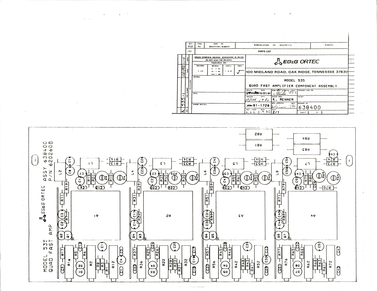
MODEL
535
ORTEC
QUAD
FAST
AMP
ASSY
63840C
P/N
6202605
rw)
—j
Ri7
R26[-
H
R21
h
rrra
(ci
C
C37)
—I
R57
I—
H
R51
-
H
R45t-
H
RA6h-
CC2^
(C3
rgrr>
R77t-
("^)
(c^fcts^
—i
r7i
[-
R79F
R62
—
R6d
—
—
o:
—
R63
-
fC5i
—I
R61
I—
R72
CE53
rcT^
ro
CD
CD
c
CC
535-1
:iMM
7X1//
r|.'
■
-
J
3
05
OJ
J
00
I
o
o
■n
3
o
m
o
»
m
r
n
o
cn
3
C4
■0
cn
o
:
=
-
I
{
S
•
2
'
ES
?!
E"
Pi
C]
s
ttw
Table of contents
Other EG&G Amplifier manuals

EG&G
EG&G ORTEC 474 Service manual

EG&G
EG&G ORTEC 485 User manual

EG&G
EG&G 128A Service manual

EG&G
EG&G ORTEC 113 Service manual

EG&G
EG&G ORTEC 427 User manual

EG&G
EG&G 113 Service manual

EG&G
EG&G ORTEC 118A User manual

EG&G
EG&G ORTEC 452 User manual

EG&G
EG&G ORTEC 444 User manual

EG&G
EG&G ORTEC 414A Service manual


