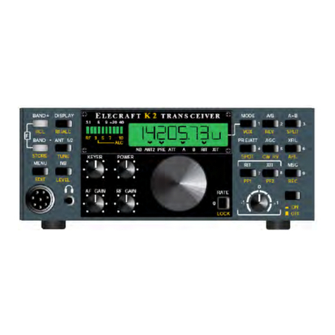
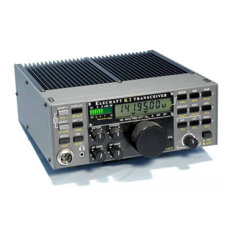
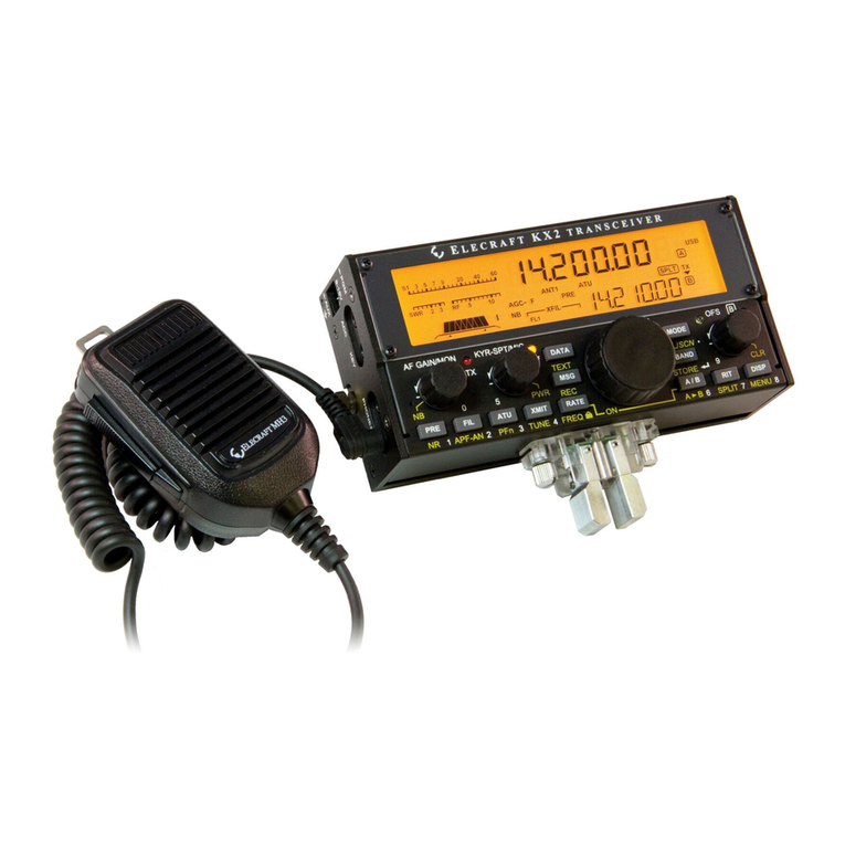
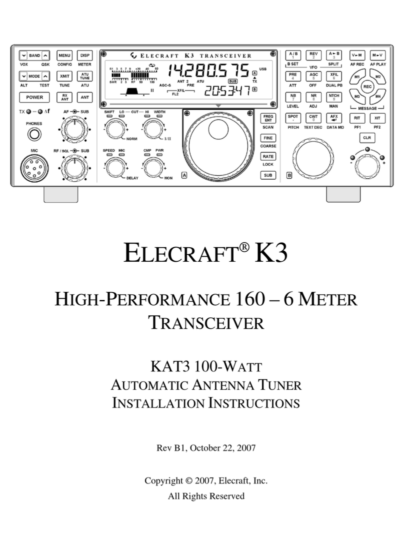
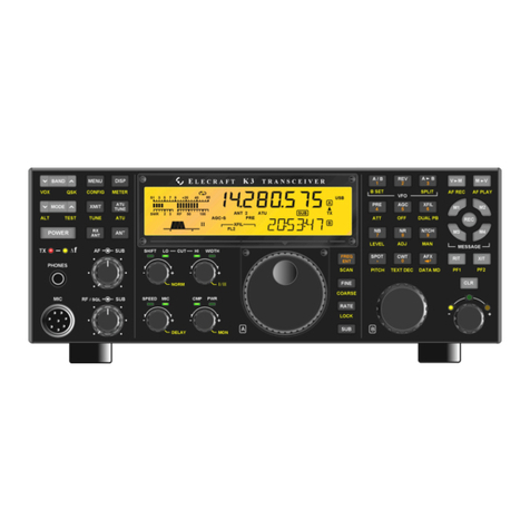
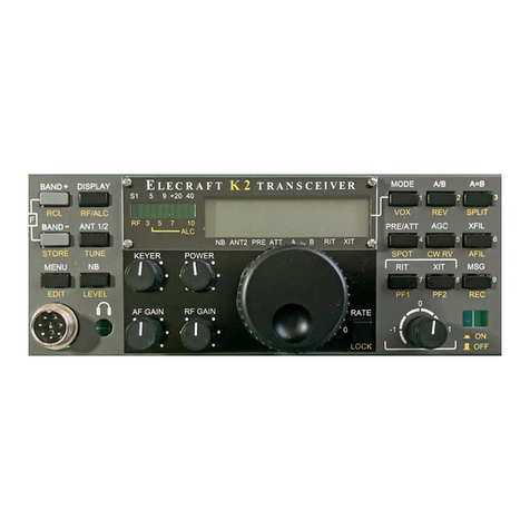
ELECRAFT K2 User manual

ELECRAFT K2
160-10 Meter
SSB/CW
Transceiver
Owner’s Manual
Revision XC, Jan. 25, 1999
Copyright 1999 Elecraft
All Rights Reserved
This revision of the K2 Owner’s Manual is for use by Field
Test participants only. Missing or inaccurate information
will be corrected in the next revision.

K2 Manual 1/24/99 V.XC ©1999 Elecraft 2
Table of Contents
1. INTRODUCTION .............................................................................................................................................................................. 4
2. SPECIFICATIONS............................................................................................................................................................................ 4
3. PREPARATION FOR ASSEMBLY................................................................................................................................................... 7
4. CONTROL BOARD........................................................................................................................................................................ 13
5. FRONT PANEL BOARD ................................................................................................................................................................ 22
6. RF BOARD..................................................................................................................................................................................... 34
7. FINAL ASSEMBLY......................................................................................................................................................................... 78
8. OPERATION .................................................................................................................................................................................. 81
9. MODIFICATIONS ......................................................................................................................................................................... 110
10. THEORY OF OPERATION .......................................................................................................................................................... 111
11. TROUBLESHOOTING................................................................................................................................................................. 119
12. INTERNAL OPTIONS .................................................................................................................................................................. 126
PARTS LIST.........................................................................................................................................................................APPENDIX A
SCHEMATIC.........................................................................................................................................................................APPENDIX B
BLOCK DIAGRAM................................................................................................................................................................APPENDIX C
PHOTOGRAPHS ..................................................................................................................................................................APPENDIX D

K2 Manual 1/24/99 V.XC ©1999 Elecraft 3

K2 Manual 1/24/99 V.XC ©1999 Elecraft 4
1. Introduction
The Elecraft K2 is a high-performance, synthesized transceiver that
provides CW and SSB operation on 160-10 meters. It is a true dual-
purpose transceiver, combining the operating features you’d expect in
a home-station rig with the small size and weight of a rugged, go-
anywhere portable. The K2 is also the first transceiver to offer these
features in kit form.
The basic K2 operates on 80-10 meter CW, with adjustable power
output of over 10 watts. You can also customize your K2 by choosing
from a wide range of internal option kits. These include:
§SSB adapter
§noise blanker
§160 meter adapter + receive antenna switch
§20W automatic antenna tuner
§internal rechargeable battery
§host computer interface
For those who prefer a higher-power station, we’ll be adding an
internal 100W power amplifier kit in the near future1. Other future
options include an internal 6m transverter, high-performance audio
filter, and a variety of matching station accessories.
The K2 is an intermediate-to-advanced kit, yet you’ll be pleasantly
surprised at how uncomplicated it is to build and align. All of the RF
(radio-frequency) circuitry is contained on a single board, while two
plug-in modules provide user interface (UI) and control functions.
1The 100W power amp option displaces the ATU and battery.
Wiring is minimal, unlike traditional kits which depend on complex
wiring harnesses.
A unique feature of the K2 is that it provides its own built-in test
equipment, including a digital voltmeter, ammeter, wattmeter, and
frequency counter. Construction of the kit is sequenced so that these
functions are ready to be used when you begin construction of the RF
board.
In addition to this owner’s manual, you’ll find extensive support for the
K2 on our website, www.elecraft.com. Among the available materials are
manual updates, application notes, photographs, and information on new
Elecraft products. There’s also an Elecraft user forum.
We’d like to thank you for choosing the K2 transceiver, and hope it meets
your expectations for operation both at home and in the field.
Wayne Burdick, N6KR
Eric Swartz, WA6HHQ
Field-Test Acknowledgements
Getting the K2 ready for its field test would not have been possible, or at
least would have taken a lot longer, without the help and encouragement
of Lerma Swartz, Lillian Svec, Bob Dyer, Shigehiro Kinoshita, Conrad
Weiss, and Rob Capon. We’re also grateful for the patience shown by
our field testers.


K2 Manual 1/24/99 V.XC ©1999 Elecraft 4
2. Specifications
All measurements were made with a 13.8V supply and 50 ohm load at
the antenna. Numeric values are typical; your results may be somewhat
different. Specifications are preliminary and subject to change without
notice.
General
Size Cabinet 3.0” H x 7.9” W x 8.3” D
(7.5 x 20 x 21 cm)
Overall 3.4” H x 7.9” W x 9.9” D
(8.5 x 20 x 25 cm)
Weight 3.3 lbs (1.5 kg)
Supply Voltage 8.5 to 15VDC (13.8V nominal);
reverse-polarity protection
Current drain,
Receive100mA in minimum-current
configuration; 150-200mA typical
Transmit21.8A at 10 watts
Frequency control PLL synthesizer w/single VCO
covering 6.7-24 MHz in 9 bands;
fine steps via DAC-tuned VXCO
2Varies with band, supply voltage, configuration, and load impedance.

K2 Manual 1/24/99 V.XC ©1999 Elecraft 5
Frequency range, MHz
Guaranteed 3.5-4.0, 7.0-7.3,
10.0-10.2, 14.0-14.5, 18.0-18.2,
21.0-21.6, 24.8-25.0, 28.0-28.8
Typical [TBD]
160m (opt.)1.8-2.0
VFO Stability [TBD]
Accuracy3+/- 30Hz typ. if calibrated
Resolution 10 Hz
Tuning steps 10 Hz, 50 Hz, and 1000 Hz
Memories 20 (10 general, 10 pre-assigned
to available bands)
Transmitter
Power Output 0.5W to 10W (typ.), all bands;
power setting resolution 0.1W,
power reading accuracy 10% @ 5W
Duty Cycle 5W, 100%
10W, 50%
Spurious products -40dB or better @ 10W (-50typ)
(Transmitter, continued)
Harmonic content -45dB or better @ 10W (-55typ)
3See Frequency Calibration Techniques (Operation section, under Advanced
Operating Features).
Load Tolerance 2:1 or better SWR recommended;
will survive occasional operation
into high SWR
T-R delay 10ms-1.5sec, adjustable
Receiver Preamp On Preamp Off
Sensitivity (MDS) -135dBm -130dBm
3rd-order Intercept 0 to +7.54+14
2nd-order Intercept +77 +78
Dynamic Range,
Blocking 125dB 133dB
Two-tone 96 97
I.F. 4.915 MHz (single conversion)
Selectivity,
CW 5-pole variable-bandwidth crystal
filter, 200-1500 Hz
SSB [TBD]
RIT/XIT Range: +/- 1.2 kHz, 10 Hz steps
Audio output: 1 watt (typ) into 4 ohm load
4Varies with band.

K2 Manual 1/24/99 V.XC ©1999 Elecraft 6
Keyer
Keying modes Iambic A and B
Speed Range Approx. 9 - 40 WPM
Messages 3 buffers, 84 bytes each,
nonvolatile; auto-repeat

K2 Manual 1/24/99 V.XC ©1999 Elecraft 7
3. Preparation for Assembly
Overview of the Kit
The K2 is a highly modular transceiver, both physically and
electrically. This concept extends to the chassis, as can be seen from
Figure 3-1. Any chassis element can be removed to facilitate assembly
or troubleshooting. (Also see photos in Appendix D.)
Top Cover
Front
Panel
Side
Panel
Bottom
Cover
Heat
Sink
(Right side panel
not shown)
Figure 3-1
As shown in Figure 3-2, there are three printed circuit boards (PCBs) in
the basic K2 kit: the Front Panel board, Control Board, and RF board.
The Front Panel and Control boards plug into the RF board directly to
eliminate point-to-point wiring. Gold-plated contacts are used on these
connectors for reliability and corrosion resistance.
RF
Front
Panel
Control
Figure 3-2

K2 Manual 1/24/99 V.XC ©1999 Elecraft 8
There are six steps in the K2 assembly process:
1. Control Board assembly
2. Front Panel Board assembly
3. RF Board assembly and test, part I (control circuits)
4. RF Board assembly and test, part II (receiver and synthesizer)
5. RF Board assembly and test, part III (transmitter)
6. Final assembly
This assembly sequence is important because later steps build on the
previous ones. For example, in step 3 you’ll put the modules together
for the first time, allowing you to try out the K2’s built-in frequency
counter. The counter will then be used in step 4 to align and test the
receiver and synthesizer on 40 meters. In step 5 all the pieces will come
together when you complete the transmitter and filters, then align the
K2 on all bands. The last few details—speaker, tilt stand, etc.—will be
wrapped up in step 6.
Many illustrations are provided in the manual to clarify assembly steps.
In addition, you should familiarize yourself with Appendix D, which
provides photographs of the K2 and its three circuit boards in various
stages of assembly.
Note to Field Testers
During field testing of the K2, you will no doubt discover minor
problems with the kit's documentation, components, etc. Please contact
us if you find something that we've missed. We will suggest corrective
measures as quickly as possible, and we'll ship you any parts needed.
The next revision of the manual will include a number of additional
illustrations and photos. The Theory of Operation and Troubleshooting
sections will also be much more extensive, and we’ll add much more
information for beginning builders and operators (including a glossary
of terms). Revised manual sections will be posted to our website in
downloadable form.
Unpacking
Note: Do not open any of the component bags until instructed to do so.
Small components can easily be lost or confused with similar parts if
you unpack the entire kit at once.
When you open the kit you should find the following items:
§six chassis pieces, wrapped (Figure 3-1)
§three printed circuit boards (Figure 3-2)
§FRONT PANEL board components bag, which includes the LCD
and its backlight assembly in individual small bags
§CONTROL board components bag
§RF board components bag
§MISCELLANEOUS components bag
§4 ohm Speaker
§tube of DPDT latching relays
§Enamel and hookup wire
If any of the above items is missing or damaged, contact Elecraft.
Your kit has been carefully packed, so it is unlikely that any
components are missing. However, if you prefer to do an inventory of
parts, you may do so at any major stage in the assembly process using
the complete parts list in Appendix A. The parts list includes
photographs or illustrations of each type of component. Even if you
don’t do an inventory, it is helpful to familiarize yourself with the parts
list in case you need to refer to it later.

K2 Manual 1/24/99 V.XC ©1999 Elecraft 9
Tools
The following specialized tools are supplied with the K2:
§.050” (1.3mm) Allen Wrench, short handle
§5/64” (2mm) Allen Wrench, long handle
§Double-ended plastic inductor alignment tool
In addition to the tools listed above, you will need these standard tools:
§Fine-tip soldering iron, 15-25 watt (or a temperature-controlled
soldering station)
§IC-grade, small-diameter solder (DO NOT use acid-core solder or
any type of flux)
§Desoldering tools (wick, solder-sucker, etc.)
§Needle-nose pliers
§Small diagonal cutters
§Small phillips screwdriver
§Very small flat-blade screwdriver (for 2-56 bezel screws and
trimmer capacitors)
While not required, the following items are recommended:
§DMM (digital multimeter) for doing resistance and voltage checks.
Even an inexpensive DMM can provide a number of useful
capabilities, including diode and capacitance measurement.
§Illuminated magnifying glass
§Anti-static work surface and wrist strap (see Integrated Circuits
and ESD, below, for more details)
Assembly Notes
i
This symbol is used to alert you to important information about
assembly, alignment, or operation of the K2. You should read and
understand this information before proceeding.
Step-by-Step Assembly
Each step in the K2 assembly process is accompanied by a check-box.
As you complete each step, put a mark in the box:
In some steps you will actually be installing multiple components of a
particular type. In this case the instructions will be followed by a table
listing all of the components to be installed, so you won’t need to refer
to the parts list during assembly. The order that the components are
installed corresponds closely to their locations on the PC board.
Assembly generally begins with low-profile components such as
resistors and diodes, then works up to the higher-profile parts. This
keeps the board stable as you turn it over each time to solder. Do not
skip any steps; you may find that you’ve installed one component that
hinders the installation of another.
Top and Bottom Components
A number of components in the K2 are mounted on the bottom of the
PC boards to improve component spacing or for electrical reasons.
Component outline symbols are provided on both sides of each board,
so it will always be clear which side a particular component goes on.
You’ll be able to tell the top of the board from the bottom easily: the
top side has far more parts.

K2 Manual 1/24/99 V.XC ©1999 Elecraft 10
Components which are mounted on the bottom of a board are identified
on the schematic with this symbol:
Identifying Capacitors
Small (< 1000 pF) fixed capacitors are usually marked with one, two,
or three digits and no decimal point. If one or two digits are used, that is
the value in pF (picofarads). If there are three digits, the third digit is
usually a multiplier. For example, a capacitor marked “151” would be
150pF (15 with a multiplier of 101). Similarly, “330” would be 33 pF,
and “102” would be 1000 pF (or .001µF).
Occasionally, capacitor manufacturers use "0" as a decimal place
holder rather than a multiplier, so that “330” might actually mean 330
pF, not 33 pF. Markings shown in the parts list should clear up any
confusion. If in doubt, you may wish to measure the capacitor using a
DMM.
Fixed capacitors with values over 1000pF may use a decimal point in
the value, such as .001 or .02. This is the value in microfarads (µF).
Capacitors also may have a suffix after the value, such as “.001J.”
You won’t need to use suffixes in identifying capacitors.
Color Code
All resistor and RF choke color bands are provided in the text along
with their values. However, it is helpful to familiarize yourself with the
color code to allow you to identify these components without having to
refer to the text or parts list.
The color-code chart, Figure 3-3, shows how to read the four color
bands on 5% resistors. 1% resistors are similar, except that they use
five bands (three significant digits, multiplier, and tolerance). For
example, a 1,500 ohm (1.5k) 5% resistor has color bands BROWN,
GREEN, and RED. A 1.5k, 1% resistor has color bands BROWN,
GREEN, BLACK, BROWN. The multiplier value is 1 rather than 2 in
the 1% case because of the third significant digit.
The markings on RF chokes reflect their value in microhenries (µH).
Like 5% resistors, chokes use two significant digits and a multiplier.
Example: an RF choke with color bands RED, VIOLET, BLACK
would have a value of 27µH.

K2 Manual 1/24/99 V.XC ©1999 Elecraft 11
Tolerance
(gold = 5%)
Multiplier
Second Digit
First Digit
Color MultiplierDigit
Black 0x 1
Brown 1x 10
Red 2
3x 100
Orange x 1K
Yellow 4x 10K
Green 5x 100K
Blue 6x 1M
Violet 7
Gray 8
White 9
Resistor Color Code
Figure 3-1

K2 Manual 1/24/99 V.XC ©1999 Elecraft 12
Integrated Circuits and ESD
The K2 transceiver uses integrated circuits and transistors that can be
damaged by electrostatic discharge (ESD). Problems caused by ESD
can often be difficult to troubleshoot because components may only be
degraded rather than fail completely. To avoid such problems, we
recommend that you take the following anti-static precautions:
§Remove carpets in your workbench area, or treat them with
antistatic spray
§If you use a rubber floor mat to guard against electric shock, make
sure it is of the anti-static type; any other type of rubber mat will
increase ESD problems
§Wear cotton clothing, not polyester or other synthetics
§Leave all ESD-sensitive components in their anti-static packaging
until you actually install them
§Ground yourself using a wrist strap with a series 1megohm resistor
(do NOT ground yourself directly--this poses a shock hazard)
§Use an anti-static mat
§Use a grounded soldering iron. When soldering ICs and transistors,
you should also keep the chassis and PC boards grounded using
jumper clips. Grounding to the soldering iron's temperature control
box is acceptable.
Sockets are used for only a few of the ICs, including the
microprocessor and display driver. You should not use sockets for the
other ICs, because they tend to be unreliable and can cause problems in
some circuits due to the added lead length.
Since sockets are not used in most cases, you must carefully verify the
type and orientation of each IC before soldering. IC removal and re-
installation is to be avoided since damage to the IC or the PC board
may occur.

K2 Manual 1/24/99 V.XC ©1999 Elecraft 13
4. Control Board
The control board is the “brain” of the K2. It monitors all signals
during receive and transmit, and handles display and control functions
via the front panel board. The microprocessor, analog and digital
control circuits, automatic gain control (AGC), and audio amplifier are
located on this board.
Components
iReview the precautions described in the previous section
before handling any IC’s or transistors. These components can be
damaged by static discharge, and the resulting problems are often
difficult to troubleshoot.
Open the bag of components labeled CONTROL and sort the
parts into groups (resistors, diodes, capacitors, etc.). If any of the
components are unfamiliar, identify them using the illustrations in the
parts list, Appendix A. Doing a components inventory is optional.
Locate the control board. It is the smallest of the three K2 PC
boards, labeled “K2 CONTROL” on the front side, in the lower right-
hand corner. The lower left-hand corner is notched.
Open the bag labeled MISCELLANEOUS and empty the
contents into a small, shallow box or pan. This will prevent loss of any
of the small hardware, while still allowing you to locate items as
needed.
i
The Allen wrenches are located in a small bag with the
MISCELLANEOUS items. These wrenches may have been oiled
during manufacturing. Remove the wrenches and wipe off the oil, if
any, then discard the bag.
Field Test Notes: Two different sizes of small crimp pins were
inadvertently purchased for the field test kits. Two of the pins are for
the speaker connector, and the other three--which are different--are for
the test probes (counter and voltmeter). The test probe crimp pins (3)
and housings (2) are bagged separately and labeled PROBES.
iThere are four sizes of black-anodized, 4-40 machine screws
provided with the kit. The relative sizes of the screws are shown below
for identification purposes (not to scale). The 3/16” (4.8mm) pan-head
screws are the most numerous, and will be referred to as chassis screws
throughout the manual. There is only one Flat-head 3/16” (4.8mm)
screw in the kit.

K2 Manual 1/24/99 V.XC ©1999 Elecraft 14
Flat-head, 3/16” (4.8mm)
Pan-head, 3/16” (4.8mm)
(chassis screws)
Pan-head, 3/8” (9.5mm)
Pan-head, 1/2” (12.7mm)
Assembly
All of the components to be installed are on the top (component side) of
the control board. On the bottom of the board there is an outline for the
audio filter board and its two connectors (J1 and J2), but these items
are not part of the basic K2 kit.
With the top side of the PC board facing you (notch at the lower
left), locate the position of resistor R1, near the upper-left corner. The
label “R1” appears just below the resistor’s outline.
Install a 100k resistor (brown-black-yellow) at R1, with its first
color band (brown) at the top. Make sure it is seated flush with the
board, then bend the leads on the bottom to hold it in place. Do not
solder this resistor until the remaining fixed resistors have been installed
in the next step.
Install the remaining fixed resistors, which are listed below in left-
to-right PC board order. The resistors should all be oriented with the
first significant-digit band towards the left or top. This will make the
color codes easier to read if you need to re-check the values after
installation.
Note: When multiple items appear on one line in a component list such
as the one below, complete all items on one line before moving on to the
next, as indicated by the small arrow. (In other words, install R5 first,
then R2, then go to the second line.)
__ R5, 33k (ORG-ORG-ORG) ⇒__ R2, 3.3M (ORG-ORG-GRN)
__ R3, 33k (ORG-ORG-ORG) __ R6, 470 (YEL-VIO-BRN)
__ R7, 1.96K, 1% (BRN-WHT-BLU-BRN)
__ R8, 100, 1% (BRN-BLK-BLK-BLK)
__ R9, 806K, 1% (GRY-BLK-BLU-ORG)
__ R10, 196K, 1% (BRN-WHT-BLU-ORG)
__ R16, 10 (BRN-BLK-BLK) ⇒__ R17, 10M (BRN-BLK-BLU)
__ R19, 1.5k (BRN-GRN-RED) __ R18, 1.5k (BRN-GRN-RED)
__ R21, 10k (BRN-BLK-ORG) __ R20, 2.7ohms (RED-VIO-GLD)
Solder all of the resistors, then trim the leads as close as possible to
the solder joints. (If the leads get in the way during soldering, try
soldering and trimming a few leads at a time.)
Locate RP6, a 10K, 10-pin resistor network (labeled
“10A3.103G”). (“RP” means “resistor pack,” another name for resistor
networks.) Note that one end of the resistor network has a dot,
indicating pin 1.
Locate the component outline for RP6 at the left end of the PC
board. Install the resistor network so that the end with the dot is lined
up with the “1” label.
Make sure the resistor network is seated firmly on the board, then
bend the leads at the far ends in opposite directions to hold it in place.
(It is not necessary to clip the leads.) Do not solder RP6 yet.

K2 Manual 1/24/99 V.XC ©1999 Elecraft 15
iResistor networks and other components with many leads are
difficult to remove once soldered. Double-check the part numbers and
orientation before soldering.
Install the remaining resistor networks in the order listed below.
Do not solder them until the next step.
__ RP1, 3.9k, 10 pins (10A3.392G)
__ RP7, 33k, 8 pins (8A3.333G)
__ RP2, 82k, 8 pins (77083823)
__ RP3, 47k, 10 pins (10A3.473G)
__ RP5, 470, 10 pins (10A3.471G)
__ RP4, 82k, 8 pins (77083823)
Solder all of the resistor networks.

K2 Manual 1/24/99 V.XC ©1999 Elecraft 16
Install the diodes listed below, beginning with D1, which is in the
upper left-hand corner of the PC board. (Refer to the parts list if
necessary to identify the different types of diodes.) If a diode has only
one band, the end with the band (the cathode) should be oriented
towards the banded end of the corresponding PC board outline. If a
diode has multiple bands, the widest band indicates the cathode end.
__ D1, 1N4148 __ D2, 1N4148 __ D3, 1N5817
Double-check the orientation of the diodes, then solder.
Install the small fixed capacitors listed below, beginning with C2
in the upper left-hand corner of the board. (This list includes all of the
fixed capacitors on the control board except the tall, cylindrical
electrolytic types, which will be installed later.) The list shows both the
value and the capacitor labels, using notation explained in the previous
section. After installing each capacitor, bend and clip the leads, but do
not solder until the next step.
Note: Remember to complete all items in each line before moving on to
the next. (Install C2, C3, and C4, then C7, etc.)
__ C2, .001 (102) ⇒__ C3, .01 (103) ⇒__ C4, 0.47 (474)
__ C7, 330 (331) __ C6, .047 (473) __ C8, 39 (39)
__ C9, .01 (103) __ C10, .01 (103) __ C12, .001 (102)
__ C5, .01 (103) __ C14, .047 (473) __ C17, .01 (103)
__ C11, .01 (103) __ C16, .047 (473) __ C18, .01 (103)
__ C19, .047 (473) __ C21, 33 (33) __ C20, .001 (102)
__ C23, .01 (103) __ C27, .022 (223) __ C25, 0.1 (104)
__ C26, 0.1 (104) __ C24, .0027 (272) __ C31, 0.1 (104)
__ C34, .001 (102) __ C30, .047 (473) __ C40, .01 (103)
__ C35, .01 (103) __ C36, .0027 (272) __ C39, .01 (103)
__ C41, .01 (103) __ C37, .01 (103) __ C38, 680 (681)
Solder all of the small fixed capacitors.
Install and solder the electrolytic capacitors listed below, which
are polarized. Be sure that the (+) lead is installed in the hole marked
with a “+” symbol. The (+) lead is usually longer than the (–) lead, and
the (–) lead is identified by a black stripe (Figure 4-1).
+
-
Figure 4-1
__ C1, 2.2µF ⇒__ C13, 22µF ⇒__ C15, 100µF
__ C28, 220µF __ C29, 220µF __ C33, 2.2µF
__ C32, 22µF
Install and solder ceramic trimmer capacitor C22. Orient the flat
side of this trimmer as shown on its PC board outline. Be sure that the
capacitor is seated flush with the PC board, then solder.
Using a small flat-blade screwdriver, set C22 to the mid-point in
its rotation. The screwdriver slot should be parallel to the outline of
crystal X2, just above C22 on the PC board.
iThe trimmer you just installed, C22, is used to calibrate the
master 4.000 MHz crystal oscillator, which determines the accuracy of
the built-in frequency counter and VFO. The standard setting given
above will suffice in most cases, but if you wish to more accurately
calibrate C22, refer to the Operation section under Advanced Operating
Features.
Locate Q12 (type PN2222A), which is a small, black TO-92
package transistor. Note: Q12 and other TO-92 transistors may have
either of the two shapes shown in Figure 4-2. In all cases the flat side of
the device should be aligned with the flat side of the component outline.

K2 Manual 1/24/99 V.XC ©1999 Elecraft 17
Figure 4-2
Install Q12 near the upper left-hand corner of the PC board. Align
the flat side of Q12 with its PC board outline as in Figure 4-2. The
body of the transistor should be about 1/8” (3mm) above the board;
don’t force it down too far or you may break the leads. Bend the leads
of the transistor outward slightly on the bottom to hold it in place.
Solder Q12.
Install the remaining TO-92 package transistors in the order listed
below.
__ Q12, PN2222A __ Q11, PN2222A __ Q1, 2N3906
__ Q2, 2N3906 __ Q3, 2N7000 __ Q4, 2N7000
__ Q5, 2N7000 __ Q6, J310 __ Q7, J310
__ Q8, PN2222A __ Q9, MPS5179__ Q10, MPS5179
Solder all of the above transistors.
iWhen installing crystals, you must use the thin spacers
provided in the MISCELLANEOUS bag to keep the crystal cans from
shorting to their pads on the top of the board. The need for these spaces
will be eliminated with the next revision of the PC board by using the
solder mask to cover the pads on the top of the board.
Slip a crystal spacer over the leads of each crystal (X1 and X2).
Install crystals X1 and X2 so that they are flat against the board.
X1 is 5.068 MHz and is located near the notch in the lower left-hand
corner. X2 is 4.000 MHz, and is located near the center of the board.
Solder the crystals.
The cases of the crystals should be grounded to minimize signal
radiation (Figure 4-3). Insert a 1” (25mm) length of bare, solid hookup
wire into the provided grounding hole and solder it on the bottom of the
board. Then fold the bare wire over the crystal and solder it to the top
of the can. (Don’t overheat the crystals or cover the entire top surface
of the crystal with solder; only a small amount of solder is required.)
X1 X2
Figure 4-3
i
The voltage regulators, U4 and U5, will be installed in the
following steps. These regulators have different output voltages and
must not be interchanged. Check the labels on the regulators carefully
before soldering; the basic part numbers should match those on the PC
board outline.

K2 Manual 1/24/99 V.XC ©1999 Elecraft 18
Install U4 (LM2930T-8) and U5 (LM7805), bending the leads as
indicated (Figure 4-4). Long-nosed pliers should be used because the
indicated bend location may be at the thicker part of the lead. After
inserting the leads into the proper holes, secure each IC with a 4-40 x
3/8” (9.5mm) machine, #4 lockwasher, and 4-40 nut. (Note: these
regulators may have either plastic or metal mounting tabs.)
Bend pins
down 90°
Figure 4-4
Solder the voltage regulator ICs.
Install a 40-pin IC socket at U6. (The microprocessor will be
inserted into the socket in a later step.) Orient the notched end of the
socket to the left as shown on the PC board outline. Bend two of the
socket’s corner leads slightly to hold the socket in place, then solder
only these two pins. If the socket does not appear to be seated flat on
the PC board, reheat the solder joints one at a time while pressing on
the socket.
Solder the remaining pins of the 40-pin socket.
i
The connectors used in the following steps have plastic bodies
that can may melt if too much heat is applied during soldering, causing
the pins to be mis-positioned. Limit soldering time for each pin to 3
seconds maximum (1 to 2 seconds should be adequate).
Install the 2-pin male connectors, P5 and P6. As shown in Figure
4-5, the short end of the connector pins are inserted into the PC board.
P5, the voltmeter input connector, can be found near the upper left-hand
corner of the board. P6 is used for frequency counter input, which is in
the upper right-hand corner.
2-pin
connector
Top side of
PC Board
Figure 4-5
Install the 10-pin, dual-row connector, P4. It is located to the left
of P5. It must be seated flat on the board before soldering.
Install S1, the miniature slide switch, to the right of P5.
At the upper left and right corners of the board you’ll find two
short jumpers, each labeled with a ground symbol ( ). These jumpers
are provided for connecting clip leads during alignment and test. Form a
3/4 (19mm) length of bare copper hookup wire into a “U” shape for
each jumper (Figure 4-6). (You can use a clipped component lead as an
alternative to hookup wire.) Solder the jumpers on the bottom of the
board.
Figure 4-6
Other manuals for K2
7
Table of contents
Other ELECRAFT Transceiver manuals

ELECRAFT
ELECRAFT K3 User manual

ELECRAFT
ELECRAFT K3S KAT3A User manual

ELECRAFT
ELECRAFT K2 Operating instructions

ELECRAFT
ELECRAFT K3S Instruction Manual

ELECRAFT
ELECRAFT K3 User manual

ELECRAFT
ELECRAFT K3 Quick start guide

ELECRAFT
ELECRAFT K2 Reference guide

ELECRAFT
ELECRAFT K3 User manual

ELECRAFT
ELECRAFT K1 User manual

ELECRAFT
ELECRAFT KX3-2M Supplement

ELECRAFT
ELECRAFT KRX3 Owner's manual

ELECRAFT
ELECRAFT KX2 User manual

ELECRAFT
ELECRAFT KX3 User manual

ELECRAFT
ELECRAFT K4 User manual

ELECRAFT
ELECRAFT P3 User manual

ELECRAFT
ELECRAFT K3S User manual

ELECRAFT
ELECRAFT K2/100 User manual

ELECRAFT
ELECRAFT K3 User manual

ELECRAFT
ELECRAFT K2 User manual

ELECRAFT
ELECRAFT K4 User manual