Endace DAG 7.1S User manual

DAG 7.1S Card
User Guide
EDM01-17

EDM 01-17 DAG 7.1S Card User Guide
Published by:
Endace Limited
Building 7
Lambie Drive
PO Box 76802
Manukau City 1702
New Zealand
Phone: +64 9 262 7260
Fax: +64 9 262 7261
EDM01.06-17
p
re1
www.endace.com
International Locations
New Zealand
Endace Technology® Ltd
Level 9
85 Alexandra Street
PO Box 19246
Hamilton 2001
New Zealand
Phone: +64 7 839 0540
Fax: +64 7 839 0543
Americas
Endace USA® Ltd
Suite 220
11495 Sunset Hill Road
Reston
Virginia 20190
United States of America
Phone: ++1 703 382 0155
Fax: ++1 703 382 0155
Europe, Middle East & Africa
Endace Europe® Ltd
Sheraton House
Castle Park
Cambridge CB3 0AX
United Kingdom
Phone: ++44 1223 370 176
Fax: ++44 1223 370 040
Copyright 2005-2006© Endace Limited. All rights reserved. No part of this publication may be reproduced,
stored in a retrieval system, or transmitted, in any form or by any means electronic, mechanical, photocopying,
recording, or otherwise, without the prior written permission of the publisher.
Version 3: June 2006 ©2005-2006

EDM 01-17 DAG 7.1S Card User Guide
Protection Against Harmful Interference
When present on equipment this manual pertains to, the statement "This device complies with part 15 of the FCC rules"
specifies the equipment has been tested and found to comply with the limits for a Class A digital device, pursuant to Part 15
of the Federal Communications Commission [FCC] Rules.
These limits are designed to provide reasonable protection against harmful interference when the equipment is operated in a
commercial environment.
This equipment generates, uses, and can radiate radio frequency energy and, if not installed and used in accordance with the
instruction manual, may cause harmful interference to radio communications.
Operation of this equipment in a residential area is likely to cause harmful interference in which case the user will be
required to correct the interference at his own expense.
Extra Components and Materials
The product that this manual pertains to may include extra components and materials that are not essential to its basic
operation, but are necessary to ensure compliance to the product standards required by the United States Federal
Communications Commission, and the European EMC Directive. Modification or removal of these components and/or
materials, is liable to cause non compliance to these standards, and in doing so invalidate the user’s right to operate this
equipment in a Class A industrial environment.
Disclaimer
Whilst every effort has been made to ensure accuracy, neither Endace Limited nor any employee of the company, shall be
liable on any ground whatsoever to any party in respect of decisions or actions they may make as a result of using this
information.
Endace Limited has taken great effort to verify the accuracy of this manual, but assumes no responsibility for any technical
inaccuracies or typographical errors.
In accordance with the Endace Limited policy of continuing development, design and specifications are subject to change
without notice.
©2005-2006 Version 3: June 2006


EDM 01-17 DAG 7.1S Card User Guide
Table of Contents
Chapter 1: Introduction 1
Overview 1
Purpose of this User Guide 1
System Requirements 2
Card Description 3
Card Architecture 4
Extended Functions 5
Chapter 2: Installation 7
Introduction 7
DAG Driver Device 7
Inserting the DAG Card 7
Port Connectors 8
Pluggable Optical Transceivers 8
Chapter 3: Configuring the Card 11
Introduction 11
Line Characteristics 11
LEDs and Inputs 12
Receiver Port Signal Levels 12
Specific Network Configuration 13
Chapter 4: Concatenated Configuration 15
Load the FPGA Images 15
Available Configurations 15
Display Current Configuration 15
Verify Optical Signal 17
Verify Mapping/ Framing Setup 18
ATM Mode 19
PoS Mode 20
Interface Statistics 21
Status Conditions 23
Verify Configuration 24
Chapter 5: Channelised Configuration 25
Load the FPGA Images 25
Available Configurations 25
Display Current Configuration 25
Verify Optical Signal 27
Verify Mapping/ Framing Setup 28
Configure Line Type 29
Interface Statistics 30
E1 OC-12 30
T1 OC-12 31
Interface Statistics (cont. 32
Status Conditions 32
Verify Configuration 33
Configuring Channels 34
Valid Configurations 34
Supported Channel Types 36
Configuration File 36
©2005-2006 i Version 3: June 2006

EDM 01-17 DAG 7.1S Card User Guide
Chapter 6: Capturing Data 39
Starting a Session 39
Setting Captured Packet Size 39
Snaplength 39
Variable/Fixed Length 40
Enabling/ Disabling Ports 40
High Load Performance 41
Overview 41
Avoiding Packet Loss 41
Detecting Packet Losses 41
Increasing Buffer Size 42
Transmitting 42
Configuration 42
Explicit Packet Transmission 43
Trace Files 43
Configuring Extended Functions 44
Overview 44
Loading the Images 44
Starting the IXP 45
Directing Data to the IXP 45
Using the AAL Reassembler 45
Using the PoS IP Filter 46
Chapter 7: Synchronizing Clock Time 47
Overview 47
DUCK Configuration 47
Common Synchronization 47
Timestamps 48
Configuration Tools 49
Card with Reference 50
Overview 50
Pulse Signal from External Source 50
Connecting the Time Distribution Server 50
Testing the Signal 50
Single Card No Reference 51
Two Cards No Reference 51
Synchronising with Each Other 52
Synchronising with Host 52
Connector Pin-outs 53
Chapter 8: Data Formats 55
Overview 55
Generic Header 55
Type-1 Record 57
Type-3 Record 57
Type-4 Record 57
Type-5 Record 58
Type-7 Record 59
Type 9 Record 60
Type 12 Record 61
Type 18 Record 62
Chapter 9 Troubleshooting 63
Reporting Problems 63
Version 3: June 2006 ii ©2005-2006

EDM 01-17 DAG 7.1S Card User Guide
Chapter 1:
Introduction
Overview The Endace DAG 7.1S card provides the means to transfer data at the full
speed of the network into the memory of the host PC, with zero packet loss
guaranteed in even worst-case conditions. Further, unlike a NIC, Endace
products actively manage the movement of network data into memory
without consuming any of the host PC's resources. The full attention of the
CPU remains focused on the analysis of incoming data without a constant
stream of interruptions as new packets arrive from the network. For a busy
network link, this feature has a turbo-charging effect similar to that of adding
a second CPU to the system.
The DAG 7.1S is a network monitoring interface card specifically designed
to provide high efficiency monitoring and transmission of ATM, POS or Bit
HDLC traffic with precision timestamping capability.
It supports the following:
•Concatenated POS/ATM receive and transmit over 4 x OC-3c/STM-1c or
4 x OC-12c/STM-4c.
•Channelised Bit HDLC/ATM receive and transmit over 4 x OC-3/STM-1
or 2 x OC-12/STM-4.
Purpose of
this User
Guide
Description
The purpose of this User Guide is to provide you with an understanding of
the DAG card architecture and functionality and to guide you through the
following:
•Installing the card and associated software and firmware,
•Configuring the card for your specific network requirements,
•Running a data capture session,
•Synchronising clock time,
•Data formats
You can also find additional information relating to functions and features of
the DAG 7.1S card in the following documents which are available from the
Support section of the Endace website at www.endace.com:
•EDM04-08 Configuration and Status API Programming Guide
•EDM04-13 SAR API Programming Guide
•EDM04-11 IXP Filter API Programming Guide
•EDM04-08 DAG IXP Filter Loader User Guide
This User Guide and the Linux and Window Guides are also available in PDF
format on the Installation CD shipped with your DAG 7.1S card.
©2005-2006 1 Version 3: June 2006

EDM 01-17 DAG 7.1S Card User Guide
System
Requirements General
The minimum system requirements for the DAG 7.1S card are :
•PC, at least Intel Xeon 1.8GHz or faster
•Minimum of 256 MB RAM
•At least one free PCI-Express slot supporting at least one lane
•Software distribution requires 30MB free space
•6GB for installation of Endace software, which is optional
Operating System
This User Guide assumes you are installing the DAG card in a PC which
already has an operating system installed.
However for convenience, a copy of Debian Linux 3.1 (Sarge) is provided as
a bootable ISO image on the CDs that is shipped with the DAG card.
To install either the Linux/FreeBSD or Windows operating system please
refer to the following documents which are also included on the CD that is
shipped with the DAG card.
•EDM04-01 Linux FreeBSD Software Installation Guide
•EDM 04-02 Windows Software Installation Guide
Other Systems
For advice on using an operating system that is substantially different from
either of those specified above, please contact Endace Customer Support at
Version 3: June 2006 2 ©2005-2006

EDM 01-17 DAG 7.1S Card User Guide
Card
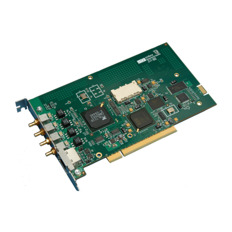
Description The DAG 7.1S SDH/SONET Network Monitoring Card provides either four
STM-1 (OC3) or two STM-2 (OC12) interfaces supporting concatenated or
channelised ATM or Packet Over Sonet (POS) networks.
The DAG 7.1S has four optical transceivers which can be operated
simultaneously.
The key features of the card are:
•Four interfaces allow full line rate capture and processing for
4 x STM-1/OC-3 or 2 x STM-2/OC-12.
•Fully programmable Intel IXP Network Processor
•PCI Express bus interface.
•1244Mpps raw transmit and receive bandwidth.
•Combined FPGA and network processor architecture.
•Channelised and concatenated support.
•ATM AAL2 and AAL5 segmentation and reassembly.
•PoS IP filtering
Extra Power Connecto
r
FPGAs
Optical Transceiver
s
IXP2350 Network Processo
r
RJ45 Connector
©2005-2006 3 Version 3: June 2006

EDM 01-17 DAG 7.1S Card User Guide
Card
Architecture Serial SONET/SDH optical data is received by four optical interfaces, and
passed through deserializers.
The network data feeds immediately into two physical layer FPGAs. The
SONET/SDH payload data is then sent to the main FPGA.
The FPGA contains the packet record processor, PCI Express interface
logic and the DAG Universal Clock Kit (DUCK) timestamp engine. The
DUCK provides high resolution per packet timestamps which can be
accurately synchronised..
Note: For further information on the DUCK and time synchronising
please refer to Chapter 7: Synchronising Clock Time later in this
User Guide.
An Intel IXP network processor is logically located next to the main
FPGA. The main FPGA can route packets to either the IXP network
processor for additional processing before routing onto the host or directly
to the host via the PCI-Express port.
The following diagram shows the card’s major components and the flow
of data.
Version 3: June 2006 4 ©2005-2006

EDM 01-17 DAG 7.1S Card User Guide
Extended
Functions In addition to standard packet capture the DAG 7.1S card also provides
TCP/IP Filtering and Classification and ATM Segmentation and
Reassembly
TCP/IP Filtering and Classification
This feature allows you to classify packets into arbitrary categories which
then drop, retransmit or capture a packet to the host based upon the result.
You can also change filter rules “on the fly” with any loss of data
The specifications for the IP filtering/packet classification are:
•Packets are classified and filtered by IP header (both IPv4 and IPv6)
and/or UDP/TCP/SCTP port number.
•Up to 1024 IP header classification rules.
•Up 254 UDP/TCP/SCTP port or ICMP type rules can set per IP header
classification.
•Classification rules are assigned a user-defined 14-bit identifier
•Packets matching classification rules are assigned the matching rule's
identifier.
•Programmable actions may be associated with each rule identifier. For
example the packet should either be dropped, or presented to the host.
•Packets presented to the host include the rule-match identifier in the
record header.
AAL2/AAL5 Reassembly
This feature allows you to eliminate the significant CPU load associated
with AAL2/AAL5 reassembly on a busy ATM link by offloading this
process to the DAG card. It also provides the ability to reduce volume of
captured data to only what is required by filtering on VPI/VCI pairs.
The Reassembler specifications are:
•Supports up to 8160 simultaneously active VCI/VPI/CIDs
•Supports simultaneous reassembly of AAL2 and AAL5 frames up to
8kB long.
•VPI/VCI scanning
•Supports up to full STM-4/OC-12 cell rate on two interfaces
simultaneously (approx 2.8 million cells/sec), or four full STM-1/OC-3
interfaces for AAL 5 reassembly.
•Supports 2 x STM-1/OC-3 cell rate on combined four interfaces
(approx 0.8 million cells/sec) for AAL2 reassembly.
•Optional ATM cell filtering prior to reassembly.
©2005-2006 5 Version 3: June 2006

EDM 01-17 DAG 7.1S Card User Guide
Version 3: June 2006 6 ©2005-2006

EDM 01-17 DAG 7.1S Card User Guide
Chapter 2:
Installation
Introduction A DAG 7.1S card can be installed in any free PCI-Express slot.
The DAG 7.1S card operates on a single lane PCI-Express, this interface
is capable of providing a maximum throughput of 1.8Gbits/s for both
receive and transmit.
You can run multiple DAG 7.1S cards on one bus. By default, the DAG
driver supports up to four DAG cards in one system.
DAG Driver
Device The DAG device driver must be installed before you install the DAG card
itself.
If you have not already completed this please follow the instructions in
EDM04-01 Linux FreeBSD Software Installation Guide or EDM 04-02
Windows Software Installation Guide as appropriate, which are included on
the CD shipped with the DAG card.
Inserting the
DAG Card To insert the DAG card in the PC follow the steps described below:
•Turn power to the computer OFF,
•Remove the PCI bus slot screw and cover,
•Insert DAG card into PCI-e bus slot ensuring that it is firmly seated in
the slot,
•Check the free end of the card fits securely into the card-end bracket
that supports the weight of the card,
•Secure the card with the bus slot screw,
•Connect the extra power connector located on the top edge of the card.
Note: Ensure you do this before powering up the computer. Failure
to do so may cause damage to the card.
•Turn power to the computer ON.
Extra Power
Connector
©2005-2006 7 Version 3: June 2006

EDM 01-17 DAG 7.1S Card User Guide
Port
Connectors The DAG 7.1S has 4 SFP socket connectors. Each connector consists of an
optical fibre transmitter and receiver.
The upper connector of each pair is used for the transmit signal. These can
be connected to daisy-chain systems if you have facility loopback (fcl) set
on the card. You can also connect them if you are using a data generation
programme.
The bottom connector of each pair is used for the received signal.
There is an 8-pin RJ-45 socket located below the optical port connectors
on the car bracket. This is available for connection to an external time
synchronisation source.
Caution: Never connect an Ethernet network or telephone line to the
RJ-45 sockets.
Pluggable
Optical
Transceivers
Overview
The DAG7.1S card uses industry standard Small Form-factor Pluggable
(SFP) optical transceivers.
The transceivers consists of two parts:
•Mechanical chassis attached to the circuit board
•Transceiver unit which may be inserted into the chassis
Note: You must select the correct transceiver type to match the
optical parameters of the network to which you want t connect.
Configuring the card with the wrong transceiver type may damage
the card.
You can connect the transceiver to the network via LC-style optical
connectors.
For further information on Pluggable Optical Transceiver please refer to
the Endace website at www.endace.com/dagpluggable.htm.
Setting Power
The optical power range depends on the particular SFP module that is
fitted to the DAG card.
However Endace recommends the SFP modules described below which
can be supplied with the DAG 7.1S card:
Manufacturer Part number
Finisar FTRJ1322
Finisar FTRJ1323
TRPD12MM3EAS
Optical Communication Products
Optical Communication Products TRPD03MM3EAS
Version 3: June 2006 8 ©2005-2006

EDM 01-17 DAG 7.1S Card User Guide
Pluggable
Optical
Transceivers
(cont.)
Optical power is measured in dBm. This is decibels relative to 1 mW where
10 dB is equivalent to a factor of 10 in power.
The optical power is always a negative value, indicating power that is less
than 1 mW. The most sensitive devices can work at power levels down as
low as –30dBm or 1µW.
The DAG 7.1S card optical power module configuration for Multi Mode
Fibre (MMF) and Single Mode Fibre (SMF) is shown below:
Part # Fibre Data
Rate Max
Pwr Min
Pwr Nom
Pwr Mode
FTRJ1322 SMF 622 -8dBm -28dBm
- OC-12 Single Mode
FTRJ1323 SMF 155 -8dBm -28dBm
- OC-3 Single Mode
TRPD12MM3EAS MMF 622 - - -
OC-12 Multi Mode
TRPD03MM3EAS MMF - -
155 -
OC-3 Multi Mode
Power Input
Note: The optical power input to the DAG card must be within the
receiver’s dynamic range of 0 to -22dBm. If it is slightly outside of
this range it will cause an increased bit error rate. If it is
significantly outside of this range the system will not be able to
lock onto the SONET signal.
When power is above the upper limit the optical receiver saturates
and fails to function. When power is below the lower limit the bit
error rate increases until the device is unable to obtain lock and
fails. In extreme cases, excess power can damage the receiver.
When you set up the DAG card you should measure the optical power at
the receiver and ensure that it is within the specified power range. If it is
not, adjust the input power as follows:
•Insert an optical attenuator if power is too high, or
•Change the splitter ratio if power is too high or too low.
Splitter Losses
Splitters have the insertion losses either marked on their packaging or
described in their accompanying documentation. General guidelines are:
•A 50:50 splitter will have an insertion loss of between 3 dB and 4 dB
on each output
•90:10 splitter will have losses of about 10 dB in the high loss output,
and <2 dB in the low loss output
Note: A single mode fibre connected to a multi-mode input will have
minimal extra loss. However a multi-mode fibre connected to a
single mode input will create large and unpredictable loss.
©2005-2006 9 Version 3: June 2006

EDM 01-17 DAG 7.1S Card User Guide
Version 3: June 2006 10 ©2005-2006

EDM 01-17 DAG 7.1S Card User Guide
Chapter 3:
Configuring the Card
Introduction Configuring the DAG card for data capture involves the following steps:
•Loading the images and programming the FPGAs,
•Setting the link,
•Checking the link,
•Configuring the connections,
•Capturing data.
The DAG 7.1S card uses four integrated SONET/SDH ATM/PoS physical
layer interface devices to support capture of ATM cells or Bit HDLC and PoS
data frames.
The dagconfig tool which is also supplied with the DAG card allows you to
configure the card to your specific network requirements as well as view
interface statistics. Sample dagconfig outputs are shown later in this
chapter.
Line
Characteristics Overview
It is important that you understand the physical characteristics of the network
to which you want to connect before you begin configuring the card.
Because of its flexibility the card will accept a wide range of settings.
However if they are not the correct settings for your network, the card will
not function as expected.
Note: If you are unsure about which of the options listed below apply
to your network, please contact your Network Administrator for further
information before proceeding with configuring the card.
Supported Line Types
The line characteristics supported by the DAG 7.1S card are described below.
PoS/ATM Packet over SONET/Asynchronous Transfer Mode.
OC-3/OC-3c
A SONET network line with transmission speeds up to
155.52 Mbit/s using fiber optics. Also called STM-1 (SDH).
A SONET network line with transmission speeds up to
622.08 Mbit/s using fiber optics. Also called STM-4 (SDH).
OC-12/OC-12c
An SDH line equivalent to OC-3 (SONET).
STM-1/STM-1c
An SDH line equivalent to OC-12 (SONET).
STM-4/STM-4c
©2005-2006 11 Version 3: June 2006

EDM 01-17 DAG 7.1S Card User Guide
LEDs and
Inputs Before you begin to configure the DAG card it is important to understand the
function of the various LEDs associated with the card, as well as the sockets
on the PCI bracket.
Receiver Port
Signal Levels
PCI Burst Manager:
Should be on when
capture is in progress Port D Port C Port B Port A
PCI FPGA Status:
Should be on after
computer is started
PPS Out: Indicates the card is
receiving an external time
synchronisation signal PPS Out: Indicates the card is sending an
external time synchronisation signal
RJ45 socket for time
synchronisation input
Caution: Ensure that you insert only OC-3/OC-12 modules. Do not use
OC-48 or GiG-E modules as these will destroy the PHY FPGA
The card supports 1310 nanometer singlemode and multimode fibre
attachments with optical signal strength between 0 dBm and -22 dBm.
If there is doubt, check card receiver ports light levels are correct using an
optical power meter.
The card receiver ports are the lower of each dual-LC-style connectors, the
closest to the PCI-Express slot.
Cover card transmit ports with LC-style plugs to prevent dust and mechanical
hazards damaging optics if not in use.
Version 3: June 2006 12 ©2005-2006

EDM 01-17 DAG 7.1S Card User Guide
Note: If you remove the optics modules for any reason they will not
automatically power on when re-inserted. You will need to turn them
on using the sfppwr option when you configure the card channelised or
concatenated operation.
Specific
Network
Configuration
For detailed information on configuring the DAG 7.1S for data capture on
concatenated and channelised networks please refer to Chapter 4:
Concatenated Configuration and Chapter 5: Channelised Configuration.
©2005-2006 13 Version 3: June 2006

EDM 01-17 DAG 7.1S Card User Guide
Version 3: June 2006 14 ©2005-2006
Other manuals for DAG 7.1S
1
Table of contents
Other Endace Computer Hardware manuals
Popular Computer Hardware manuals by other brands
Technologic Systems
Technologic Systems TS-7400 Hardware & software installation
AMX
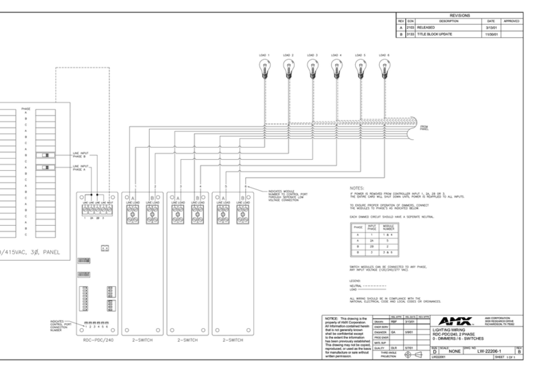
AMX RDC-PDC/240 Schematic diagram
Elenco Electronics
Elenco Electronics K-23 Assembly and instruction manual

A.E.B.
A.E.B. 628450000 Assembly & instruction manual
Keyestudio
Keyestudio ESP32 manual
ST
ST STM8SVLDISCOVERY Application note
Vertiv
Vertiv Liebert CRV Installer/user guide

Ultra Products
Ultra Products ChillTec Thermo Electric Cooler ULT33186 Specifications
EK-Quantum
EK-Quantum Velocity2 D-RGB -LGA 1700 user guide
Texas Instruments
Texas Instruments TPS62065 user guide
Mouser Electronics
Mouser Electronics Si51211 quick start guide

Fireye
Fireye BurnerLogiX ZB110 manual
