1
1.0 INTRODUCTION
The rapid advancement in the electronics industry during the past decade has placed an
increasing importance on the understanding of electrostatics and its effect on electronic
devices and systems. Electrostatic discharge (ESD) is a common cause of microelectronic
circuit failure. Many devices can be seriously damaged or destroyed by an electrostatic
discharge below 20 Volts. The sensitivity to ESD of other components has also become
evident through use, testing and failure analysis. The trend in technology towards greater
complexity, increased packaging density and hence thinner dielectrics between active
elements result in parts becoming even more sensitive to ESD.
Failure mechanisms of electrical and electronic parts due to ESD typically include thermal
breakdown, metalization melt and bulk breakdown that are power dependent; dielectric
breakdown, metalization to metalization arc over, surface breakdown and surface inversion
that are voltage dependent.
ESD can also induce latent failure mechanisms in both MOS structures and bipolar
junctions in both discrete devices and microcircuits. This latent failure mechanism results in
performance degradation and eventually a failure.
Personnel are prime sources of ESD for damaging electrical and electronic parts.
Electrostatic charges generated by rubbing or separating materials are readily transmitted
to a person’s conductive sweat layer charging that person. When a person handles or
comes in close proximity to an ESD sensitive part, that part can then be damaged from a
direct discharge by touching the part or by subjecting the part to an electrostatic field.
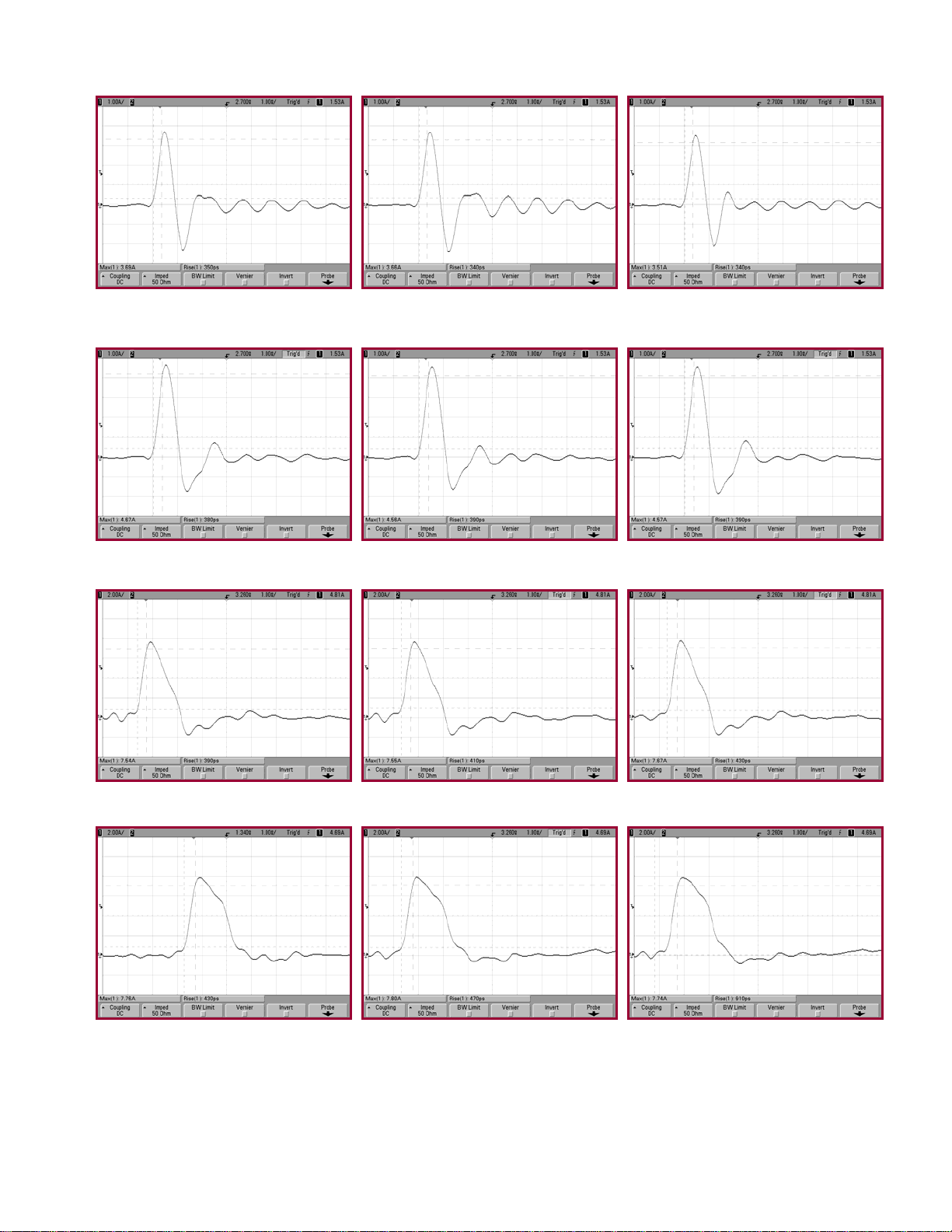
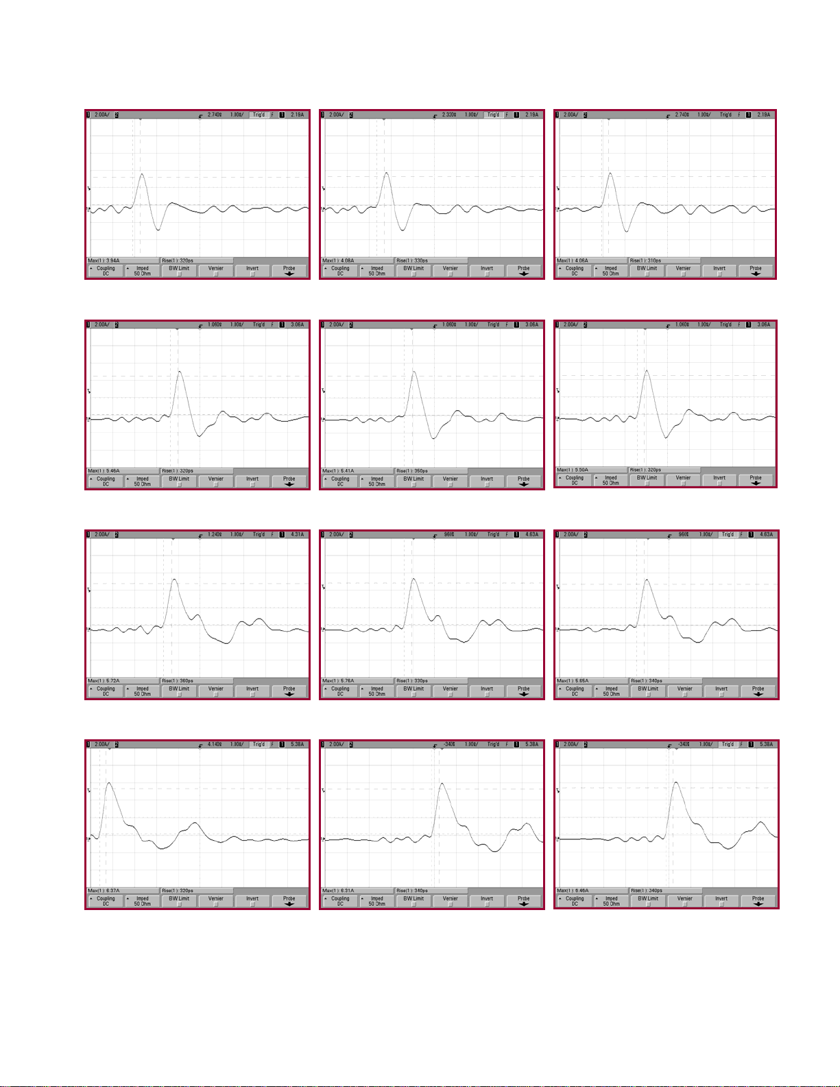
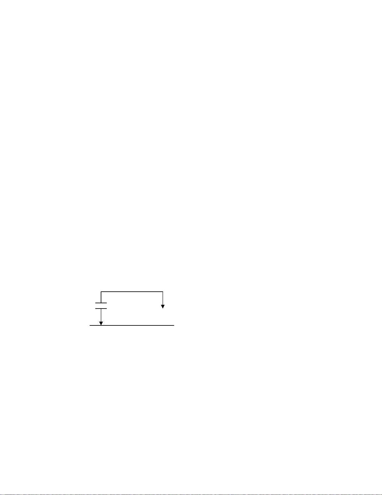
However, another type of discharge that is far more severe than the discharge from a
person touching a device is the Charge Device Model (CDM). This occurs when the device
itself becomes charged then touches ground a very fast rise time discharge can occur.
Charge
Touch to GND for discharge
GND
Figure 1.0-1: Basic Charge Device Model equivalent circuit
The CDM discharge is a function of the device capacitance that may be as low as a few
picofarads or can be as high as several hundred picofarads. This variation has a significant
affect on the severity of the discharge. Small component packages may not be able to hold
sufficient charge to meet specified discharge levels.
The Charged Device Model (CDM) test, as defined in standards JEDS22-C101C,
ANSI/ESD-STM 5.3 and AEC-Q101-005 describe a test procedure where a component is
slowly charged to a given voltage and then discharged to ground through one of the device
leads. The CDM test permits either field induced or direct charge/discharge.