Heathkit IO-4205 User manual

HEATHKIT
®
MANUAL
5 Megahertz
Dual Trace
Oscilloscope
Model 10-4205
595-2072
·.
'·
.
.·':::;_·.
7
...
~:···
...:::
.....
.
. ·
..
, ,,_
;~~:.
·.:
..
·
.:
..
·
::·.:.~--~
0
L~~-;·-~
HEATH
COMPANY
•
BENTON
HARBOR,
MICHIGAN

HEATH COMPANY PHONE DIRECTORY
The following telephone numbers are direct lines to the departments listed:
Kit orders and delivery information
...
.
....
.
......
..
. .
..
. (616) 982-3411
Credit
......
..
. .
......
.....
.......
..
.......
...
..
.
...
. (616) 982-3561
Replacement Parts .
....
.....
.....
. . .
...
..
.
..
..
.
..
..
...
(616) 982-3571
Technical Assistance Phone Numbers
8:
00A.M.
to
12
P.M.
and
1:00 P.
M.
to
4:30P
.M., EST, Weekdays Only
RtC, Audio, and Electronic Organs . .
..
. .
......
...
......
(616) 982-3310
Amateur Radio
.....
...
...
....
...
..
...
..
.....
...
......(616) 982-3296
Test Equipment, Weather Instruments and
Home Clocks . .
..
.
....
...
.......
. .
...
......
. .
..
. .
..
. (616) 982-3315
Television
..
.
....
.
....
..
. .
..
.
....
...
......
........
..
..
(616) 982-3307
Aircraft, Marine, Security, Scanners, Automotive,
Appliances and General Products
..........
......
•...
. (616) 982-3496
Computers
..
. .
..
.
....
...
. . .
..
.....
......
..
. .
..
.
...
..
. (616) 982-3309
YOUR HEATHKIT 90 DAY LIMITED WARRANTY
If
you are
not
satisfied
with
our
service- warrantyor
otherwise-
or
with
our
products, writedirectly to
our
DirectorofCustomer
Services, Heath Company, Benton Harbor,
Michigan
49022. He will make certain your problems receive
immediate,
personal
attention.
Our
attorney,
who
happens
to
be
quite
a kitbuilder himself, insists that
we
describe
our
warranty using all the necessary legal
phrases in order to
comply
with
the
new
warranty regulations. Fine. Here they
are
:
For a period ofninety (90) days after
purchase
, Heath
Company
will replace or repair free ofcharge any parts that are defective
either in materialsor workmanship. You
can
obtain parts directly from Heath
Company
by writing us at
the
address
below orby
telephoning
us at (616) 982-3571.
And
we'll
pay
shipping
charges to get those parts to
you-
anywhere
in
the world.
We
warrant
that
during
the first
ninety
(90) days after
purchase,
our
products,
when
correctly assembled, calibrated, adjusted
and
used in accordance with
our
printed
instructions, will meet published specifications.
If
a defective part or error in
design
has caused
your
Heathkit
product
to
malfunction
during
the
warranty period
through
no
fault of yours, we will service it free
upon
proof of
purchase
and
delivery at your expense to the Heath factory,
any
Heathkit
Electronic Center (units of Schlumberger
Products
Corporation). or
any
of
our
authorized
overseas distributors.
You will receive free
consultation
on
any
problem you
might
encounter
in
the
assembly or
use
of your Heathkit product. Just
drop us a
line
or give us a call. Sorry,
we
cannot
accept
collect calls.
Our
warranty does
not
cover
and
we
are
not
responsible for
damage
caused by
the
use of corrosive solder, defective tools,
incorrect assembly, misuse, fire, or by
unauthorized
modifications to or uses of
our
products for
purposes
other
than
as
advertised.
Our
warranty does
not
include
reimbursement
for
customer
assembly or set-up time.
~
This warrantycovers only Heathkit products
and
is not
extended
to allied
equipment
or
components
used in
conjunction
with
~
our
products. We
are
not
responsible
for
incidental
or
consequential
damages.
Some
states
do
not
allow
the
exclusion or
~
limitation of incidental or consequential damages, so
the
above limitation or exclusion may not
apply
to you. This warranty
gives you specific legal rights,
and
you may also have
other
rights
which
vary from state to state.
HEATH COMPANY ~
BENTON HARBOR, MI. 49022
~
oROOo&~uoOOOootooooomo~
Prices and specifications subject to change without notice.
Heathkit® Manual
HEATH
COMPANY
for
the
5 Megahertz
Dual Trace
Oscilloscope
Model 10-4205
595-2072
BENTON
HARBOR,
MICHIGAN
490
2 2
Copyright © 1978
Heath Company
All Rights Reserved
Printed in the United States of America

Page 2
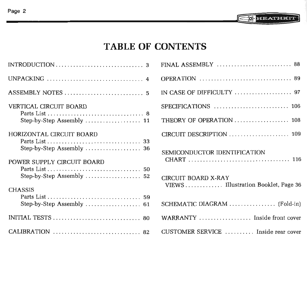
TABLE OF CONTENTS
INTRODUCTION o 0 0 0 0 0 0 0 0 0 0 0 0 0 o o o o 0 0 0 0 0 0 0 0 0 0 0 0 3
UNPACKING o o o o 0 0 0 0 0 0 0 0 0 0 0 0 0 o o 0 0 0 0 0 0 0 0 0 0 0 0 0 0 4
ASSEMBLY NOTES 0 o o o o o 0 0 0 0 0 0 0 0 o o o o 0 0 0 0 0 0 0 0 0 5
VERTICAL CIRCUIT BOARD
Parts List 0 0 0 0 0 0 0 0 0 0 0 0 0 0 0 0 0 0 0 0 0 0 0 0 0 0 0 0 0 0 0 0 0 8
Step-by-Step Assembly 0 0 0 0 0 0 0 0 0 0 0 0 0 0 0 0 0 0 0 11
HORIZONTAL CIRCUIT BOARD
Parts List 0 0 0 0 0 0 0 0 0 0 0 0 0 0 0 0 0 0 0 0 0 0 0 0 0 0 0 0 0 0 0 0 33
Step-by-Step Assembly 0 0 0 0 0 0 0 0 0 0 0 0 0 0 0 0 0 0 0 36
POWER SUPPLY CIRCUIT BOARD
Parts List 0 0 0 0 0 0 0 0 0 0 0 0 0 0 0 0 0 0 0 0 0 0 0 0 0 0 0 0 0 0 0 0 50
Step-by-
Step
Assembly 0 0 0 0 0 0 0 0 0 0 0 0 0 0 0 0 0 0 0 52
CHASSIS
Parts List 0 0 0 0 0 0 0 0 0 0 0 0 0 0 0 0 0 0 0 0 0 0 0 0 0 0 0 0 0 0 0 0 59
Step-by-Step Assembly 0 0 0 0 0 0 0 0 0 0 0 0 0 0 0 0 0 0 0 61
INITIAL TESTS 0 0 0 0 0 0 0 0 o 0 o o o 0 0 0 0 0 0 0 0 o o o o o o o 0 o 80
CALIBRATION 0 0 0 0 0 0 0 0 0 0 o o o 0 0 o 0 0 0 0 0 0 o o o o 0 0 0 0 82
FINAL ASSEMBLY o o 0 0 0 0 0 0 0 o o 0 0 o 0 0 0 0 0 o o o 0 0 0 0 88
OPERATION 0 0 0 0 0 0 0 0 0 o 0 0 0 0 0 0 0 0 o 0 0 o o o 0 0 0 0 0 0 o 0 89
IN
CASE OF DIFFICULTY 0 0 0 0 0 0 0 0 0 0 o o 0 0 0 0 0 0 0 o
97
SPECIFICATIONS 0 0 0 0 0 o o o 0 0 0 0 0 0 0 0 0 0 o o 0 0 0 0 0 0 106
THEORY OF OPERATION 0 o 0 o o o 0 o 0 o 0 0 0 0 0 o o 0 0 108
CIRCUIT DESCRIPTION o o o 0 0 0 0 0 0 0 0 0 0 o 0 0 0 0 0 0 0 109
SEMICONDUCTOR IDENTIFICATION
CHART 0 0 o o o o o o o 0 0 0 0 0 0 0 0 0 0 0 0 0 0 0 0 0 o 0 o 0 0 0 0 0 0 116
CIRCUIT BOARD X-RAY
VIEWS 0 0 0 0 0 0 0 0 0 0 0 0 0 Illustration Booklet, Page
36
SCHEMATIC DIAGRAM 0 0 0 0 0 0 0 0 0 0 0 o 0 0 0 0 (Fold-in)
WARRANTY 0 0 0 0 0 0 0 0 0 0 0 0 0 0 0 0 0 0
Inside
front cover
CUSTOMER SERVICE 0 0 0 0 0 0 0 0 0 0
Inside
rear cover

; ; :
INTRODUCTION
The
Heathkit
Model
10-4205, 5 MHz, Dual-Trace Os-
cilloscope is a compact, versatile, easy-to-build, elec-
tronic
instrument
that
you
can
use
to
study
the
waveforms
in
electronic circuits. You
can
also
use
it
to
measure
frequency,
and
AC or
DC
voltages.
The
DC
to 5 MHz
bandwidth
and
the
excellent
input
sensitiv-
ity of
the
vertical amplifiers
allow
you
to
use
this
Oscilloscopefor nearlyall
types
ofwaveform
applica-
tions
.
The
triggered
horizontal
sweep
circuit
and
the
many
other
outstanding
features
provide
accuracy
and
capabilities
that
are
usually
found
only
in
higher
priced
oscilloscopes.
Among
the
many
other
features
this
Oscilloscope of-
fers are:
• A
special
TV
position
on
the
triggerselector.
This
allows
low
frequencies
to
pass
while
rejecting
high
frequencies,
thus
making
it
Page 3
easier
to
trigger
on
the
vertical frequency of
a TV set.
• A
10
to
1
attenuation
circuit
that
can
be
used
for signals
applied
to
the
external, horizon-
tal
input
jack.
• Accurately calibrated vertical
attenuators
with
variable controls.
• A calibrated
time
base (seven
time
base
selections, variable
within
each selection).
These
features, along
with
the
attractive styling,
will
make
this
Oscilloscope a
welcome
asset to
the
laboratory, service shop, or
the
ham
shack
.

Page 4
UNPACKING
Inside
the
shipping
carton
was
the
box
stamped
PKl
which
contained
this
Assembly Manual.
With
this
box removed from
the
shipping
carton
,
you
will
find
bags
stamped
PACK 2
through
PACK 4.
The
Manual
will refer to these areas as
"packs."
You
will
be
di-
rected
to
open
each
of
these
"packs"
as
it
is needed.
All other parts
in
the
shipping
carton
will
be
consid-
ered
the
"final
pack."
Caution: Do
not
remove
any
partsfrom
their
bags or
the
"final
pack"
until
they
are
specifically called for
in
a Parts List
in
the
Manual.
Eachassembly section of
the
Manual
containsits
own
"Parts List"
and
"Step-by-Step Assembly" instruc-
tions.
At
the
beginning
of
each
"Parts
List," you
will
be
instructed
to
open
one
of
the
packs. You
will
also
be
directed,
in
some Parts Lists,
to
remove
certain
parts from
the
final pack.

Page 5
~~~~;allllll;ll:ll=u~
......................................................................
ASSEMBLY NOTES
TOOLS
You
will
need
these tools to assemble
your
kit
.
PLIER S
DIA
GON
AL
C
UTT
ERS
------------------------------------------------- H
EA
TH
KI T
SO
LD
ERING
I
RO
N
OTHER
HELPFU~
TOOLS
~
/
NUT S
TA
R
TER
1IMAY
BE
SUP
PLIED
I WITH" KI TI
I
I
DE
SO
LDE
RI
NG
BUL
B*
D
ESO
LDER
I
NG
BR
AID
*
OR
PE
NC
IL
SO
LD
ER
I
NG
I
RON
125
TO 40
WATT
S!
I * TO
REMOVE
S
OLDE
R
FROM
CIR C
UIT
C
ON
NEC
TI
ONS
.
·------------------------------------------------~
ASSEMBLY
1.
2.
Follow
the
instructions
carefully. Read
the
en-
tire
step before
you
perform
each
operation
.
The
illustrations
in
the
Manual
are called Picto-
rials
and
Details. Pictorials
show
the
overall op-
eration
for a
group
of
assembly
steps
; Details
generally
illustrate a
single
step.
When
you
are
directed
to refer to a
certain
Pictorial
"for
the
following
steps,"
continue
using
that
Pictorial
until
you
are referred
to
another
Pictorial for
another
group
of steps.
3.
4.
5.
Most kits
use
a separate
"Illustration
Booklet"
that
contains
illustrations (Pictorials, Details,
etc.)
that
aretoolargefor
the
AssemblyManual.
Keep
the
"Illustration Booklet"
with
the
As-
sembly
Manual.
The
illustrations
in
it are ar-
ranged
in
Pictorial
number
sequence.
Position
all
parts
as
shown
in
the
Pictorials.
Solder
a
part
or a
group
of
parts
only
when
you
are
instructed
to
do
so.

Page 6
6. Each circuit
part
in
an
electronickit
has
its
own
component
number
(R2, C4, etc.
).
Use
these
numbers
when
you
want
to
identify
the
same
part
in
the
various sections of
the
Manual.
These
numbers
,
which
are especially
useful
ifa
part
has
to
be
replaced
, appear:
In
the
Parts List,
At
the
beginning
of each step
where
a
component
is
installed,
In
some
illustrations,
In
the
Schematic,
In
the
section
at
the
rear of
the
Manual.
7.
When
you
are
instructed
to
cut
something
to
a
particular
length,
use
the
scales (rulers) pro-
vided
at
the
bottom
of
the
Manual
pages.
SAFETY WARNING:
Avoid
eye
injury
when
you
cut
offexcess
lead
lengths.
Hold
the
leads
so
they
cannot
fly
toward
your
eyes.
SOLDERING
Soldering
is one of
the
most
important
operations
you
will perform
while
assembling
your
kit. A good sol-
der
connection
will form
an
electrical
connection
be-
tween
two
parts
,
such
as a
component
lead
and
a
circuit
board
foil. A
bad
solder
connection
could
pre-
vent
an
otherwise
well-assembled kit from operating
properly.
It is easy to make a
good
solder
connection
if you
follow a few
simple
rules:
1.
2.
Use
the
right
type
of
soldering
iron. A
25
to
40-watt
pencil
soldering
iron
with
a
1/8"
or
3/16"
chisel or
pyramid
tip
works best.
Keep
the
soldering
iron
tip
clean.
Wipe
it often
on
a
wet
sponge
or
cloth
;
then
apply
solder
to
the
tip
to give
the
entire
tip
a
wet
look.
This
process is called
tinning
,
and
it
will protect
the
tip
and
enable
you
to
make
good
connections
.
When
solder
tends
to
"ball"
or does
not
stickto
the
tip,
the
tip
needs
to
be
cleaned
and
retin-
ned.

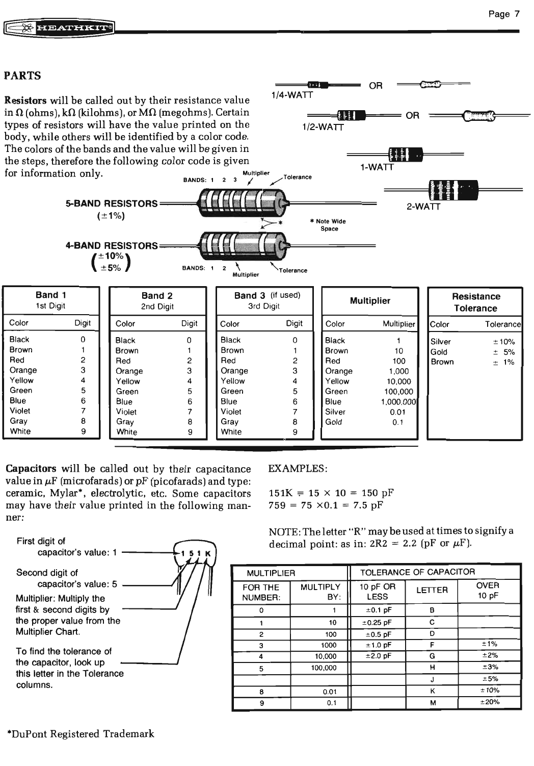
PARTS
Resistors
will
be
called
out
by
their
resistance
value
in
0 (ohms),
kO
(kilohms), or
MO
(megohms). Certain
types of resistors
will
have
the
value
printed
on
the
body,
while
others
will
be
identified
by
a color
code
.
The colors of
the
bands
and
the
value
will
be
given
in
the
steps, therefore
the
following color
code
is given
Page 7
==
OR
1/4-WATT
==fllm-===OR~
1/2-WATT
for
information
only.
Multiplier
BANDS
: 1 2 3 / /Tolerance 1-WATT
*Note
Wide
Space
=======~--~=
2-WATT
Band 1 Band 2 Band 3 (if used)
Multiplier
Resistance
1st Digit 2nd Digit 3rd Digit
Color Digit Color Digit Color
Black 0 Black 0 Black
Brown 1 Brown 1 Brown
Red 2 Red 2 Red
Orange 3 Orange 3 Orange
Yellow 4 Yellow 4 Yellow
Green 5 Green 5 Green
Blue 6 Blue 6 Blue
Violet 7 Violet 7 Violet
Gray 8 Gray 8 Gray
White 9 White 9 White
Capacitors
will
be
called
out
by
their
capacitance
value
in
JLF
(microfarads) or
pF
(picofarads)
and
type:
ceramic, Mylar*, electrolytic, etc.
Some
capacitors
may
have
their
value
printed
in
the
following
man-
ner
:
Digit Color Multiplier
0 Black 1
1 Brown 10
2 Red 100
3 Orange 1,000
4 Yellow 10,000
5 Green 100,000
6 Blue 1,000,000
7 Silver 0.
01
8 Gold 0.1
9
EXAMPLES:
151K
=:=
15
X
10
=
150
pF
759
=
75
X0.1
= 7.5
pF
Tolerance
Color Tolerance
Silver
:!:
10%
Gold
:!:
5%
Brown
:!:
1%
First digit of
capacitor's value: 1
NOTE:
The
letter"R"
may
be
used
at
times
to
signifya
decimal
point: as in: 2R2 = 2.2 (pF or
JLF).
Second digit of
capacitor's value: 5
____
_,
Multiplier: Multiply the
first & second digits by
the proper value from the
Multiplier Chart.
To find the tolerance of
the capacitor, look up
this letter
in
the Tolerance
columns.
*
DuPont
Registered
Trademark
MULTIPLIER
FOR THE
NUMBER:
0
1
2
3
4
5
8
9
MULTIPLY
BY:
1
10
100
1000
10,000
100,000
O.D1
0.1
TOLERANCE OF CAPACITOR
10 pF OR LETTER OVER
LESS 10 pF
±0.1
pF
B
±0.
25
pF
c
±0.5
pF
D
±1.0
pF
F
:±
1o/o
±2.0
pF
G ± 2°/o
H ±3
o/o
J ±5°/o
K ±
10%
M ±
20%

Page
8
VERTICAL
CIRCUIT
BOARD
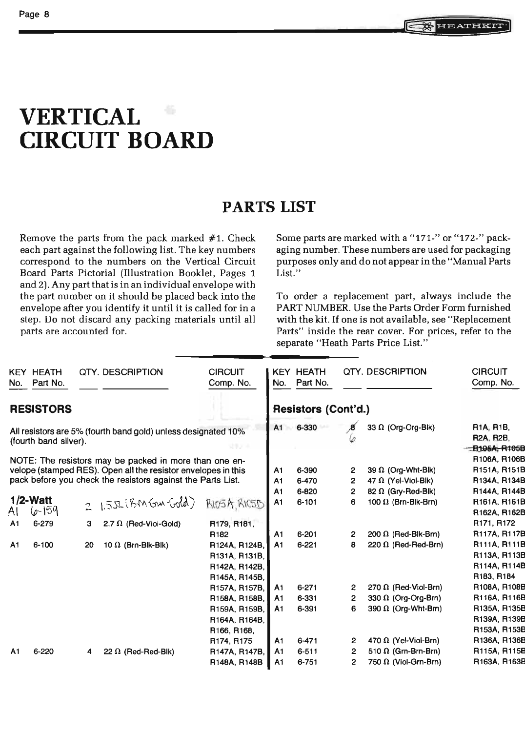
PARTS LIST
Remove
the
parts from
the
pack
marked
#1.
Check
each
part
against
the
following list.
The
key
numbers
correspond
to
the
numbers
on
the
Vertical Circuit
Board Parts Pictorial (Illustration Booklet, Pages 1
and
2).
Any
part
that
is
in
an
individual
envelope
with
the
part
number
on
it
should
be
placed
back
into
the
envelope
after
you
identify
it
until
it
is called for
in
a
step. Do
not
discard
an
y
packing
materials
until
all
parts are
accounted
for.
KEY
HEATH
QTY.
DESCRIPTION
CIRCUIT
No. Part
No
. Comp. No.
RESISTORS
All resistors
are
5%
(fourth
band
gold)
unless
designated
1
0%
(fourth
band
silver).
NOTE
:
The
resistors
may
be
packed
in
more
than
one
en-
velope
(stamped
RES).
Open
all
the
resistor
envelopes
in
this
pack
before
you
check
the
resistors
against
the
Parts List.
1/2-Watt 2 \.S
3L
\
Y
;
·
tV\-G
M
~
)
~
tcf-i
~
I
R
\05~
AI
(p-
15q
A1
6-279 3 2.7 n (Red-Viol-Gold) R179,
R181,
R182
A1
6-100 20
10
n (Brn-Bik-Bik) R124A, R124B,
R131A, R131B,
R142A, R142B,
R145A, R145B,
R157A, R157B,
R158A, R158B,
R159A, R159B,
R164A, R164B,
R166, R168,
R174
, R175
A1
6-220 4
22
n (Red-Red-Bik) R147A, R147B,
R148A, R148B
Some
parts
are
marked
with
a "
171-
" or
"172-
" pack-
aging number.
These
numbers
are
used
for packaging
purposes
only
and
do
not
appear
in
the
"
Manual
Parts
List."
To order a
replacement
part, always
include
the
PART NUMBER. Use
the
Parts
Order
Form
furnished
with
the
kit
.
If
one
is
not
available, see "Replacement
Parts"
inside
the
rear cover.
For
prices, refer to
the
separate "
Heath
Parts Price List."
KEY
HEATH
QTY.
DESCRIPTION
CIRCUIT
No.
Part
No
. Comp.
No
.
Resistors (Cont'd.)
A1
6-330 {
33
n (Org-Org-Bik)
R1A
,
R1B
,
R2A
,
R2B
,
::::ftj:()
SA
, R4059;
R106A, R106B
A1
6-390 2 39 n (Org-Wht-Bik) R151A, R151B
A1
6-470 2 47 n (Yei-Vioi-Bik) R134A, R134B
A1
6-820 2
82
n (Gry-Red-Bik) R144A, R144B
A1
6-101
6 100 n (Brn-Bik-Brn) R161A,
R16
·
1B,
R162A, R162B,
R171,
R172
A1
6-201
2 200 n (Red-Bik-Brn) R117A, R117B
A1
6-221
8 220 n (Red-Red-Brn) R111A, R111B,
R113A, R113B,
R114A, R114B,
R183,
R184
A1
6-271
2
270
n (Red-Vioi-Brn) R108A, R108B
A1
6-331
2 330 n (Org-Org-Brn) R116A, R116B
A1
6-391
6 390 n (Org-Wht-Brn) R135A, R135B,
R139A, R139B,
R153A, R153B
A1
6-471
2 470 n (Yei-Vioi-Brn) R136A, R136B
A1
6-511
2
510
n (Grn-Brn-Brn) R115A, R115B
A1
6-751
2 750 n (Vioi-Grn-Brn) R163A, R163B

Page 9
®
~
f§
1
%f#fB+@
KEY
HEATH QTY. DESCRIPTION CIRCUIT KEY HEATH QTY. DESCRIPTION CIRCUIT
No
. Part No. Comp. No. No. Part No. Comp.
No.
Resistors (Contd.) Capacitors, Ceramic (Cont'd.)
A1
6-102 20 1000 n (8rn-81k-Red) R104A, R1048;
81
21-141 1 .0033
JLF
C131
R133A, R1338,
81
21
-27 4 .005
JLF
C107A, C1078,
R141A, R1418, C135, C136
R146A, R1468,
81
21-47 3 .
01
JLF
C109A, C1098,
R149A, R1498, C122
R156A, R1568,
81
21
-
31
.02
JLF
C124
R165, R167,
81
21-199 2 .1
JLF
C114A, C1148
R185, R186,
R187, R188, Electrolytic
R191
, R192
A1
6-122 2 1200 n (8rn-Red-Red) R155A, R1558 82 25-115 8
10
JLF
C111A, C1118,
A1
6-182 2 1800 n (8rn-Gry-Red) R137A, R1378 C113A, C1138,
A1
6-272 4 2700 n {Red-Viol-Red) R118A, R1188, C123, C132,
R122A, R1228 C133, C134
A1
6-332 4 3300 n (Org-Org-Red) R119A, R1198,
83
25-117 4 100
JLF
C118A, C1188,
R121A, R1218 C119A, C1198
A1
6-912 2 9100 n (Wht-8rn-Red) R103A, R1038
B3
25-160 3 250
JLF
C125, C126,
A1
6-103 4
10
kfi
(8rn-81k-Org) R109A, R1098, C127
R154A, R1548
A1
6-153 2 15
kfi
(8rn-Grn-Org) R132A, R1328 Trimmer
A1
6-223 22
kfi
(Red-Red-Org) R169
A1
6-913 2
91
kfi
(Wht-8rn-Org) R102A, R1028
84
31-56 4 1.
5-
20 pF C101A, C1018,
A1
6-104 2 100
kfi
(8rn-81k-Yel) R107A, R0178 C103A, C1038
A1
6-914 2 910
kfi
(Wht-8rn-Yel) R101A, R1018
84
31
-
54
2 4-40
pF
C102A, C1028
84
31-52 4 8-60
pF
C104A, C1048,
C115A, C1158
Other Resistors
85
31-77 2 80-400
pF
C106A, C1068
6-1801-
~
'/t..j
A2
4 1800 n (1.8
k)
~
watt
,
R123A, R1238,
IZ.
1%
(8rn-Gry-81k-8rn) R127A, R1278 Other Capacitors
A2
6-4320-11 4 432 n' 1/8-watt, 1% R125A, R1258,
(Yei-Org-Red-81k) R126A, R1268 86 27-28 2 .1
JLF
Mylar
C1
,
C2
A3
1-19-1 220 n,1-watt, 10% R173
{Red-Red-8rn)
A4
5-11-2 15
kfi
, 2-watt, 10% R176
(8rn-Grn-Org) DIODES
AS
3-55-5 2 2000 n
(2
k), 5-watt R177, R178
C1
56-56
~
1N4149
g~e~A
.
o~e+So
CAPACITORS \(o 9Hl2A., 0192&,-
0103A, 01038,
Ceramic 0104A,
01048
,
0105A,
01058
,
81
21-7 2 33 pF C117A, C1178 0106A,
01068
,
81
21-121 4
56
pF C112A, C1128, 0108A,
01088
,
C116A, C1168 0109A,
01098
,
81
21-75 1 100 pF
C121
0111A,
01118
,
81
21-722 2 330 pF C105A, C1058 0112A,
01128
81
21-140 2 .
001
JLF
C128, C129
C1
56-67 VR10A 0107
81
21-36 2 .002
JLF
C108A, C1088
C1
56-89 4 G0510 0113, 0114,
0115,0116

Page
10
KEY HEATH
QTY.
DESCRIPTION
No. Part
No.
CIRCUIT
Comp.
No.
TRANSISTORS-INTEGRATED CIRCUITS (IC's)
NOTE:Transistors and integrated circuits are marked for iden-
tification
in
one
of
the following four ways:
1.
Part Number.
2.
Type number.
(On
integrated circuits, this refers
only to the numbers and letters listed. Any addi-
tional letters or numbers
on
an
IC
are not signifi-
cant.)
3. Part number
and
type number.
4.
Part number with atype number other than the one
listed.
01 417-235 8 2N4121 transistor
01 417-237 2 SE6020 transistor
01 417-260 4 2N4258A transistor
01 417-293 4 2N5770 transistor
01 417-801 4 MPSA20 transistor
02
417-834 2 MPSU10 transistor
03
417-902 4 5566 transistor
04
443-1 7400 IC
04
443-4 1 7472 IC
pi
LJll-
~Lf
1../
"=>e1
eo
tfl.!M!?
Is
'\tJ
f
OTHER CIRCUIT COMPONENTS
E1
10-357
E2 10-917
E2
E2
E3
E4
E5
E6
E7
10-918
10-936
10-1118
60-73
60-624
63-1316
475-16
HARDWARE
#4
Hardware
F1
250-428
F2 250-52
F3 250-186
F4 252-15
F5 254-9
2 100 n control
3 200 n control
2
2
2
2
1
2
2
500 n control
1000
ll
(1K) control
1000
ll
(1K) control
DP3T 3-position slide switch
DP4T 4-position slide switch
Rotary switch with 5000 n
(5K) control
Ferrite bead
1 4-40 x 1/4" flat head screw
2 4-40 x 1/4" screw
4
#4
x 3/8" screw
3 4-40 nut
3
#4
lockwasher
0
Y.
}'2
"/.
(I
N C
HES
) 2
0106A
,
01068
1
0107A
I
01078
1
01
08A,
01088
1
0109A
I
01098
0113
1
0114
0104A
,
01048
,
01
05A,
01
05B
0111A
,
01118
,
0112A
, 0 1
128
0103A
, 0 1
038
,
0117
,
0118
0115
,
0116
0101A
,
01018
,
0102A
,
01028
U101
U102
DID\
1::>10\5
)
DIDZ.AJ
"))l
Z!S
R112A, R112B
R152A, R152B,
R189
R143A, R143B
R138A, R138B
R4A, R4B
SW1A, SW1B
SW3
SW2A-R3A,
SW2B-R3B
3
KEY HEATH QTY. DESCRIPTION
No. Part
No.
#6
Hardware
G1
250-1282 3 6-32 x 1/8" black setscrew
G2 250-33 4 6-32 x 1/8" setscrew
G3 250-416 4 6-32 x 1/4" flat head screw
G4 250-56 4 6-32 x 1/4" screw
G5
252-3 4 6-
32
nut
G6 254-1 4
#6
lockwasher
Other Hardware
H1
253-50 2 1/4" plastic spacer
H2 252-7 4 3/8-32 nut
H3 255-145 2 3/8" spacer
MISCELLANEOUS
J1
75-769
J2 75-770
J3 266-1008
J4
J5
J6
J7
85-2043-1
204-2315
204-2333
206-1273
215-95
343-15
344-
51
346-1
347-55
390-1436
J8 432-892
J9 434-230
J10 434-298
J11
453-66
J12 455-44
J13 456-7
J14 462-1049
J15 462-1050
J16 462-1055
L1 490-5
134-237
L2
260-16
L3 73-34
390-147
390-1255
390-1483
391-34
597-260
4
Slide switch cover
(1
-7
/1
6")
Sl
i
de
switch cover (29/32")
Slide switch cover
(1
-3/16")
Vertical circuit board
Sw
itch bracket
2 Control bracket
1 Circuit board shield
2 Heat sink
4' Shielded cable
3' Brn wire
8-1
/2" Sleeving
1-1
/2' a-conductor flat cable
1 Metal front panel
2 BNC connector
4 8-pin IC socket
2 14-pin IC socket
2 5" extension shaft
2 Split plastic bushing
2 Shaft coupling
Red knob
2 Small black knob
Large black knob
Plastic nut starter
1 Cable with connector
2 Alligator clip
2 Red alligator clip insulator
Danger label
Fuse label
Power consumption label
Blue and white label
Parts Order Form
Solder
Assembly Manual (See Page 1
for Part Number)
5 6
I1
(8
I
3~ 8
I " (8 I 7
~
8
I .I I I I I I
I"'
I
IIII
1 I I I ' I I
,.
1, I I I I I I I I I I I I ' I
·,I
I
I'
I l ' I I I
I ' I I ' I I I
I
Q .
!5
1
(C
M )
'2
3
I'
"
'I
e 7 · e ' I
9 I
10 11
12
13
1 4
15
,.,
CIRCUIT
Comp.
No.
J1
, J2
7
'II
I
17

In
the
following steps, you will be
given detailed
instructions
on
how
to
install
and
solder
the
first
part
on
the
circuit
board. Read
and
perform each
step carefully.
Then
use
the
same
pro-
cedure
whenever
you install parts
on
a
circuit
board.
NOTE: Only a
portion
of
the
circuit
board is
shown
in
some of
the
follow-
ing Pictorials.
The
small
"Identifica-
tion
Drawing" at
the
top of
the
page
shows
the
area
ofthe
circuit
boardtobe
assembled.
( ) Position
the
circuit board as
shown
with
the
printed
side
(not
the
foil side) up.
NOTE:
When
you
install a
component
that
has its
value
printed
on
it,
position
the
value
marking
up,
so it
can
be eas-
ily
read
. Diodes
should
be
mounted
with
their
type
or
part
number
up,
if
possible.
Hold
a 910
k.O
(Wht-Brn-Yel) re-
sistor
with
long-nose pliers
and
bend
the
leads
straight
down
to fit
the
hole
spacing
on
the
circuit
board
.
( ) R101B:
Push
the
leads
through
the
holes at
the
indicated
location
on
the
circuitboard.
The
end
with
color
bands
may
be
positioned
either
way
.
Press
the
resistor
against
the
cir-
cuit
board.
Then
bend
the
leads
outward
slightly to
hold
the
resis-
tor
in
place
.
STEP-BY-STEP ASSEMBLY
Page
11
IDENTIFICATION
DRAWING
CONTINUE<:/
The
steps performed
in
this Pictorial are
in this area of
the
circuit
board.
PICTORIAL 1-1
( )
Turn
the
circuit
board over
and
solder
the
resistor leads to
the
foil
as follows:
1.
Push
the
soldering
iron
tip
against
both
the
lead
and
the
circuit board foil. Heat both
for
two
or
three
seconds.
SOLDERING
iRON
COMPONENT
/)
LEAD
w
~~~
BOARD
2.
Then
apply
solder to
the
other
side
of
the
connection
.
IMPORTANT: Let
the
heated
lead
and
the
circuitboard foil
melt
the
solder.
SOLDERING
IRON
SOLDER
FOIL'\_
3. As
the
solder begins to melt,
allow it
to
flow
around
the
connection
.
Then
remove the
solder
and
the
iron
and
let
the
connection
cool.
FOIL
SOLDERING
IRON
( ) Cut off
the
excess lead lengths
close to
the
connection
. WARN-
ING: Clip
the
leads so
the
ends
will
not
fly toward
your
eyes.
( ) Check each connection. Compare
it to
the
illustrations
on
Page
12
.
After you have checked
the
solder
connections, proceed
with
the
as-
sembly
on
Page 13. Use
the
same
soldering
procedure
for each
connection
.

Page 12
A GOOD SOLDER CONNECTION
~-------------------,
S
OLDER
FLOWS
OUTWARD
AND
GRADUALLY
BLEND
S
WITH
THE
FOIL
AND
THE
LE
AD
.
,')
/
,'
/
//
,(_;;
OLDER
IN G
',,
IRON
,~;~
P
OS
ITIO
N
ED
CO
RR
EC
TL
Y
I
I
I
I
I
When
you
heat
the
lead
and
the
circuit
board
foil at
the
same
I
time
,
the
solder will flow
evenly
onto
the
lead
and
the
foil. I
1
The
solder
will make a
good
electrical
connection
between
I
Lt~
~~~
~
!!!i~
___________
-~
POOR
SOLDER CONNECTIONS
~----------------------------~-----,
I
SOL
DE
R DOES
NO
T
FL
OW / / I
ONT
O
LEA
D. A
DAR
K
RO
S
IN
,
,')
,'
SOLDERING
I BEAD SURROUN DS
AND
IN-
//
,'
SO
LD
ER
APPEARS
TO
FLOW
//,.
-
........_
IRON
I SUL
ATE
S THE L
EA
D
FRO
M
ROS
IN
,<;
, IN
WA
RD
AND S
ET
ON
TOP
/ ,
',
PO
SIT IONED
T
HE
CONNECT I
ON
.
//,'S
OLDERING OF
TH
E
FO
IL
.
//,'
IN
CO
RRE
C
TL
Y
'
''
""
IRON '
I
FO
IL
//•
PO
S
ITIO
N
ED
I
,,,
, I NC
ORRE
C
TL
Y
I
When
the
lead
is
not
heated
sufficiently,
the
solder
I
will
not
flow
onto
the
lead as
shown
above. To cor-
When
the
foil is
not
heated
sufficiently
the
solder
will
blob
on
the
circuit
board
as
shown
above. To correct,
1 rect,
reheat
the
c
onnection
and
,
if
necessary,
apply
a reheat
the
connection
and
, ifnecessary,
apply
a small 1
1
small
amount
of
additional
solder
to obtain a good
amount
of
additional
solder
to obtain a good connec- I
Lc~~c~r:_
_____________
_!~;....
______________
.J
.~
SOLDER BRIDGES
A
solder
bridge
between
two
adjacent
foils is
shown
in
photograph
A.
Photograph
B
shows
how
the
con-
nection
should
appear. A
solder
bridge
may
occur
if
you
accidentally
touch
an
adjacent
previously
sol-
dered
connection,
if
you
use
too
much
solder, or if
you "drag"
the
soldering
iron
across
other
foils as you
remove
it
from
the
connection
. A good
rule
to follow
is:
alwa
ys take a good look
at
the
foil area
around
each
lead before
you
solder
it.
Then
,
when
you
solder
the
connection
, make
sure
the
sold
er
remains
in
this
area
and
does
not
bridge
to
another
foil.
This
is especially
important
when
the
foils are small
and
close together.
NOTE:
It
is alright for
solder
to
bridge
two connec-
tions
on
the
same foil.
Use
only
enough
solder to
make
a good
connection
,
and
lift
the
soldering
iron
straight
up
from
the
circuit
board
.
If
a
solder
bridge
should
develop,
turn
the
circuit
board
foil-
side-down
and
heat
the
solder
be-
tween
connections.
The
excess
solder
will
run
onto
the
tip
of
the
soldering
iron
,
and
this
will
remove
the
solder
bridge
. NOTE:
The
foil
side
of
most
circuit
boards
has a coating
on
it
called
"
solder
resist."
Th
is
is a protective
insulation
to
help
prevent
solder
bridges.
B
A
SOLDER
BRIDGE

::
::
::
The
steps performed in this Pictorial a
re
in this area of
the
circuit board.
--~,.-fi
Be sure you
installed
resistor
in
Pictorial 1-1 (Page 11).
R102B:
91
kfl (Wht-Brn-Org).
R105B: 1.5 0 (Brn-Grn-Gold).
NOTE: Your circuit board
may
be
marked 33 at
this
location.
R104A: 1000 0 (Brn-Blk-Red).
R105A: 1.5
tf
(Brn-Crn-Go1d).
NOTE: Your circuit board
may
be
33
at
this
location.
Solderthe leads to
the
foil
and
cut
off the excess
lead
lengths
.
NOTE: When you install a diode, al-
ways
match
the
band
onthe
diode
with
the
band
mark on
the
circuit board. A
DIODE
WILL
NOT WORK PROPERLY
IF
IT
IS
INSTALLED BACKWARDS.
See Detail 1-2A.
BAN:~
}/
'¥-
NO
·
··
:·::
:-:.:·
:·:·:"
··BAND
GLASS'--..
BODY
COLORED
END
If
your
diode
hasa solid
body
,
the
band
is clearly defined.
If
your
diode
has a
glass
body
,
do
not mistake the colored
end
inside
the diode for the
banded
end
. Look for a
band
painted
on
the
outside
of the glass.
)
PART
NUMRER
PICTORIAL 1-2
Page 4 of 5
10-4205/595-2072
591-3025
IDENTIFICATION
DRAWING
Page
13
07B: 100 kfl (Brn-Blk-
Yel)
.
01B:
Selected
transistor
(#417-854). See Detai11-2B.
""""
'""',"~the
leads to
the
foil
and
cut
excess lead
lengths
~
: 100 kfl (Brn-Blk-
Yel)
.
U
··
1
ho1A:
Selected
transistor
(#417-854). See Detail1-2B.
Soldertheleads to thefoil and cut
off the excess lead lengths.
IMPORUNT:
THE
BANDED
END
OF
DIODES
CAN
BE
MARKED
IN
A
NUMBER
OF
WAYS.
~
BANDED
END
.._
___
Detail1-2A
__
_

Page 14
The
steps performed in
this
Pictorial are
in
this area of the
circuit
board.
--~---~.....:;
178: 200
.n
(Red-Blk-Brn).
168: 330
.n
(Org-Org-Brn).
1278: 1800
.n
(1.8 k). 1% (Brn-
Gry-Blk-Brn). '
/4
~
1158: 510
.n
(Grn-Brn-Brn).
1148: 220
.n
(Red-Red-Brn).
Solder the
leads
to
the
foil
and
cut
off the excess
lead
lengths
.
17
A:
200
.n
(Red-Blk-Brn).
R116A: 330
!l
(Org-Org-Brn).
NOTE:
When
a
bar
e wire is
called
for
in
a step,
remove
all
the
insu
l
ation
from
the
specified l
ength
of
brown
wire.
0
1"
bare wire.
R125A: 432 .0 , 1% (Yel-Org-Red-
Blk).
R126A: 432 .0, 1% (Yel-Org-Red-
Blk).
R115A: 510
.n
(Grn-Brn-Brn).
R114A: 220
.n
(Red-Red
-B
rn).
R113A: 220
!l
(Red-Red-Brn).
Sol
der
the
leads to
the
foil
and
cut
off the excess lead lengths.
y.
Yo
:y.
1
(I
N C H
IE
S)
2
I1( 8 I
3~ 8
I
~
(
8
I
1;
8 1 I I
I I I
I I I I I I
iif
l
jiill)
0 .e 1 (
CM
) 2 3 4 e I
I I I I I
I I I
8 7 I
IDENTIFICATION
DRAWING
PART
NUMBER
c=:>
r-----l
I I
: I
I I
I I
I I
I
I
I
I
I
PICTORIAL 1-3
3 4
I I
II I I I I I I I I II I
I I I
I
8 " 10 ,
12
CONTINUEO
IDENTIFIC
DRAWl
I I
NOTE:
When
a
wire
is called for
in
a
step,
cut
the
brown
wire
to
the
specified length.
Then
remove
1/4" of
insulation
from
each
end.
5
I
2-1/4" Brn
wire
.
D104B: 1N4149
diode
(#56-56).
D103B: 1N4149
diode
(#56-56).
R118B: 2700
!l
(Red-Viol-Red).
R126B: 432 .0, 1% (Yel-Org-Red-
Blk).
R125B: 432 .0 , 1% (Yel-Org
-R
ed-
Blk).
R124B: 10
!l
(Brn-Blk-Blk).
R127A: 1800
.n
(1.8 k). 1% (B
rn
-
Gry-Blk-Brn). '
/'1
~
R123A: 1800
!l
(1
.8 k), 1% (Brn-
Gry-Blk-Brn).
'/~
~
Sol
der
the
leads
to the foil
and
cut
the
excess
lead
lengths.
R122A: 2700
!l
(Red-Viol-Red).
R136A: 470
.n
(Yel-Viol-Brn).
nP
, n r
n<>
r
the
l
eads
to
the
foil
and
cut
off
the
excess
lead
lengths.
6
I
I I I I I I I I II I I I I
I I I
13 14 18
18 17
7
I

The
ste
ps
performed
in
this Pictorial are
in
this area of
the
circuit
board.
R136B: 470 0 (Yel-Viol-Brn).
R137B: 1800 0 (Brn-Gry-Red).
1000 0 (Brn-Blk-Red).
1800 0 (Brn-Gry-Red).
Solder
the
leads
to
the
foil
and
cut
off
the
excess lead
lengths
.
PICTORIAL 1-4
IDENTIFICATION
DRAWING
Page
15
: 82 0 (Gry-Red-Blk).
1000 0 (Brn-Blk-Red).
82
0 (Gry-Red-Blk).
R154A: 10 0 (Brn-Blk-Blk).
R147A:
22
0 (Red-Red-Blk).
Solder
th
e leads to
the
foil
and
cut
off
the
excess lead l
engt
hs
.

1
Page
16
The
steps
performed
in
this Pictorial are
in
this
area of
the
circuit board.
100
fi
(Brn-Blk-Brn).
: 100 n (Brn-Blk-Brn).
Solder the leads to
the
foil
and
cut
off the excess lead lengths.
R146A: 1000
fi
(Brn-Blk-Red).
149A: 1000 n (Brn-Blk-Red).
R155A: 1200
fi
[Brn-Red-Red).
R151A: 39
fi
(Org-Wht-Blk).
R154A: 10
k!l
(Brn-Blk-Org).
Solder
the
leads
to
the
foil
and
cut
off
the
excess
lead
lengths
.
PICTORIAL 1-5
PART
NUMBER
R154B: 10
k!l
(Brn-Blk-Org).
R187: 1000
fi
(Brn-Blk-Red).
D111B: 1N4149
diode
(#56-56).
R159B: 10 n (Brn-Blk-Blk).
;Y
Solder
the
leads
to
the
foil
and
cut
off
the
excess lead lengths.
./
J
Solder
the
leads to
the
foil
and
cut
off
the
excess lead
lengths
.
(Wt"S}

IDENTIFICATION
DRAWING
Page 17
PART
--------~----~-
NUMBER
~-;-~---
The
steps performed
in
this Pictorial are
D113: GD510
diode
(#56-89).
( ,..YR192: 1000 n (Brn-Blk-Red).
(
,)--
R186: 1000 n (Brn-Blk-Red).
(
vJ'
R188: 1000 n (Brn-Blk-Red).
R185: 1000 n (Brn-Blk-Red).
Solder
the
leads
to
the
foil
and
cut
off
the
excess
lead
lengths
.
166: 10 n (Brn-Blk-Blk).
10 n (Brn-Blk-Blk
).
Solder
the
leads
to
the
foil
and
cut
off
the
excess
lead
lengths
.
O
y.y,•;.
1
I
1[8
I
•;
aI
5[B
I
7ta
I
l i
flj
lll
ij
I I I '
Q ·5 1
(CM)
2
( I
NCHES)
I I I I I I
I
3
2
I
I II I I
"
l
L.__
__
~
PICTORIAL
1-6
3 4
I I I I
I I I I I I I I
I I
8 9
10
,
in
this area of
the
circuit
board.
II I I
I I I I
12
: 2.7 n (Red-Viol-Gold).
79
: 2.7 n (Red-Viol-Gold).
: VR10A
diode
(#56-67).
9:
22
kn
(Red-Red-Org).
(
~
Solder
the
leads to
the
foil
and
cut
off
the
excess
lead
lengths
.
5 6
I I I
I I I I I I I
I I I
I I I
13 14 15
1<0
17
7
I

Page
18
The
steps performed in this Pictorial are
in this area of the circuit board.
......--~
START•
) Reposition the circuit board as
shown. Solder
the
pins
to
the
foil !DENT!FICATION
as you install each part.
ORA
WING
NOTE: When you install
an
IC
socket,
insert the pins
into
the circuit b.oard
holes.
The
index mark on
the
circuit
board
must
still be visible after
the
socket is installed.
IC
socket at
QlOlA.
in
IC
socket at Q102A.
in
IC
socket at U102.
14-pin
IC
socket at U101.
Q
~
nc=:>
~I
PART
NUMBER
PICTORIAL
1-7
CONTI
NU
Ev
NOTE: When you install a control, in-
sert
the
pins
into
the
circuit
board
holes
and
solder them to
the
foil.
~
1
..
..
~
...
....
.•
,.;ip'i''>
100 n control (#10-357).
Table of contents
Other Heathkit Test Equipment manuals