Heathkit OM-3 Guide

Assembling
qnd Using YourGGG
oscrLLoScoPE
MODET OM.3
-

J
i
;I
a
MODEL OM-3
ASSEMBLY AND OPERATION OF THE
HEATHKIT OSCILLOSCOPE
SPECIFICATIONS
Vertical:
Rise Time
Frequency Response
Sensitivity
Input Impedance at 1 kc.
Horizontal:
Frequency Response
Sensitivity
Input Impedance
Sweep Generator: ....
Astigmatism (Spot Shape):
Tube Complement:
0.25 microseconds
13 DB 4 cps 1.2 megacycles
tG DB 3 cps to 2 megacycles
0.09 nMS volts per inch at 1 kc
2.6 megohms at Xl
3.3 megohms at X10 and X100
These impedances are the result of-22 1,t1tf- shunt-
ing 3. 6 megohtns at X1, and 11 pipf shunting 3. 9
megohms at X10 and X100.
t3 DB'2 cps to 425 kc
+6 DB I cps to 650 kc
0.275 RMS volts per inch at 1 kc
25 ttttf.d shunting 10 megoh-ms
Multivibrator 20 cPs to over 150 kc
Control on chassis
One 5BP1 cathode ray tube
Two 12AU? horizontalcathode follower and am-
plifier. Horizontal deflection amplifier
One 128H7 vertical deflection amplifier
One 68A8 vertical cathode follower and amplifier
One 12AX7 sweep multivibrator
One 6X4 low voltage rectifier
One 1V2 high voltage rectifier
i
I
r
I
I
{

E
-
i' ,l
s
(0x
>@
@o
>o
nso
551'
JHI''
eqo
T--l(--ll',
I ido
JF-ll,'
FN
ir
F] ga?
R=
:o
?-i J
X.'
\., o
g=
Er
s
I
Hl"
z
:U
I
I
/t
ts'
l
N
ts
x
O<
o
a
t
3
:=
?Br.
HVvlArlll'
I'
6
:i L-
t
o
t---l | | r
\t,
I il,,
relll
\a8''
r!
o-l
;" 3l
/r lt,,t9\l i
'! ,
-:s.YE
-i9 _
t fd"-:
q 6- -
az24
! frs:
'F!- 6
filt
;E
!
*-ltr
Page 2

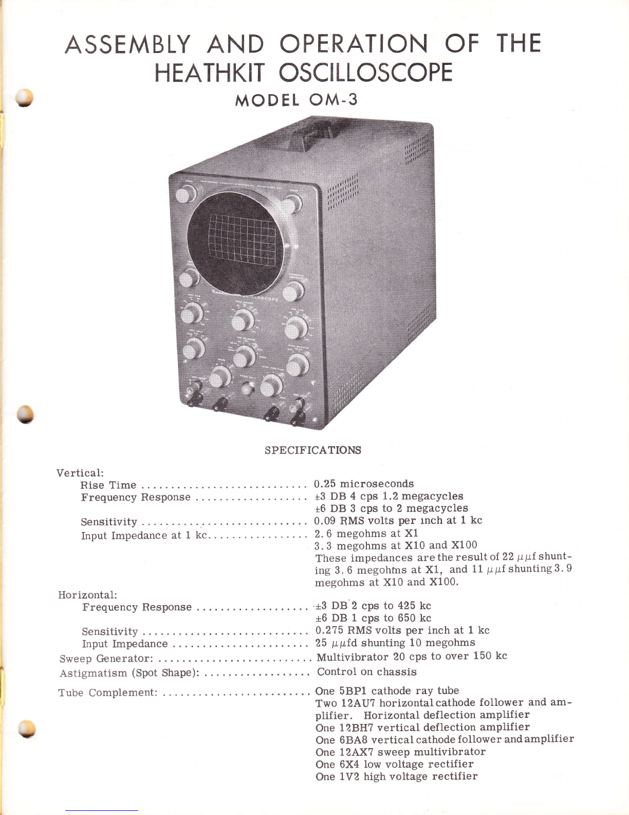
Power Requirements:.. ...105-125 volts AC, 5A/6C cycles, 65 watts
Dimensions:.... ... I 5/8" wide xr4lf9" high x lB" deep
Net Weight:. 18 lbs.
Shipping Weight:. ... 22 lbs.
INSTRUMENT DESCRIPTION
The Heathkit model OM-3 Oscilloscope is a relativelywide band, general purposeoscilloscope,
designed primarily for radio service, audio engineering, industrial electronics, production line
testing, amateur radio, and hobbyist, in fact, and application where a stable., sensitive oscil-
loscope is needed, but where the more expensive, broadband oscilloscope is not required.
Featuring a wide vertical response, down approximately 6 DB at 2 megacycles, and a modern
tube line-up, the model OM-3represents aconsiderable advantage in performance foran oscil-
Ioscope in this price range.
The cathode ray oscilloscope is, without a doubt, one of the most versatile electronic instru-
ments available today. It has earned this reputation because of its ability to display, in usable
form, the instantaneous relationshipsbetween anytwoelectrical quantities, no matterhow com-
plex, or between an electrical quantity and time. The oscilloscope can be used to evaluate dif -
ferentials in voltage, current flow, phase, frequency, waveform and time. With the unlimited
number of transducers available to the engineer today, it is a simple matter to convert any dy-
namic motion or static or dynamic physical quantity into an electrical signalwhich may then be
displayed upon the screen of the oscilloscope.
Probably the major use of most oscilloscopes is in the study of transient or recurrent electrical
phenomena" Since the oscilloscope is a voltage-operated device, these phenomena must first
be converted into voltage excursions.
In normal use, the signal to be observed is applied to the vertical input terminals of the oscil-
loscope. By means of attenuators and/or amplifiers this signal voltage is made to displace
vertically the electron beam in the cathode ray tube. Since, at the same time, the electron
beam is being displaced horizontallyand linearly with time bythe internal sweep generator, the
combined motion of the beam along both the X and Y axis traces out the instantaneous values of
the signal voltage with respect to time.
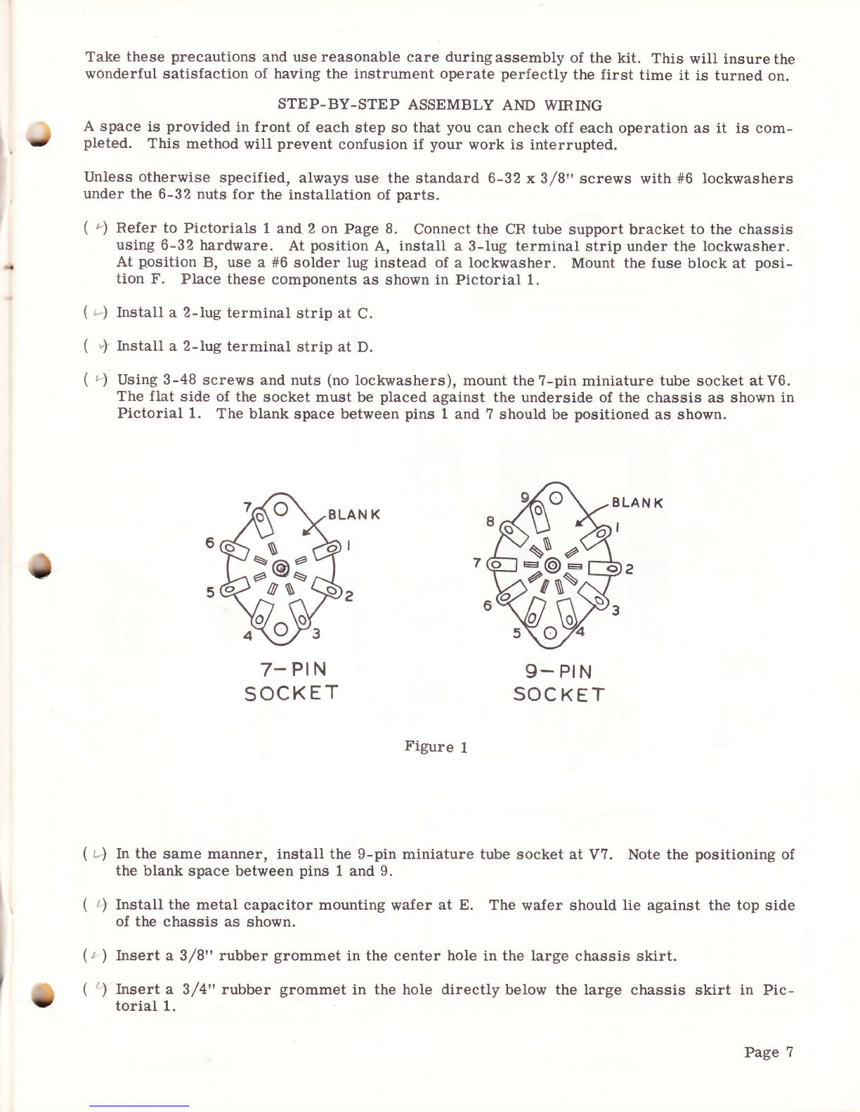
NOTES ON CMCUIT BOARD WIRING
hr line with the Heath Company's poticy of continualimprovementof its instruments, your Heath-
kit model OM-3.Oscilloscope utilizes circuit board, or "printed circuit" wiring. The Heath
Company was the first kit manufacturer to make use of this advanced technique i"n kit instru-
ments.
The process of etching, printing or silk screening a wiring pattern on a circuit board is not an
untried or experimental process. For years, one of the greatest hazards to quantity production
of electronic equipment has been the variable "stray" inductances and capacities caused by the
physicat plaeement of leads and components. Ir critical circuits, these variations become an
uncontrollable problem. During the first greatexpansion of televisionin the late 1940's, a tele-
vision tuner was developed using printed-circuit tuned circuits. It was so successful that the
technique was applied to millions of military electronic items where absolute uniformity, relia-
bility and low cost were paramount considerations. Today, the advantages of circuit board wir-
ing have made it an almost mandatory system for any commercial electronic mantrfacturer.
Since dip-soldering of manyconnections atone timereduceslabor cost, there is adecided econ-
omic advantage to the technique. In kit applications, dip-soldering is not practical of course.
But even more important is the absolute uniformity of each unit.
Page 3

.i It is this predictable uniformity that makes circuit-board wiring a major improvement in kit-
constructed electronic instruments. For the first time, you can be sure that your oscilloscope
will have the same characteristics as the development model. And, our engineers have been
able to incorporate refinements in circuitry which otherwise would have been entirely swamped
by the uncontrollable variables and strays introduced by conventional wiring.
HOW A CIRCUM BOARD IS PRODUCED
It is important to understand how a circuitboard is developed andmanufactured so that youmay
fully reilize its advantages. The board itself consists of alow-loss phenolic sheet' To one face
of tfiis sheet is bonded ilayer of pure metallic copper. This bonding process is the result of
years of research and developmentand has successfullypassed themost rigid militaryrequire-
ments for electronic equipment. The bond is not affected by moisture, aging, etching solutions
or normal variations in temperature.
The circuit pattern i.s developed after many experimental circuit layouts are tried and refined.
The circuit is finaily reduced to a drawing, bearing in mind necessary clearances for voltage
breakdown, capacity effects, elimination of undesired feedback possibilities and a minimum ol
cross-overs. The iinal drawing, enlarged severaltimes for greater accuracy, is photographed
and a negative of exact size is produced. The copper surface of the circuit board is sensitized
and expoied to light through the master negative. An etching process then removes aIIthe cop-
per exbept that piotected by the opaque areas of the negative. The result is a copper "print" of
the circuit pattern, as originaliy drawn.
Necessary holes are punched through the circuitboardand circuitcomponentsarethenmounted.
For physical supportj tttese parts ire generally mounted on the phenolic side of the board with
theif leads passed through holes and soldered directly to the pattern. Soldering is simple and
quick, using conventional methods.
One word of caution; we recommend that a small iron be used for circuit board soldering- The
amount of lreat required is much less than used for conventional wiring. Soldering pencils are
ideai; a 25 or 50 watt iron is entirely adequate. Soldering guns should be used carefully, since
they produce heat in direct ratio to length of time the switch is closed. Overheating can damage
the circuit board and should be avoided. It is not necessary to "sweat" the connections. Any of
the radio grades of solder work very well. DO NOT USE SOLDER PASTES OR OTIIER EX-
TERNAL FLLIXES, as they will completely ruin the circuit board.
GENERAL NOTES
UNPACK THE KIT CAREFULLY AND CHECK EACH PART AGAINST THE PARTS LIST. IN
so doing, you will become acquainted with the parts involved. Refer to the charts shown on the
inside couers of the manual to hetp you identify any doubtful components. If some shortage is
found in checking, please notify us promptly and return the inspection slip with your letter.
Hardware items are counted by-weight and if a few are missing, please obtainthem locally if at
all possible.
In order to expedite delivery to you, we are occasionally forced to make minor substitutions of
parts. Such substitutions are carefully checked before they are approved and the parts supplied
will work satisfactorily. By checking the parts list for resistors, for example, you may find
that a 2.2 megohm resistor has been Jupplied in place of. a 2 megohm as shown in the parts list'
These changes are self -evidentand are mentionedhere onlyto prevent confusionto youincheck-
ing the contents of your kit.
We strongly urge that You
of wires and parts is quite
acteristics of the circuit.
follow the wiring and parts layout shown in this manual. The position
critical inthis instrument and changes may seriouslyaffect the char-
Page 4

NOTES ON ASSEMBLY AND WIRING
The Heathkit Oscilloscope model OM-3 when constructed and used in accordance with the in-
structions in this manual, is a high quality instrument capable of rnany years of trouble-free
service. Therefore, we urge you to assemble the kit carefully. Do not hurry the work and you
will be rewardedwith a greatersense of confidence in yourability and in yournewOscilloscope.
This manual is supplied to assist and guide you in every way possible to complete the kit with a
minimum possibility of error. Each component has been identified pictorially andcolorcodes
and numerical values are specified each time a coded component is to be used. Elaborate pic-
torial diagrams and "step-by-step"wiring instructionsare included to help you construct your
kit with the greatest facility.
We suggest that you take a few minutes now and read the entire manual through before any work
is started. This wiil enable you to proceedwith thework much more rapidly when construction
is begun. The large fold-in pictorials are handy to attach to the waII above your work space
and their use will greatlysimplifyconstruction of this kit. These diagramsare also reproduced
in smaller size withinthe manual. We suggest thatyou retain themanual in yourfiles for future
reference, both in the use of the oscilloscope and for its maintenance.
Read the notes on soldering below. Crimp all leads tightly to the terminal before soldering.
Be sure that both the lead and terminalare free of wax, corrosion or other foreign matter. Use
only the best rosin core solder, preferably a type containing the new activated fluxes such as
Kester "Radio-TV Solder, " Ersin "Multicore" or similar types.
Resistors and controlsgenerallyhave a tolerance of *10%unless otherwisespecified in theparts
list. Therefore, a 100 Kfl control may test anywhere between g0 KO and 110 Kf,). (The letter
K is commonly used to designate a multiptier of 1000. ) Tolerance on capacitors are generally
even greater. Limits of +100% and -5070 are common for some types. The components fur-
nished with your Heathkit have been specified to enable you to obtain maximum performance,
accuracy and life from the completed instrument.
PROPER SOLDERING PROCEDI]RE
OnIy a small percentage of Heathkit purchasers find it necessary to return an instrument for
factory service. Of these, by far the largest proportion function improperly due to poor or
improper soldering.
Correct soldering technique is extremely important" Good solder joints are essential if the
performance engineered into the kit is to be fully realized. ff you are a beginner with no ex-
perience in soldering, a half-hour's practice with odd lengths of wire and a tube socket will be
a worthwhile investment.
High quality solder of the proper grade is most important. There are several different brands
of solder on the market, each clearly marked "Rosin Core Radio Solder. " Such solders consist
ofran alloyof tin and lead, usually in the proportion of 50:50. Minor variations.exist in the mix-
ture such as 40:60, 45:55, etc. with the first figure indicating the tin content. Radiosolders are
formed with one or more tubular holes through the center. These holes are filled with a rosin
compound which acts as a fltx or cleaning agent during the soldering operation.
NO SEPARATE FLIIX OR PASTE OF AI{Y KIND SHOULD BE USED. We specifically caution
against the use of so-called "non-corrosive" pastes. Such compounds, although not corrosive
at room temperatures, will form residues when heated. The residue is deposited on surround-
ing surfaces and attracts moisture. The resulting compound is not only corrosive but actually
destroys the insulation value of non-conductors. Dust and dirt wiII tend to accumulate on these
"bridEes" and eventually will create erratic or degraded performance of the instrument.
Page 5

I
,h
If terminals arebright and cleanand wires free of wax, frayed insulation andother foreign sub-
stances, no difficulty wili be experienced in soldering.'C"ii"p or otherwi?:j:::::":1""ntff"H:
;'r*:j'j"'ffil;ffiit,:;; JJ,Jilll* is made witho't relying on solder ror ptrvsical strength'
Topnake a goodsotrder joint, the cteantip of the soldering irorishouldbeplaced against the ioint
to be soldered so that the terminat is ieated sufficie"ify to melt solde'r. The solder is then
placed against both the terminal" and the tip of the iron and will lmmediately flow out over the
joint. Refer to the sketch below. use only enough solder to cover wires at the junction; it is
nct necessary to fiu the entire hole in the ierminit wi*r solder. Excess solder rnay flow into
tube socket contacts, ruining the socket, or it may creep into switch contacts and destroy their
spring action. posiiion the work "o in"i gravity iends tb t<eep the soLder where you want it'
A poor solder joint will usually be indicated by its appearance'
The solder will stand up in a blob on top of the connection,
with no evidence of flowlng out caused by actual' "wetting" of
the contact. A crystalline or grainy texture on the-solder
surface,causedbymovementofthejointbeforeit.solidified
is another evidence of a "cold" connection. In either event'
reheat the joint until the solder flows smoothly over the en-
lire junctidn, coolingto a smooth, bri'ghtappearance.' Photo-
S""ptt* in the adjoining picture clearly indicate these two
characteristics.
A good, clean, well-tinned soldering iron is also important to obtain consistently perfect con-
nections. For most wiring, a 60 or-100 watt iron, or the equivalent in a soldering gun, is very
satisfactory. smalrer irons generarly wiII not heat the connections enough to flow the solder
smoothly over the ioint and """ """o*mended only for light work, such as on etched circuit
boards, etc. Keep the iron tip clean and bright. A pad oisteel wool may be used to wipe the
tip occasionallY during use.
Page 6

J
Take these precautions and use reasonable care during assembly of the kit. This will insure the
wonderful satisfaction of having the instrument operate perfectly the first time it is turned on.
STEP.BY-STEP ASSEMBLY AND WIRING
A space is provided in front of each step so that you can check off each operation as it is com-
pleted. This method will prevent confusion if your work is interrupted.
Unless otherwise specified, always use the standard 6-32 x 3/8" screws with #6 lockwashers
under the 6-32 nuts for the installation of parts.
( a) Refer to Pictorials 1 and 2 on Page g. Connect the Cn tube support bracket to the chassis
using 6-32 hardware. At position A, install a 3-lug terminal strip under the lockwasher.
At ppsition B, use a #6 solder lug instead of a lockwasher. Mount the fuse block at posi-
tion F. Place these components as shown in Pictorial 1.
( *) Install a Z-lug terminal strip at C.
( ") [rstall a 2-Iug terminal strip at D.
( ,) Using 3-48 screws and nuts (no lockwashers), mount the?-pin miniature tube socket atV6.
The flat side of the socket must be placed against the underside of the chassis as shown in
Pictorial 1. The blank space between pins 1 and 7 should be positioned as shown.
BLAN K
BLAN K
I
7-PIN
SOCK E T9-PIN
SOCKET
Figure 1
( r-)
( ')
( r-)
( u)
In the same manner, install the 9-pin miniature tube socket at V7. Note the positioning of
the blank spaee between pins I and 9.
InstaII the metal capacitor mounting wafer at E. The wafer should lie against the top side
of the chassis as shown.
Insert a 3/8" rubber grommet in the center hole in the large chassis skirt.
Insert a 3/4" rubber grommet in the hole directly below the large chassis skirt in Pic-
torial 1.
>b<
as
%rt r
r\J t
pFs
q,g,
Page ?

o
PICTORIAL 1PICTORIAL 2

( "J From the top side ofthe chassis, insert the
electrolytic filter capacitor 25-32, into the
capacitor mounting wafer at E. Carefully
identify the four inner lugs and position them
as shown. While holding the capacitor firmly
in place, twist each of the four mounting
prongs about 1/8"turn. This willsecure the
filter capacitor in place.
( r) Mount a 2-lug terminal strip at AE, using 6-32 hardware.
(-) Mount a 1-lug terminal stripat AD, using 6-32 hardware.
( ,l"Mount the 1 megohmastigmatism control at AF, using acontrol
Solder AF1 to the control solder lug.
TWISTE O
MOU NTI NG
CONDENSER LUG MARKIN6S
Figure 2
solder lug and control nut.
N I CKEt
WASHER
C O NTROL
NUT
C ONTROL
SOLDER LUG
@(+
HOIV TO MOIJNT CONTROLS
USING A CONTROL SOLDER LUG Figure 3
(w) Examine thepower transformerandidentify ll
the color-coded wires coming out on either ll
side. Install the transformer using 8-32 ,A{l
hardware. AII white and black leads shouro ,,'1" ll
come out near the 9-pin socket. ll
It
( r) Referring toPictorial 2andFigure4, mount li
the 4-1ug terminal stripon the CR tubesup- ll
port bracket at G. Be sure to include one
of the small angle brackets, and use two
Iockwashers as shown. Figure 4
( ")' In the samemanner, installa 3-Iugterminal
strip and the other angle bracket at H.
( iC' Now insert 3/B"rubbergrommets inthetwo
3/8" holes in the CR tube support bracket.
AII wire referred to is insulated hookup wire unless otherwise specified. The ends should be
stripped of insulation about l/4". (S) means to solder the terminal immediately, making sure
that the solder contacts aII wires connected to that terminal. (NS) means do not solder yet be-
cause other connections are to be made to that terminal
1t') At the low voltage filter capacitor E, solder any one of the four twisted mounting prongs
to the metal capacitor mounting wafer. This will maintain a good ground connection for
the filter circuit.
,@
ERACKET
AN GL E'
BRACKET
TERM I NAL
STRIP
Page 9

( l' ) Connect a wire frorri lug E. (NS) to V6-7 (S).
NOTE: All resistors have a1/2 watt rating unless otherwise specified. They are the smallest
size with a body length of.3/8" and a diameter of. t/8". 1 wattresistors are 9/t6" long and have
a diameter of 7/32". 2 watt resistors are about Lt/16" long and have a diameter of 5/16". Be
sure to use the correct size in each position. Unless otherwise stated, disregard the "outside
foil" markings on tubular capacitors.
( ') Connect a 47 KO 2 watt resistor (yeliow-violet-orange) from E- (NS) to E- (NS).
(-') Connect a 4.7 KQ 2 watt resistor (yellow-violet-red) from E- (NS) to Er (NS).
( -) Now connect a 15 KQ 2 watt resistor (brown-green-orange) from E. (NS) to Er (NS).
( " ) Connect a wire from V6-4 (NS) to C2 (NS).
( r ) Connect a .005 prfd 1600 voit DC disc capacitor to V6-2 (NS). Wire the other lead to V6-6
(NS).
( r) Connect the red-yellow lead coming out of the power transformer to C2 (NS).
(Q Twist the two red transformerleads together andconnect either one toV6-1 (NS). Wirethe
other red lead to pin 6 (S) of the same socket.
I "') twist the two green transformer leads together and connect either one to V6-3 (NS). Con-
nect the other green lead to V6-4 (S).
(, ) Twist the twowhite leads together and connect either one to V7-5 (S). Wire the other white
lead to pin 4 (S) of the same socket.
( ") Twist the black leads together and dressthem alongtheside of the chassis as shown. Con-
nect either black lead to A2 (NS). Wire the other black lead to A3 (NS).
(t-.J Twist the two brown leads together and dress them along the chassis. Run the brown leads
through the large 3/4" grommet near the chassis skirt. Connect either brown lead to G4
(NS) on the CR tube support bracket. The other brown lead is then wired to G3 (NS).
(r ) Identify the cable assembly consisting of color-coded wires. At one end there will be only
four free wires colored orange, red, yellow and blue. Insert this end of the cable through
the large 3/4,, grommet from theunderside of the chassis" Thesecabled wires are already
cut to proper tength and stripped. On the CR tube support bracket, connect the yellow wire
to G3 (NS). See Pictorial 4.
( t ) Connect the red wire to G2 (NS).
( . ) Connect the blue wire to H2 (NS).
( " ) Connect the orange wire to H1 (NS).
( r.) On the underside of the chassis, dress the cable down the chassis edge.
(;, ) Coming out of the cabie will be two white, an orange and two red leads. Connect either
white lead to A1 (NS).
( .) Connect the other white lead to A3 (S).
( 1.) Dress both of the red leads between socket V7 and terminal strip D as shown. Connect
' both re]I-leads to D2 (NS).
Page 10

a
o
o
4 CABLED WIRES
ED_ ORANGE -YELLOW_ BLU E
PICTORIAL 3Page 11

(\4
1 tu) Connect the orange lead to AF2 (S).
( t) select the line cord and tin each lead end to hold the copper strands together and make sol-
dering easier.
Insert the line cord into the chassis through the 3/8" rubber grommet in the chassisskirt'
Tie a knot in the cord about 6" from the end for strain relief. Connect either lead to A1
(S). Wire the other lead to F2 (S).
Connect a wire from Er (NS) to AF3 (S).
Connect a wire from A2 (S) to F1 (S).
Position the .1 pfd 1600volt DC paper tubular capacitor as shown and connect one lead to
solder lug B (NS). Pass the other lead through Dl (NS) to V?-9 (S) (use sleeving)'
In the same manner, connect either lead of the .2 pfd 1200 volt DC papertubular capacitor
to solder lug B (S). Wire the other lead to D2 (NS)'
(")
(u4
( r")
\ /.)
(
(
,-),'Now connect a 100 KQ resistor (brown-black-yellow) from Dl (S) to D2 (S)'
r,) Lay aside the chassis for the time being and set up the "direct input bracket" as shown'
Insiall the DpDT slide switch sw, using 6-32 hardware.
Figure 5Figure 6
(l)Nowinstailthe2.screwterminalstripJfromtheoppositesideofthebracketsothatthe
lugs extend through the bracket hole'
(uz)Connecta.00sg,fddisccapacitorfromsw6(s)toJ1(S).Dressasshown.
(r,,) Connect another .005 prfd disc capacitor from SW3 (S) to J2 (S) (use sieeving)'
( r,) wire a I megohm resistor (brown-black-green) from sw1 (NS) to sw2 (NS)'
(t)ConnectanotherlmegohmresistorfromsW4(NS)toSw5(NS).
Page 12
eNo
-61----ar-----
g/ \;/
BRAC K ET
DIRECT INPUT
BRACKET
4

( Lf Connect one end of a12 L/2" piece of wire to SW1 (S). Leave the other end free.
(e,) Connect one end of aL2 l/2" piece of wire to SW4 (S). Leave the other end free.
( e'.) Connect a 4" piece of wire to SW2 (S). Leave the other end free.
( r') Connect a 4" piece of wire to SWb (S). Leave the other end free.
( :') The long leads attached to lugs 1 and 4 of switch SW can now be inserted through the 3/8"
grommet near terminal strip H on the CR tube bracket as shown. Now install the direct
input bracket on the CR tube bracket using 6-32 hardware.
( ') Connect the free end of the lead from SW2 to pin 9 (S) of the ll-pin CRT socket. Refer to
Pictorial 4 for proper positioning.
(r') Connect the short leadfrom SW5 to pin 6 (S) of the CRT socket.
({ Connect one end of a L6 1/2" piece of wireto H3 (NS). Pass the other end of thewire under
the colored cable wires and run it through the 3/B"grommet locatednear terminalstrip G.
Leave this end free.
(,1') Now connect one end of a 14" piece of wire to G1 (NS). hrsert the other end through the
same grommet near G and leave this end free.
( i ) Cut and strip both ends of seven pieces of wire, each of which should be 4" Iong. Connect
the first wire from Gl (S) to pin B (S) of the CRT socket.
( ,,.) Connect the second wire from G2 (S) to pin 10 (S) of the CRT socket.
TO SW-2
TO Sw-5
INSERT WIRES
FROM SW I AND
4 HERE
BLUE
ORANGE
CRT SUPPORT BRACKET
PICTORIAL 4
i^9e\'
'9o- 6 i9
e'O!f
Page 13

o
z
INTEN
VE RT. CENT.
a
HOR. GAIN
VERT. GAI N
I
3
4
PHASE VERT. INPUT
SYNC. SELECTOR ,^a/-\
,w
' s'.W"i,l'
sL5
"-re) r'.reDEXr.sYNc. IV P-P
SL6
@.,
FOCUS
VERNIER
SYNC. AMP.
@sL3
{
I
I
I
I
I
I
I
I
i
I
I
I
I
tI
I
t
Page 14
PICTORIAL 5

( lc) ffre third wire shoutrd now be connected from G3 (S) to pin 11 (S) of the CRT socket.
( t"J Connect the fourth wire from G4 (S) to pin 1 (S) of the CRT socket.
( 9-'Connect the fifth wire from H2 (S) to pin 4 (S) of the CRT socket.
( &f Connect the sixth wire from H3 (S) to pin 3 (S) of the CRT socket.
(&")rConnect the seventh wire from H1 (S) to pin ? (S) of the CRT socket.
NOTE: When installing controls and switches, flatten out any locating prong that might inter-
fere with a secure mounting to the panel.
( u) Refer to Pictorial 5 on Page 14 and begin the assembly of the parts to the front panel. In-
stall the 500 KA FOCUS control at K. Use a control solder lug instead of a control lock-
washer. Position the lugs as shown.
C ONTROL
NUl
A
w
Figure 7
( ;)
( i') Using a control solder lug, mount the 20 KO HOR.
soider lug back to contact lug 3 and solder.
HOW TO. MOUNT CONTROLS & SWITCHES
GAIN control at O. Bend the control
1 v)' Use another control solder lug and install the 7500 KO FREQ. VERNIER control at P. Bend
back the control solder lug and solder it to lug 2 of the control.
(r ) Install the 10 K(-) VERT. GAIN control atQ, using a control solder lug, flat washerand nut.
(/) lnstatl one of the 3-position rotary switches 63-4? at position R. Orient the lugs asshown.
(,") Simiiarly, mount the other 3-position switch at T.
( ) Now install the 6-position rotary switch 63-83 at position S. Before tightening the control
nut, rotate the switch so that lugs 9 and 10 are closest to the FREQ. VERNIER control P.
( ,I Now instail the 50 KO INTEN. control at L.
Notice that this control has two extra lugs
at the rear and one extra on the side.
Installthe 50 Kfl HORIZONTAL CENTERING
control at M.
Install the 50 Kf) VERTICAL CENTERING
controi at N.
( r"-) Refer to Figure 8 and mount the pitot light
assembly at PL. The bushing, Iamp and
jewel are installed from the front of the
panel.
1z) Now install the 1 megohm SYNC. AMPLI-
TUDE control at U. Use a control solder
Iug, and solder it to U3.
( { tnstatl the ?500 KO PHASE control at V.
PANEL
C ONTROT
LOCKWASH ER
(r)
@6
Figure I
PlLor LIGHr ASSEMgLY Page 15

o
20K
680K
lw
,u!ou{c t
._wsL5 SL6
".r@
I
L
l-
Page 16
PICTORIAL 6

{ a"f Install binding post bases in each of the six
holes at the bottom of the panel. Refer to
Figure 9 anduse theinsulator bushingswith
a #6 solder lug under the nut. Position the
solder lugs as shown in Pictorial 5 at posi-
tions SL1, SLz, SL3, SL4, SL5 and SL6.
('4 Mount the CR tube ring as shown. The
' mounting brackets should rest against the
inside surface of the panel and the seam in
the ring should be downward. Secure with
\,n"utoaoR BUsHTNGs
^:;;*';:,'"" ;l-'
s HolN
A
(a-op)
\y
Figure 9
#6 sheet metal screws.
(v) Connecta22A KQ resistor (red-red-yellow) from L3 (S) to Il (NS). Dressas shown inPic-
torial 6.
( ,f Connect a 680 KO 1 watt resistor (blue-gray-yellow) from K3 (S) to the control solder lug
(S) at K.
(-') Connect a 47A KO resistor (yellow-violet-yellow) from Pl (S) to S12 (S).
(rJ Connect either lead of a .1 pfd 400 volt DC capacitor to U1 (S) (use sleeving). Dress the
capacitor as shown and connect its other lead to R4 (S).
( r) Connect a wire from R3 (S) to solder lug SLZ (S).
( -1' Connect a wire from R2 (NS) to PL1 (NS).
( i..) Connect a 100 trrpf disc type capacitor from sG (S) to 55 (NS).
( uJ Connect a .001 prfd disc type capacitor from 55 (S) to 54 (NS).
(,,) Connect a.01 pfd disc type capacitor from 54 (S) to 53 (NS).
( l,') Connect either lead of a .1 pfd 200 volt DC capacitor to the control solder tug (NS) under
the SYNC. AMPLITITDE control U. Connect the other lead to S3 (S).
( .,) Connect a 150 KQ resistor (brown-green-yellow) from the same control solder lug (S) at U
to 52 (NS).
( v) Connect a 10 rnegohm resistor (brown-black-blue) from 52 (S) to V3 (NS) (use sleeving).
( '") Connect a wire from 51 (S) to the solder lug SLl (S).
( t ) Connect a l KOresistor (brown-black-red) from solderlug SL3 (NS) to PL1 (S) (use sleev-
ing).
( ,4 Connect a 62 Q 5ft resistor (blue-red-black-gold) from SL3 (S) to PL2 (NS).
( ,') Remove the insulation f rom a short piece of wire and connect PLZ (S). Solder the other end
of the frame of the pilot light socket as shown.
( i.J Now connect a wire from solder lug SL4 (NS) to T4 (S).
.<
Y,)
&.
\P)
Page 17

CIRCUIT BOARD ASSEMBLY
The values and locations of alL components to be mounted on the circuit board are printed on the
board itself for your convenience" To anyone experienced in this relativelynew wiring method,
this inforrnation will be self-expianatory. AII parts, including five 9-pin sockets, are inserted
into the board from the printedliae. They are'then soldered io the etched side of the board and
resistor and capacitor llads are then ctipped to a length of about L/8". Of course, the sockets
rnust be rotated until the blank space between pins 1 ind I correspond to the blank space in the
metal circuit Pattern. .,
The foliowing method of construction hasbeen found to bemostpracticaland it is suggested that
you proceed in this sequence.
First select thetwenty-three L/2 watt resistor
values to be installed on the circuit board and
bend each lead to a 90o angle as close as pos-
sible to the resistor body. The values are as
follows:
2 - 2.2 megohm (red-red-green)
3 - 2.2 KQ (red-red-red)
3 - 47 KO (yellow-violet-orange)
2 - 100 KO (brown-btack-Yellow)
L - 270 O (red-violet-brown)
2 - 470 KO (yellow-violet-Ye1iow)
4 - 10 KQ (brown-black-orange)
I - L"2 KQ (brown-red-red)
L - 22 KQ (red-red-orange)
t - 3.3 KQ (orange-orange-red)
1 - I megohm (brown-black-green)
1 - 3.9 KO (orange-white-red)
1 - 10 megohm (brown-biack-blue)
SOCKTT LUGS
BENT OVER ENOUG}I TO
HOLD SOCKET TO BOARD
*,p8-.,il.-.? 3- os
,6 l"s 9;J
dE \;q.o^:^_."1c:;_",y,,,,
'?Pt+;;ix, : NN
lt -". ?. : :; . :^"
tl-"n 2\| '. -k
"-t q* 6^" c
?1" o- .? [o^ " - ?$
.ri*--- ""3i * **t '{.'8
QG,ili,, G--
i* $r.sx t
,'?
5ta
,t!
""f
t"
e
2.2
oI'
r-t c
':r;l
l}toox-
ti
ol /a
t2^v7 /
-1\ a
?\
tr
r?
o?'t
a/
orr/*
\.
?\
tr
r?
o9'l
.ii.
?\
i,.^
t:
Ii
?
oo
Install each resistor from the phenolic side of the board as shown' Ir{ake sure that the correct
value is used in each position. presseach resistorin place until it liesagainst the-circuitboard
itself. Turn the board over and solder each resistor lead to the metal surrounding the hoie
throughwhich the lead protrudes. A smalltippedironwith arating of 25 wattsto 50watts should
be used if possible. Soldering pencils ane eiceitent. If a soldering gun is used, do not touch
the tip to tle circuit board until it is hot enough to solder immediately'
| 6-+o'*-3 .a 6
l+-
L
Figure 11
as youcan around the edges of
leads can be reached. In this
O4\ ] C,RCUI' BOARD SCFEFN
Figure tr 0
LEADS SPREAO
AFTER INSERTIOI-i IN I'lOLE
the board. These
way, you will soon
FOIL
CIRCUIT
ON THIS SIDE
OF EOARD
C OMPONE NT
f{ARXtNGS oN THlS
SIDE OF BOARD
SOEKET
MOUN T I NG
A convenient method is to solder as many leads
leads can 'hen be clippedoff short sothat more
have aII 23 resistors soldered in place'
Page 18'

,
,o
Proceed in the same manner to install and solder the following parts:
2 - I5 KQ 2 watt resistors (brown-green-orange)
2 - 47 KO 1 watt resistors (yellow-violet-orange)
1 - .001 trrfd disc capacitor
3 - .02 pfd disc capacitor
1 - .0025 pfd disc capa"citor
1 - .1 pfd 200 volt DC tubular capacitor
1 - 10 KQ 2 watt resistor (brown-black-orange)
NOTE: The 10 K 2 watt resistor should be spaced approximately 3/8" above the surface of the
circuit board. The mounting holes have purposelybeen placed close together to prevent seating
this resistor against the circuit board.
47 K-tW
-n-D 3.9K
fi@'e-
ffin
2A
ro K
I.OM
.fl-IITIIhE
3.3 K
12 AX7 47K 2AU7
toK 2w
&6,,"
2.2R
o47K
t5 K-2W
toK too K
@
oeA* 2''M
W 4l'rTlIl'T\-
" 47K
PICTORIAL 7
Before installing the sockets, each one should be "broken in" by inserting any 9-pin miniature
tube several times. This will loosenup thepins andpreventpossibledamage to thecircuit board
through the use of heavy pressure when tubes are permanently installed.
1 l"i Now install the five 9-pin miniature tube sockets from the component side of the board.
Rotate each one for proper orientation of the blank space between pins 1 and 9. Bend each
pin (except pin B of V1, pins 3 and B of V2 and V5 and pins 1 and ? of V3) flat against its
corresponding metal circuit pattern connection. Now solder the bent pins to the pattern.
m,,
Page 1.9
Table of contents
Other Heathkit Test Equipment manuals