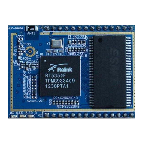
Hi-Link WM7628N-A User manual

2
CONTENTS
1.1. BASIC PARAMETER........................................................................................................................................ 10
2.
DIAGRAM.................................................................................................................................................................11
3.
ELECTRICAL CHARACTERISTIC............................................................................................................................ 12
3.1. POWER SUPPLY REQUIREMENT...................................................................................................................... 12
3.2. RF PERFORMANCE...........................................................................................................................................12
802.11B11M.....................................................................................................................................................12
802.11G54M.....................................................................................................................................................13
802.11NMCS7(HT20).......................................................................................................................................13
802.11N_MCS7(HT40).......................................................................................................................................14
4.
MODULE PINS DEFINITION.................................................................................................................................. 14
4.1. DEFAULT PIN DEFINITION CHART.............................................................................................................. 14
5.
MODULE DIMENSION CHART.................................................................................................................................. 17
6.
EUROPEAN LABEL...................................................................................................................................................18

10
1.
INTRODUCTION
WM7628N-A based on MT7628NN is a low cost and low power consumption IOT module
developed. This module leads to all the interfaces of MT7628NN,The module supports Linux,
OpenWRT operating system and custom development. It could be widely applied to smart devices
or cloud services application with its rich interface and powerful processors, at the same time ,it
also support secondary development.
1.1. BASIC PARAMETER
High data processing ability,MCU frequency 580MHz
300M Mbps
Support 802.11b/g/n
20/40 Channel bandwidth
Support 802.11v
Support AP,STA and AP,STA mixed
Five 10/100M ETH PORT
1 USB2.0 Host interface port
Interface SPI/SD-XC/eMMC
Rich peripheral interfaces,SPI,I2C,I2S,PCM,UART,JTAG,GPIO
Widely used in IOT
Inbuilt powerful PMU
Support 16 Multiple BSSID
Support multiple security methods WEP64/128, TKIP,AES, WPA, WPA2, WAPI
Support QoS,WMM,WMM-PS
Support Linux 2.6.36 SDK,OpenWrt 3.10

11
2.
DIAGRAM
WM7628N-A Module architecture diagram
2.1. SPECIFICATIONS
Item
Parameter
Note
Model
WM7628N-A
Version V1.0
Chip
MT7628AN/MT7628NN
Kernel
MIPS24KEc
Basic frequency
580MHz
RAM
DDR2 128MB
Customizable DDR2
64M/32MB
Flash
32MB
Customizable 16MB/8MB
Temperature
Environment temperature:-40℃~85℃
Humidity
Working:10~95%(noncondensing)
Storage:5~95%(noncondensing)
EINT
Ethernet
UART
GPIO
PWM
USB_HOST
SPI
SPIS
I2C
I2S
JTAG
SDXC
MT7628AN
/MT7628NN
3.3V
40MHz
DDR2(1Gbit/128Mbit)
SPI Flash(256Mbit/128Mbit)
IPEX Connector

12
Size
18mm×35.2mm×2.8mm
2.2. INTERFACE NUMBER
Interface
Contain interface
Interface supported
WiFi Standard
IEEE 802.11b/g/n
Support
Ethernet Interface
Five 10/100M ETH PORT
1 WAN、4 LAN
UART
3
2 UART support transmitting
SDIO
1
Non support
SPI
1
Non support
I2C
1
Non support
I2S
1
Non support
PWM
1
Non support
GPIO
More than
8
Defined functions
Notes: 1、The module was
default embedded our firmware which based on Linux; the Ethernet,WiFi,UART0 and UART1 of the firmware have
the function of transmission
2、Based on actual usage, the module also can be embedded OPENWRT program and LINUX program of MTK original
plant before sent out.
3.
ELECTRICAL CHARACTERISTIC
3.1. POWER SUPPLY REQUIREMENT
Power supply requirement
Input voltage
DC:3.3±0.2V
Non-load current
170±50mA
Supply current
≥800mA
3.2. RF PERFORMANCE
802.11b 11M
802.11b Transmit (Conductive)
Item
Condition
Min.
Typ.
Max.
Unit
Frequency Range
Channel 1
Channel 13

13
Tx Power Level
DQPSK
18
20
22
dBm
Frequency Tolerance
-15
0
15
ppm
Spectral Mask
11MHz→22MHz
40
dBr
>22MHz
53
dBr
Modulation Accuracy
All Data Rate
15
%
802.11b Receiver (Conductive)
Item
Condition
Min.
Typ.
Max.
Unit
Frequency Range
Channel 1
Channel 13
Min. Input
11Mbps PER<8%
-91.5
-89.5
-87.5
dBm
802.11g 54M
802.11g Transmit (Conductive)
Item
Condition
Min.
Typ.
Max.
Unit
Frequency Range
Channel 1
Channel 13
Tx Power Level
OFDM
15
17
19
dBm
Frequency Tolerance
-15
0
15
ppm
Modulation Accuracy
All Data Rate
-31
-28
%
802.11g Receiver (Conductive)
Item
Condition
Min.
Typ.
Max.
Unit
Frequency Range
Channel 1
Channel 13
Min. Input
54Mbps PER<10%
-78.0
-76.0
-74.0
dBm
802.11n MCS7(HT20)
802.11n_HT20 Transmit (Conductive)
Item
Condition
Min.
Typ.
Max.
Unit
Frequency Range
Channel 1
Channel 13
Tx Power Level
OFDM
15
17
19
dBm

14
Frequency Tolerance
-15
0
15
ppm
Modulation Accuracy
All Data Rate
-31
-28
dB
802.11n_HT20 Receiver (Conductive)
Item
Condition
Min.
Typ.
Max.
Unit
Frequency Range
Channel 1
Channel 13
Min. Input
MCS7 PER<10%
-76.5
-74.5
-72.5
dBm
802.11n_MCS7(HT40)
802.11n_HT40 Transmit (Conductive)
Item
Condition
Min.
Typ.
Max.
Unit
Frequency Range
Channel 1
Channel 13
Tx Power Level
OFDM
15.0
17.0
19.0
dBm
Frequency Tolerance
-15
0
15
ppm
Modulation Accuracy
All Data Rate
-31
-28
dB
802.11n_HT40 Receiver (Conductive)
Item
Condition
Min.
Typ.
Max.
Unit
Frequency Range
Channel 1
Channel 13
Min. Input
MCS7 PER<10%
-76.5
-74.5
-72.5
dBm
4.
MODULE PINS DEFINITION
4.1.DEFAULT PIN DEFINITION CHART
PIN
Name(Function 1)
Function 2
Function 3
Function 4
G
P
I
O
#
Note
1
GND
2
3
.
3
V
D
Supply current≥800mA
3
3
.
3
V
D
Supply current≥800mA
4
GND
15
5
S
P
I
_
C
S
0
G
P
I
O
#
10
S
P
I
bus chip select
0
6
REF_CLK0
G
P
I
O
#
38
Reference clock output
7
PERST_N
G
P
I
O
#
36
P
C
I
e
device reset
8
WDT_RST_N
G
P
I
O
#
37
Watchdog reset
9
EPHY_LED4
JTAG_RST_
N
G
P
I
O
#
39
10
EPHY_LED3
JTAG_CLK
G
P
I
O
#
40
11
EPHY_LED2
JTAG_TMS
G
P
I
O
#
41
12
EPHY_LED1
J
TA
G
_
T
D
I
G
P
I
O
#
42
13
EPHY_LED0
JTAG_TDO
G
P
I
O
#
43
14
PORST_N
CPU reset
15
UART_TXD1
PWM_CH0
G
P
I
O
#
45
Port 1 date transmission
16
UART_RXD1
PWM_CH1
G
P
I
O
#
46
Port 1 date reception
17
I
2
S
_
S
D
I
PCMDRX
G
P
I
O
#0
I
2
S
date input
18
I
2
S
_
S
D
O
PCMDTX
G
P
I
O
#1
I
2
S
date output
19
I
2
S
_
W
S
PCMCLK
G
P
I
O
#2
I
2
S
sound channel
selection
,
0
:
left
;
1
:
right
20
I
2
S
_
C
L
K
PCMFS
G
P
I
O
#
3
I
2
S
21
GND
22
ANT
Antennal RF interface(not
connect)
23
GND
24
I
2
C
_
S
C
L
K
G
P
I
O
#
4
I
2
C
25
I
2
C
_
S
D
G
P
I
O
#
5
I
2
C
26
S
P
I
_
C
S
1
G
P
I
O
#
6
SP 1
27
S
P
I
_
C
L
K
G
P
I
O
#
7
S
P
I
28
S
P
I
_
M
I
S
O
G
P
I
O
#
9
S
P
I
29
S
P
I
_
M
O
S
I
G
P
I
O
#
8
S
P
I
30
G
P
I
O
0
G
P
I
O
#
11
31
UART_TXD
0
G
P
I
O
#12
Port 0 date output
32
UART_RXD
0
G
P
I
O
#13
Port 0 date input
33
WLED_N
G
P
I
O
#44
W
i
F
i
L
E
D
34
M
D
I
_
R
P
_
P
0
35
M
D
I
_
R
N
_
P
0

16
36
M
D
I
_
T
P
_
P
0
37
M
D
I
_
T
N
_
P
0
38
M
D
I
_
T
P
_
P
1
S
P
I
S
_
C
S
PWM_CH0
G
P
I
O
#14
39
M
D
I
_
T
N
_
P
1
S
P
I
S
_
C
L
K
PWM_CH1
G
P
I
O
#15
40
M
D
I
_
R
P
_
P
1
S
P
I
S
_
M
I
S
O
UART_TXD
2
G
P
I
O
#16
41
M
D
I
_
R
N
_
P
1
S
P
I
_
M
O
S
I
UART_RXD
2
G
P
I
O
#17
42
M
D
I
_
R
P
_
P
2
eMMC_D7
PWM_CH0
G
P
I
O
#18
43
M
D
I
_
R
N
_
P
2
eMMC_D6
PWM_CH1
G
P
I
O
#19
44
M
D
I
_
T
P
_
P
2
UART_TXD2
eMMC_D5
PWM_CH2
G
P
I
O
#20
45
M
D
I
_
T
N
_
P
2
UART_RXD2
eMMC_D4
PWM_CH3
G
P
I
O
#21
46
M
D
I
_
T
P
_
P
3
SD_WP
eMMC_WP
G
P
I
O
#22
47
M
D
I
_
T
N
_
P
3
SD_CD
eMMC_CD
G
P
I
O
#23
48
M
D
I
_
R
P
_
P
3
SD_D1
eMMC_D1
G
P
I
O
#24
49
M
D
I
_
R
N
_
P
3
SD_D0
eMMC_D0
G
P
I
O
#25
50
M
D
I
_
R
P
_
P
4
SD_CLK
eMMC_CLK
G
P
I
O
#26
51
M
D
I
_
R
N
_
P
4
SD_CMD
eMMC_CMD
G
P
I
O
#28
52
M
D
I
_
T
P
_
P
4
SD_D3
eMMC_D3
G
P
I
O
#29
53
M
D
I
_
T
N
_
P
4
SD_D2
eMMC_D2
G
P
I
O
#27
54
USB_DP
55
USB_DM
56
GND
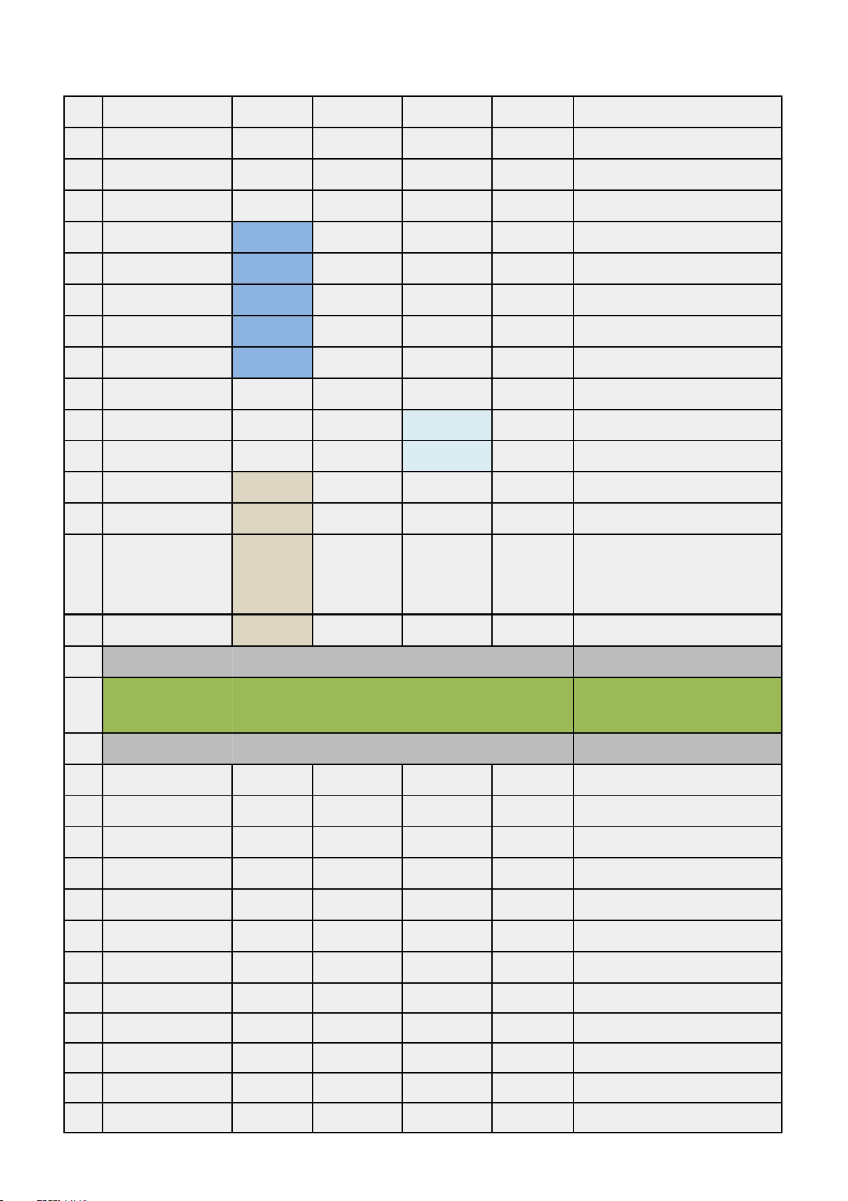
Notes:
1,All pins default 1,drive current 8MA.
2, Red representation on the name bar: related to the start of the chip, the outside can not be
pulled up and down, not connected with the driver source.
3,Blue representation on the name bar: The default firmware .
4,The module of MT7628NN chip does not have PCIE interface

17
5.
MODULE DIMENSION CHART
Module dimension chart (TOP)
Recommended package size diagram
Notes:
1,The three intermediate pads are hot pads, please ground.
2,Package pad epitaxial size can be appropriately shortened or lengthened according to demand.

19
FCC regulatory information
This device complies with Part 15 of the FCC Rules. Operation is subject to the following two
conditions: (1) this device may not cause harmful interference, and (2) this device must accept any
interference received, including interference that may cause undesired operation.
Warning: changes or modifications not expressly approved by the party responsible for compliance
could void the user’s authority to operate the equipment.
End Device Labelling
Please notice that if the FCC identification number is not visible when the module is installed
inside another device, then the outside of the device into which the module is installed must also
display a label referring to the enclosed module. This exterior label can use wording such as the
following: “Contains FCC ID: Z4T-WM7628N-A”any similar wording that expresses the same
meaning may be used.
RF Exposure Compliance
This equipment complies with FCC radiation exposure limits set forth for an uncontrolled
environment. This equipment should be installed and operated with a minimum distance of 20cm
between the radiator & your body. This transmitter must not be co-located or operating in
conjunction with any other antenna or transmitter.
Installation Notice
The module is limited to OEM installation ONLY. The OEM integrator is responsible for ensuring
that the end-user has no manual instruction to remove or install module.
The module is limited to installation in mobile application; A separate approval is required for all
other operating configurations, including portable configurations with respect to Part 2.1093 and
difference antenna configurations.
FCC Part 15B Compliance of End Device

20
The OEM integrator is responsible for ensuring that the host product which is installed and
operating with the module is in compliant with Part 15B unintentional Radiator requirements,
please note that For a Class B digital device or peripheral, the instructions furnished the user
manual of the end-user product shall include the following or similar statement, placed in a
prominent location in the text of the manual:
Note: This equipment has been tested and found to comply with the limits for a Class B digital
device, pursuant to part 15 of the FCC Rules. These limits are designed to provide reasonable
protection against harmful interference in a residential installation. This equipment generates, uses
and can radiate radio frequency energy and, if not installed and used in accordance with the
instructions, may cause harmful interference to radio communications. However, there is no
guarantee that interference will not occur in a particular installation. If this equipment does cause
harmful interference to radio or television reception, which can be determined by turning the
equipment off and on, the user is encouraged to try to correct the interference by one or more of the
following measures:
—Reorient or relocate the receiving antenna.
—Increase the separation between the equipment and receiver.
—Connect the equipment into an outlet on a circuit different from that to which the receiver is
connected.
—Consult the dealer or an experienced radio/TV technician for help.
OEM Installation Guidance Document
FCC ID: Z4T-WM7628N-A
Conditions on using Seeed regulatory approvals:
A. Customer must ensure that its product (the“CUSTOMER Product”) is electrically identical to
Seeed reference designs. Customer acknowledges that any modifications to Seeed reference designs
may invalidate regulatory approvals in relation to the CUSTOMER Product, or may necessitate
notifications to the relevant regulatory authorities.
B. Customer is responsible for ensuring that antennas used with the product are of the same type,
with same or lower gains as approved and providing antenna reports to Seeed.
C. Customer is responsible for regression testing to accommodate changes to Seeed reference
designs, new antennas, and portable RF exposure safety testing/approvals.
D. Appropriate labels must be affixed to the CUSTOMER Product that comply with applicable
regulations in all respects.

21
E. A user’s manual or instruction manual must be included with the customer product that contains
the text as required by applicable law. Without limitation of the foregoing, an example (for
illustration purposes only) of possible text to include is set forth below:
1. USA—Federal Communications Commission (FCC)
FCC COMPLIANCE STATEMENT:
This device complies with part 15 of the FCC Rules. Operation is subject to the following
two conditions:
(1) This device may not cause harmful interference, and (2) this device must accept any
interference received, including interference that may cause undesired operation.
INFORMATION TO USER:
2.1 General:
This equipment has been tested and found to comply with the limits for a Class B digital device,
pursuant to Part 15 of FCC Rules. These limits are designed to provide reasonable protection
against harmful interference in a residential installation. This equipment generates, uses, and can
radiate radio frequency energy. If not installed and used in accordance with the instructions, it may
cause harmful interference to radio communications. However, there is no guarantee that
interference will not occur in a particular installation. If this equipment does cause harmful
interference to radio or television reception, which can be determined by tuning the equipment off
and on, the user is encouraged to try and correct the interference by one or more of the following
measures:
-Reorient or relocate the receiving antenna
-Increase the distance between the equipment and the receiver.
-Connect the equipment to outlet on a circuit different from that to which the receiver is connected.
-Consult the dealer or an experienced radio/TV technician for help.
FCC Caution: Any changes or modifications not expressly approved by the party
responsible for compliance could void the user's authority to operate this equipment.
System integrators must include the FCC ID on the end product.
2.2 List of applicable FCC rules:
The Seeed module is only FCC authorized (certified) for the transmitterspecific rule parts, FCC
15.247. OEM manufacturer is responsible for compliance to all other FCC rules that apply to the
host.
2.3&2.6 Summarize the specific operational use conditions and FCC Radio-Frequency
Exposure & Approval Conditions:
Transmitting antenna(s) can only be installed at the display section of computer. When this device

22
is installed other than notebook computers, at least 20 cm separation distance shall be maintained
between the transmitting antenna(s) to the body of user or nearby person.
2.4 Limited module procedures:
The module is an unrestricted module
2.5 Trace antenna designs:
The antenna(s) used for this transmitter must not be collocated or operating in conjunction with any
other antenna or transmitter within a host device, except in accordance with FCC multi-transmitter
product procedures.
2.7 Antennas:
The module grantee is responsible for providing the documentation to the system integrator on
restrictions of use, for continuing compliance of the module including the maximum antenna gain
(6dBi), minimum antenna gain (3dBi), Antenna connector is a unique I-PEX connector.
2.8 Label and compliance information:
The regulatory label on the final system must include the statement: “Contains FCC
ID:Z4T-WM7628N-A”using electronic labeling method as documented in KDB 784748.
2.9 Information on test modes and additional testing requirements:
OEM manufacturer should perform additional verification/validation on supported modes and is
responsible for validation testing of module + host.
The final system integrator must ensure there is no instruction provided in the user manual or
customer documentation indicating how to install or remove the transmitter module except such
device has implemented two-ways authentication between moduleand the host system.
2.10 Additional testing, Part 15 Subpart B disclaimer:
This device complies with Part 15 of the FCC Rules. Operation is subject to the following
two conditions: (1) This device may not cause harmful interference, and (2) this device must accept
any interference received, including interference that may cause undesired operation.
FCC Caution: Any changes or modifications not expressly approved by the party
responsible for compliance could void the user's authority to operate this equipment.
7. It is forbidden to operate transmitters outside the 2.4-2.4835 GHz frequency band to control or
communicate
8. The certified WLAN module will be installed in mobile application.
9.This module is for integration into a host system which is intended.
Table of contents
Other Hi-Link Network Hardware manuals
Popular Network Hardware manuals by other brands
LG-Nortel
LG-Nortel ipLDK-60 installation manual
Matrix Switch Corporation
Matrix Switch Corporation MSC-HD161AAL product manual
Avigilon
Avigilon HD-NVR4-PRM-64TB user manual
Belkin
Belkin F1DU120 - Pulse Network Monitor Quick installation guide
Clavister
Clavister NetWall 6000 Series Getting started guide

Siemens
Siemens S223 user manual


