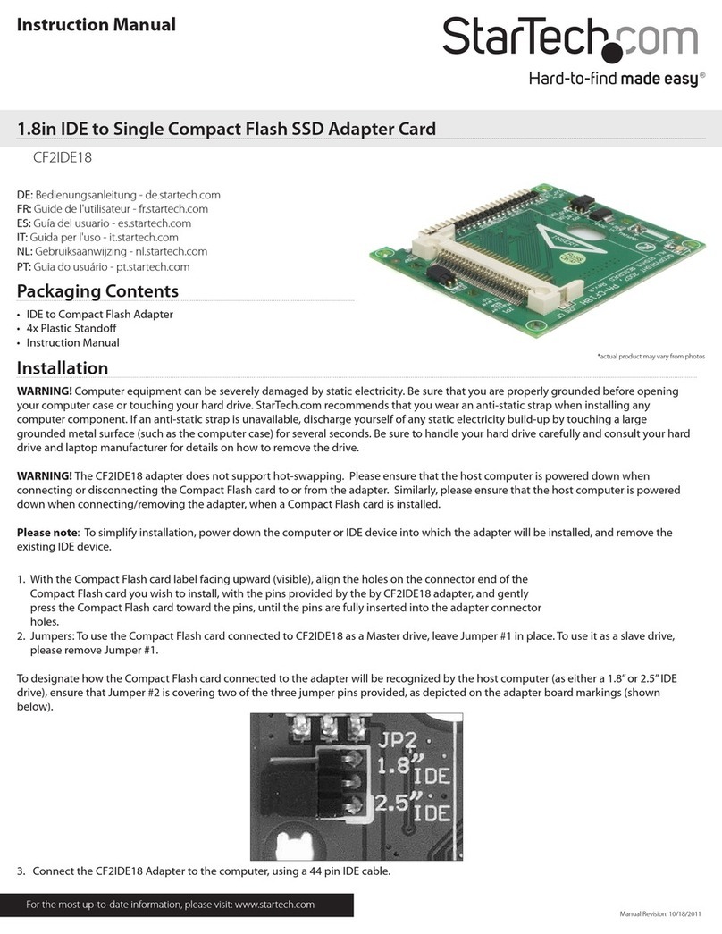
HOLT HI-15691 User manual

QSG-15691 Rev. New Holt Integrated Circuits
ADK-15691 Quick Start Guide –
HI-15691 Transceiver
Demonstration Board
February 7, 2022

QSG-15691
QSG-15691 Rev. New Holt Integrated Circuits
2
REVISION HISTORY
Revision Date Description of Change
QSG-15691 Rev. New 02/7/2022 Initial Release

QSG-15691
QSG-15691 Rev. New Holt Integrated Circuits
3
Introduction
The Holt HI-15691 is a MIL-STD-1553 5.0V CMOS transceiver which is drop-in alternative to the DDC BU-
63152G2. The ADK-15691 Demo Board provides a convenient way to evaluate the device features.
HI-15691PC Signal Break-Out Board
Set Up
To demonstrate the board, use the provided external power adapter providing 7.5 or 9.0 VDC at 1A.
Connect 3.3V or 5V to TP5 or J1 Pin21 or 23 to enable U2 5V regulator that powers the HI-15691. This
controlling voltage on TP5 can be used to sequence power on the HI-15691 by a host controller. JP11 is
shorted so the 5 volts from the voltage regulator is connected to the HI-15691.

QSG-15691
QSG-15691 Rev. New Holt Integrated Circuits
4
Host Electrical Interface
The HI-15691 is a 5V device but logic inputs as low as 2V from a host are acceptable. For optimum
performance consider 3.3V or 5V logic levels.
The HI-15691 logic RX and nRX outputs swing 0 to 4V (minimum). With light loads the outputs should
reach near 5V. If the host uses 2.5V or 3.3V input logic levels and cannot accommodate 5V signals from
the HI-15691, on-board padding resistors can be used to reduce the voltage. See the schematic for the
existing values which are set to reduce 5V to 3.3V already.
Power Supply
The board uses an external 7.5 or 9.0 VDC 1A power adapter. A MOSFET senses the presence of 3V3 on
J1 and turns on power to the 5V voltage regulator to power the HI-15691. This allows the 5V to be time
sequence when the 3V3 is present so everything powers up at the same time as a FPGA or host
controller. This feature could be bypassed if an external 5V is connected directly to TP6.
Bus Receive Signal Path
RXA and nRXA are the inverted and non- inverted receiver outputs for Bus A; RXB and nRXB are the
receiver outputs for Bus B. The logic-level Bus A and Bus B receiver outputs can be enabled/disabled
using the transceiver RXENA and RXENB inputs. The transceiver will output receive signals to the host
controller (if RX enable pins are high) when the bus has 1553 signaling per the data sheet and the
diagram shown below.

QSG-15691
QSG-15691 Rev. New Holt Integrated Circuits
5
Bus Transmit Signal Path
A pair of CMOS logic-level inputs accepts bipolar serial signals for driving each bus from an external user-
provided Manchester encoder. Transmit for each bus can be enabled or inhibited using the
corresponding TXINH transmit inhibit signal. The transmit signal path for each bus includes the bipolar
TX and nTX signals generated by the external Manchester encoder. Signal quality concerns dictate that
the TX/nTX signals for each bus have matched characteristics. This includes matched conductor length
and impedance, matched layer-to-layer vias (or even better, no vias). It is not always possible to achieve
good matching on the board layout. The result: TX and nTX switching transitions are not quite
simultaneous; the TX/nTX crossover occurs early or late. Crossover should occur mid-way between
ground and the 2.0 – 5V V to assure acceptable “output symmetry” or “tail-off” occurring at the end of
long transmit messages. This effect is discussed at length in Holt application note AN-550.
When the host applies TX and nTX signals the HI-15691 will transmit to the 1553 bus as shown below
providing the Transmit Inhibit pins are low. See AN-550 for tail-off considerations and if using a FPGA to
generate the TX and nTX signals, experience has demonstrated performance is optimized with higher
drive levels.

QSG-15691
QSG-15691 Rev. New Holt Integrated Circuits
6
Flexible 1553 Bus Interface Configuration
The HI-15691 Signal Break-Out Board has several options for configuring both MIL-STD-1553 bus
interfaces. The options are listed here and fully described below:
•Direct-Coupled or Transformer-Coupled bus interface for normal 1553 connectivity. Do not use
on-board termination resistors R5 and R6 (JP4 and JP9 must be open) in normal mode.
Open
Closed
Transformer
Ratio
Transformer
Coupled (Default)
JP1, JP5
JP6, JP10
JP2, JP3
JP7, JP8
1:1.79
Direct Coupled
JP2, JP3
JP7, JP8
JP1, JP5
JP6, JP10
1:2.5
•An On-board resistive dummy bus load suitable for Transformer Coupled or off-board
conventional bus connection. For Direct Coupled mode, change R5 and R6 to 35 ohms or use
external 35 ohm resistors. Transformer-coupled can use 70 or 78 ohm 1W resistors. For normal
1553 connectivity do not use the on-board termination resistors.
•Optional ground connections for negative side of Buses A and B so that single conventional
oscilloscope probes conveniently provide differential “Bus-Positive minus Bus-Negative” signal
viewing.
Direct-Coupled or Transformer-Coupled Operation
Direct-coupled 1553 bus interface is also known as a “short stub” connection because the terminal’s
stub cable cannot exceed 12 inches (31 mm) in length. Direct-coupled bus interface requires a pair of
current-limiting resistors in series with the bus connection. When configuration jumpers are set for
direct-coupled operation, current-limiting resistors are provided on the break-out board.
Transformer-coupled 1553 bus interface is the predominant configuration used for terminal connection.
This diagram shows a network comprised of three transformer-coupled terminals: a Bus Controller (BC)
and two Remote Terminals (RTs). Stub cables must be < 20 feet (6.1 meters).

QSG-15691
QSG-15691 Rev. New Holt Integrated Circuits
7
The HI-15691 Signal Break-Out Board (and user-provided protocol logic) takes the place of the BC or one
of the RTs in the above diagram.
As seen above, each terminal’s stub cable connects to the 1553 bus through a “bus coupler,” which is
typically an off-the-shelf hardware component comprised of coupling transformer(s) for one or more
terminal stubs (each with its own pair of internal current-limiting resistors). Two bus couplers are shown
above. The bus couplers have a bus connection jack at each end for serial connection into the 1553 bus
structure. Each end of the bus has a 78Ω terminator. Holt application note AN-550 provides additional
information about the direct- and transformer-coupled configurations.
Single Scope Probe “Faux Differential” Viewing Option
When characterizing a 1553 terminal, most bus measurements are the differential line-to-line stub
voltage measured across the bus side of the terminal’s isolation transformer. For the HI-15691 signal
break-out board, the transformer is the PM-DB27428 rectangular black cube, and the red and black
differential test point pairs are labeled BUSA/nBUSA and BUSB/nBUSB for the two buses.
Differential line-to-line voltage measurement for Bus A can be accomplished by connecting oscilloscope
probes for channel 1 and channel 2 to the BUSA and nBUSA test points respectively, and using scope
built-in math function to observe “channel 1 minus channel 2”. The user can forgo the channel 2
oscilloscope connection to nBUSA; the single channel 1 probe connection to BUSA provides true
differential viewing of Bus A stub voltage with nBUSA grounded. This is strictly a convenience measure

QSG-15691
QSG-15691 Rev. New Holt Integrated Circuits
8
to be used when evaluating HI-15691 transceiver performance; the minus side of the 1553 bus stub
would never be left grounded under normal circumstances for production hardware.
The above comments for configuring Bus A also apply for Bus B, substituting test points BUSB and
nBUSB for test points BUSA and nBUSA respectively.
Summary,
See AN-550 for tail-off, recommended power supply decoupling capacitors values and PCB layout
information.
Board Files and Schematic Links
BOM and Schematic Files: EV-15691
Table of contents
Other HOLT Computer Hardware manuals