Huawei GAQ40S3V3B User manual

1
GLOBAL ENERGY EFFICIENCY SPECIALIST
Copyright© 2012 Huawei Technologies Co., Ltd. All Rights Reserved.
THIS DOCUMENT IS FOR INFORMATION PURPOSE ONLY, AND DOES NOT CONSTITUTE ANY KIND OF WARRANTIES.
Description
The GAQ40S3V3B is a new generation isolated
DC-DC converter that uses an industry standard
quarter-brick structure, and features high
efficiency and power density, operates from an
input voltage range of 36 V to 75 V, provides the
rated output voltage of 3.3 V and the maximum
output current of 40 A.
Control Features
Remote on/off
Remote sense
Output voltage trim
Protection Features
Input undervoltage protection
Output overcurrent protection (hiccup mode)
Output short circuit protection (hiccup mode)
Output overvoltage protection (hiccup mode)
Overtemperature protection (self-recovery)
Safety Features
UL60950-1 and CSA C22.2 No. 60950-1-07
Meet UL94V-0 flammability requirements
RoHS6 compliant
Operational Features
Input voltage: 36 - 75 V
Output current: 0 - 40 A
Low output ripple and noise
Efficiency: 93.5% (3.3 V, 40 A) GAQ40S3V3B
Quarter-Brick
DC-DC Converter 36 - 75 V
Input 3.3 V Output 40 A Current Negative
Logic
GAQ40S3V3B
DC-DC Converter Technical Manual V1.4
Mechanical Features
Industry standard quarter-brick (D x W x H,
with a baseplate): 57.9 mm x 36.8 mm x 12.7
mm (2.28 in. x 1.45 in. x 0.50 in.)
Weight: about 58 g

2
GLOBAL ENERGY EFFICIENCY SPECIALIST
1. All dimensions in mm [in.]
Tolerances: x.x ±0.5 mm [x.xx±0.02 in.]
x.xx ±0.25 mm [x.xxx ±0.010 in.]
2. Pin 1-3, 5-7 are 1.00 ±0.05 mm [0.040 ±
0.002 in.] diameter with 2.00 ±0.10 mm
[0.080 ±0.004 in.] diameter standoff
shoulders.
Pin4 and pin8 are 1.50 ±0.05 mm [0.060
±0.002 in.] diameter with 2.50 ±0.10 mm
[0.098 ±0.004 in.] diameter standoff
shoulders.
3. M3 Screw used to bolt unit’s baseplate to
other surfaces (such as heatsink) must
not exceed 3.00 mm (0.120 in.) depth
below the surface of baseplate.
GAQ40S3V3B
DC-DC Converter Technical Manual V1.4
GAQ 40 S 3V3 B
1 2 3 4 5
Pin Description
1 —48Vin, high performance, analog control quarter-brick
2 —Output current: 40 A
3 —Single output
4 —Output voltage: 3.3 V
5 —With a baseplate
Designation Explanation
Mechanical Diagram
Pin No. Function
1 Vin (+)
2 On/Off
3 Vin (–)
4 Vout (–)
5 Sense (–)
6 Trim
7 Sense (+)
8 Vout (+)

3
GLOBAL ENERGY EFFICIENCY SPECIALIST
GAQ40S3V3B
DC-DC Converter Technical Manual V1.4
Parameter Min. Typ. Max. Units Notes & Conditions
Absolute maximum ratings
Input voltage
Continuous
Transient (100 ms)
-
-
-
-
80
100
V
V
-
-
Operating ambient
temperature -40 - 85 ºC See the thermal derating curve
Storage temperature -55 - 125 ºC -
Operating humidity 5 - 95 % RH Non-condensing
Input characteristics
Operating input voltage 36 48 75 V -
Maximum input current - - 4.5 A Vin = 36 V; Iout = 40 A
No-load loss - 3.6 - W Vin = 48 V; Iout = 0 A
Input capacitance 47 100 - µF Aluminum electrolytic capacitor
Inrush transient - - 1 A²s -
Input reflected ripple current
(peak to peak) - - 20 mA Oscilloscope bandwidth: 20 MHz
Output characteristics
Output voltage set point 3.25 3.3 3.35 V Vin = 36 - 75 V; Iout = 40 A
Output power 0 - 132 W -
Output line regulation - - ±0.20 % Vin = 36 - 75 V; Iout = 40 A
Output load regulation - - ±0.30 % Vin = 48 V; Iout = 0 - 40 A
Regulated voltage precision - - ±3 % Vin = 36 - 75 V; Iout = 0 - 40 A
Temperature coefficient - - 0.02 %Vout /°CTA= -40°C to +85°C (-40°F to +185°F )
External capacitance 470 - 104 µF -
Output current 0 - 40 A -
Output ripple and noise
(peak to peak) - 80 120 mV Oscilloscope bandwidth: 20 MHz
Output voltage Trim range 80 - 110 % -
Output voltage overshoot - - 5 % The whole range of Vin , Iout and TA
Output voltage rise time - 5 20 ms The whole range of Vin , Iout and TA
Switching frequency - 310 - kHz -
Electrical Specifications
Conditions: TA= 25°C (77°F), Airflow = 1 m/s (200 LFM), Vin = 48 V, unless otherwise notes.

4
GLOBAL ENERGY EFFICIENCY SPECIALIST
GAQ40S3V3B
DC-DC Converter Technical Manual V1.4
Parameter Min. Typ. Max. Units Notes & Conditions
Protection characteristics
Input undervoltage protection
Startup threshold
Shutdown threshold
Hysteresis
31
30
1
34
33
-
36
35
3
V
V
V
-
-
-
Output overcurrent protection 44 - 56 A Hiccup mode
Output short circuit protection - - - - Hiccup mode
Output overvoltage protection 3.9 - 4.7 V Hiccup mode
Overtemperature protection
Threshold
Hysteresis
115
5
125
-
135
-
°C
°C
Self-recovery
The values are obtained by measuring the
temperature of the hottest power
component on the top surface of the
convertor
Dynamic characteristics
Overshoot amplitude
Recovery time -
- -
- 100
100 mV
µs Current change rate: 0.1 A/µs
load : 25% - 50% - 25%; 50% - 75% - 50%
Overshoot amplitude
Recovery time -
- -
- 180
320 mV
µs Current change rate: 1 A/µs
load : 25% - 50% - 25%; 50% - 75% - 50%
Efficiency
100% load 91.0 93.5 - % Vin = 48 V; Iout = 40 A; TA=25°C (77°F)
50% load 88.0 93.5 - % Vin = 48 V; Iout = 20 A; TA= 25°C (77°F)
20% load 75.0 87.5 - % Vin = 48 V; Iout = 8 A; TA= 25°C (77°F)
Isolation characteristics
Input-to-output Isolation
voltage - - 1500 V DC Functional Isolation
Other characteristics
Remote on/off voltage
Low level
High level
-0.7
3.5
-
-
1.2
12
V
V
-
-
On/Off current
Low level
High level
-
-
-
-
1.0
-
mA
µA
-
-
Reliability characteristics
Mean time between failures
(MTBF) - 1.5 - Million
hours Telcordia SR332; 80% load; Airflow =
1.5m/s (300 LFM); TA= 40°C (104°F)
Electrical Specifications
Conditions: TA= 25°C (77°F), Airflow = 1 m/s (200 LFM), Vin = 48 V, unless otherwise notes.

5
GLOBAL ENERGY EFFICIENCY SPECIALIST
GAQ40S3V3B
DC-DC Converter Technical Manual V1.4
Figure 1: Efficiency (TA= 25°C or 77°F)
Figure 2: Power dissipation (TA= 25°C or 77°F)
Characteristic Curves
Figure 3: Thermal derating with airflow from Vin to
Vout (Vin = 48 V; Vout = 3.3 V) Figure 4: Thermal derating with airflow from Vin(–)
to Vin(+) (Vin = 48 V; Vout = 3.3 V)

6
GLOBAL ENERGY EFFICIENCY SPECIALIST
GAQ40S3V3B
DC-DC Converter Technical Manual V1.4
Typical Waveforms
Figure 8: Output voltage ripple
(for point B in the test set-up diagram, Vin = 48 V;
Vout = 3.3 V; Iout = 40 A)
Figure 7: Input reflected ripple current
(for point A in the test set-up diagram, Vin = 48 V;
Vout = 3.3 V; Iout = 40 A)
Is
Figure 5: Test set-up diagram
1. During the test of input reflected ripple current, the input terminal must be connected to a 12 µH inductor and a 220 µF
electrolytic capacitor.
2. Point B, which is for testing the output voltage ripple, is 25 mm (0.98 in.) away from the Vout(+) pin.
25 mm (0.98 in.)
12 µH
DC-DC
converter
A B
47 µF
Electrolytic
capacitor
10 µF
Tantalum
capacitor
470 µF
Tantalum
capacitor
0.1 µF
Ceramic
capacitor
Vin(+)
Vin(–)
Vout(+)
Vout(–)
Vsource
220 µF
Electrolytic
capacitor
Figure 6: Typical circuit applications
F1: 7 A fuse (fast blowing)
Cin: The high-frequency, low equivalent series resistance
(ESR) electrolytic capacitor (100 µF/100 V) is
recommended.
Co1: The 1 µF ceramic capacitor is recommended.
Co2: The 470 µF tantalum capacitor is recommended.
Vin(+)
On/Off
Vin(–)
Vout(+)
Sense(+)
Trim
Sense(–)
Vout(–)
Cin
S1
F1
Co1 Co2
EMI
filtering
Vout
Load Load
Vsource

7
GLOBAL ENERGY EFFICIENCY SPECIALIST
GAQ40S3V3B
DC-DC Converter Technical Manual V1.4
Figure 11: Startup by power on Figure 12: Shutdown by power off
Vout
Vout
Vin
Vin
Figure 9: Startup from On/Off Figure 10: Shutdown from On/Off
Conditions: TA= 25°C (77°F), Vin = 48 V.
Vout
On/Off
Vout
On/Off
Typical Waveforms
Iout
Vout Vout
Iout
Figure 13: Output voltage dynamic response
(Load: 25% - 50% - 25%, di/dt=0.1 A/µs) Figure 14: Output voltage dynamic response
(Load: 50% - 75% - 50%, di/dt=0.1 A/µs)

8
GLOBAL ENERGY EFFICIENCY SPECIALIST
Remote On/Off
Figure 15: various circuits for driving the On/Off pin
Logic
Enable On/Off Pin Level Status
Negative
logic Low level On
High level or left
open Off
Remote Sense
Output Voltage Trim
Trim Up
The relationship between Radj-up and Vout:
Vin(+)
On/Off
Vin(–)
Vout(+)
Sense(+)
Trim
Sense(–)
Vout(–)
Radj-up Load
)(2.10
510
225.1 )100(1.5 kohm
V
Rnom
upadj
100
nom
nom
uptrim
VVV
Figure 17: Configuration diagram for Trim up
The output voltage can be increased by installing
an external resistor between the Trim pin and the
Sense(+) pin.
1. If the Trim pin is not used, it should be left open.
2. Ensure that the actual output power does not exceed
the maximum output power when raising the voltage.
The output voltage can be adjusted according to
the trim range specification by using the Trim pin.
Trim Down
The output voltage can be decreased by installing
an external resistor between the Trim pin and the
Sense(–) pin.
Figure 18: Configuration diagram for Trim down
The relationship between Radj-down and Vout:
Vin(+)
On/Off
Vin(–)
Vout(+)
Sense(+)
Trim
Sense(–)
Vout(–)
Radj-down
Load
)(2.10
510 kohmR downadj
100
nom
downtrimnom
V
VV
Simple control
On/Off
Vin(–)
On/Off
Vin(–)
On/Off
Vin(–)
On/Off
Vin(–)
Transistor control
Isolation control Direct logic drive
VCC
TTL/
COMS
GAQ40S3V3B
DC-DC Converter Technical Manual V1.4
Figure 16: Configuration diagram for remote sense
This function is used to compensate for voltage
drops on Rw. The Sense(+), Sense(–), Vout(+), and
Vout(–) terminals should meet the following
requirements:
Vin(+)
On/Off
Vin(–)
Vout(+)
Sense(+)
Trim
Sense(–)
Vout(–)
Rw
Load
Rw
Rwindicates the line impedance between the output terminal
and the load.
If the remote sense function is disabled, the
Sense(+) terminal directly connects to the Vout(+)
terminal and the Sense(–) terminal directly
connects to the Vout(–) terminal.
[Vout(+) –Vout(–)] –[Sense(+) –Sense(–)] ≤ 10% x Vnom
(Vnom is the rated output voltage.)

9
GLOBAL ENERGY EFFICIENCY SPECIALIST
GAQ40S3V3B
DC-DC Converter Technical Manual V1.4
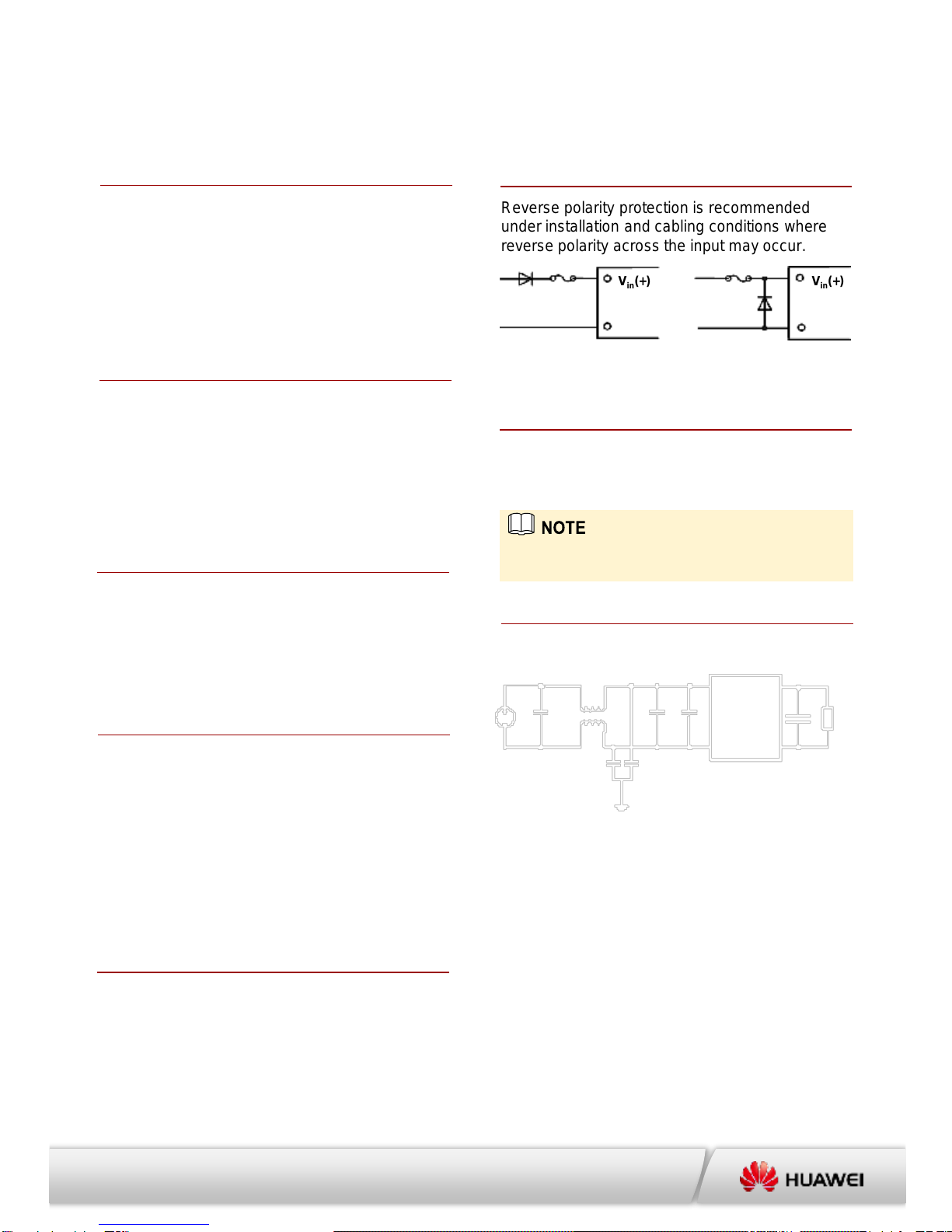
Reverse polarity protection is recommended
under installation and cabling conditions where
reverse polarity across the input may occur.
Vin(+)
Vin(–)
Vin(+)
Vin(–)
The converter has no internal fuse. To meet
safety and regulatory requirements, a 7 A fuse is
recommended.
For the acceptance standard, see the DC-DC
Converter EMC Acceptance Manual.
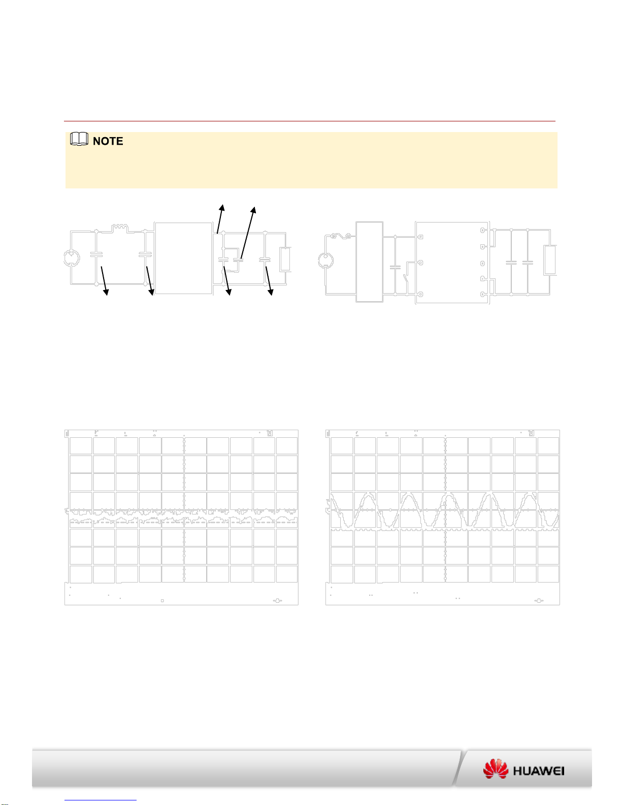
Recommend Reverse Polarity
Protection Circuit
Figure 19: Recommend reverse polarity protection
circuits
Recommended Fuse
EMC
Figure 20: EMC test set-up diagram
DC-DC
converter Load
C1 L1
C4 C5
C2 C3 C6
Vin(+)
Vin(–)
Vout(+)
Vout(–)
C1: Surface mount device (SMD) ceramic capacitor (100
V/1000 nF/X7R/1210)
C2: SMD ceramic capacitor (100 V/100 nF/±10%/X7R/1206)
L1: Common-mode inductor (single phase, 1320 µH/±25%/4
A/R5K/ 21 mm x 21 mm x 12.5 mm [0.83 in. x 0.83 in. x 0.49
in.]). The chip component with the same specifications can also
be used.
C4, C5: High-pressure resistant chip ceramic capacitor (22
nF/1000 V/X7R/1210)
C3: Electrolytic capacitor (100 µF/100 V)
C6: Electrolytic capacitor (470 µF/25 V)
Vs
The fuse current should be 1.5 to 2 times the maximum
operating current in actual use.
Input Undervoltage Protection
The converter will shut down after the input
voltage drops below the undervoltage protection
threshold for shutdown. The converter will start
to work again after the input voltage reaches the
input undervoltage protection threshold for
startup. For the Hysteresis, see the Protection
characteristics.
Output Overcurrent Protection
The converter equipped with current limiting
circuitry can provide protection from an output
overload or short circuit condition. If the output
current exceeds the output overcurrent
protection set point, the converter enters hiccup
mode. When the fault condition is removed, the
converter will automatically restart.
Output Overvoltage Protection
When the voltage directly across the output pins
exceeds the output overvoltage protection
threshold, the converter will enter hiccup mode.
When the fault condition is removed, the
converter will automatically restart.
Overtemperature Protection
A temperature sensor on the converter senses
the average temperature of the module. It
protects the converter from being damaged at
high temperatures. When the temperature
exceeds the overtemperature protection
threshold, the output will shut down. It will allow
the converter to turn on again when the
temperature of the sensed location falls by the
value of Overtemperature Protection Hysteresis.
MTBF
The MTBF is calculated according to the
Telcordia, SR332 Method 1 Case3.

10
GLOBAL ENERGY EFFICIENCY SPECIALIST
GAQ40S3V3B
DC-DC Converter Technical Manual V1.4
Parameter Units Condition
High Accelerated Life
Test (HALT) 4 Lowest operating temperature: -60°C (-76°F); highest operating
temperature: 110°C (230°F); vibration limit: 40 G
Proof Of Screen (POS) 4 80 temperature cycles; 50% vibration limit stress: 20 G
High Accelerated
Stress Audit (HASA) 8 4 temperature cycles; 50% vibration limit stress: 20 G
Thermal Shock 32 500 temperature cycles between -40°C (-40°F) and +125°C (+257°F)
with the temperature change rate of 20°C (68°F) per minute
Lasting for 30 minutes both at -40°C (-40°F) and +125°C (+257°F)
Temperature Humidity
Bias 16 85°C (185°F); 85% RH; 1000 operating hours under lowest load
power
Qualification Testing
Sufficient airflow should be provided to ensure reliable operating of the converter. Therefore, thermal
componentsare mounted on the top surface of the converter to dissipate heat to the surrounding
environment by conduction, convection and radiation. Proper airflow can be verified by measuring the
temperature at the middle of the baseplate.
The temperature at the thermal test point on the converter cannot exceed
105°C (221°F). Otherwise, the converter will be protected against
overtemperature and will not operate properly.
Thermal Consideration
Figure 21: Thermal test point
Thermal Test Point
Power Dissipation
The converter power dissipation is calculated based on efficiency. The following formula reflects the
relationship between the consumed power (Pd), efficiency (ŋ), and output power (Po): Pd=Po(1-η)/η
Middle of the base plate

11
GLOBAL ENERGY EFFICIENCY SPECIALIST
GAQ40S3V3B
DC-DC Converter Technical Manual V1.4
Mechanical Consideration
Installation
Although the converter can be mounted in any direction, free airflow must be taken.
Soldering
HUAWEI TECHNOLOGIES CO., LTD.
Huawei Industrial Base Bantian Longgang
Shenzhen 518129
People's Republic of China
www.huawei.com
The converter is compatible with standard wave soldering techniques. When wave soldering, the
converter pins should be preheated for 20 - 30 seconds at 110°C (230°F) , and wave soldered at 260°C
(500°F) for less than 10 seconds.
When hand soldering, the iron temperature should be maintained at 425°C (797°F) and applied to the
converter pins for less than 5 seconds.
The converter can be rinsed using the isopropyl alcohol (IPA) solvent or other proper solvents.
Table of contents
Other Huawei Media Converter manuals

Huawei
Huawei NAD12S10-A User manual

Huawei
Huawei IRD6000 User manual

Huawei
Huawei GAQ37S12B-4 User manual

Huawei
Huawei R4815N1 User manual

Huawei
Huawei SUN2000 Series User manual

Huawei
Huawei ADF10S48B User manual

Huawei
Huawei GDQ54S12B-4A User manual

Huawei
Huawei DEC6108 User manual

Huawei
Huawei MERC Smart PV Optimizer User manual