HYCON HY17S68 Series Instructions for use

HY17S68 Series
HY17S68-DK03 IDE
Hardware User’s Manual
© 2020 HYCON Technology Corp
www.hycontek.com
APD-HY17PIDE007-V01_EN
page2
Table of Contents
1. PACKAGE CONTENTS ............................................................................................................................4
2. SAFETY PRECAUTIONS .........................................................................................................................5
3. SOFTWARE INSTALLATION REQUIREMENTS.....................................................................................6
3.1. IDE Software Installation Requirements ...............................................................................................6
4. DESCRIPTION OF THE HARDWARE TOOL ..........................................................................................7
4.1. Schematic architecture description .......................................................................................................7
4.2. Description of control box .....................................................................................................................7
4.3. Description of In-Circuit Emulator(ICE) Board ......................................................................................9
4.4. ICE board circuit diagram ................................................................................................................... 11
4.5. Control box and ICE board hardware connection steps .....................................................................12
5. REVISION RECORD...............................................................................................................................13

HY17S68 Series
HY17S68-DK03 IDE
Hardware User’s Manual
© 2020 HYCON Technology Corp
www.hycontek.com
APD-HY17PIDE007-V01_EN
page3
Attention:
1、HYCON Technology Corp. reserves the right to change the content of this datasheet
without further notice. For most up-to-date information, please constantly visit our
website: http://www.hycontek.com .
2、HYCON Technology Corp. is not responsible for problems caused by figures or
application circuits narrated herein whose related industrial properties belong to third
parties.
3、Specifications of any HYCON Technology Corp. products detailed or contained herein
stipulate the performance, characteristics, and functions of the specified products in the
independent state. We does not guarantee of the performance, characteristics, and
functions of the specified products as placed in the customer’s products or equipment.
Constant and sufficient verification and evaluation is highly advised.
4、Please note the operating conditions of input voltage, output voltage and load current
and ensure the IC internal power consumption does not exceed that of package
tolerance. HYCON Technology Corp. assumes no responsibility for equipment failures
that resulted from using products at values that exceed, even momentarily, rated values
listed in products specifications of HYCON products specified herein.
5、Notwithstanding this product has built-in ESD protection circuit, please do not exert
excessive static electricity to protection circuit.
6、Products specified or contained herein cannot be employed in applications which
require extremely high levels of reliability, such as device or equipment affecting the
human body, health/medical equipments, security systems, or any apparatus installed in
aircrafts and other vehicles.
7、Despite the fact that HYCON Technology Corp. endeavors to enhance product quality
as well as reliability in every possible way, failure or malfunction of semiconductor
products may happen. Hence, users are strongly recommended to comply with safety
design including redundancy and fire-precaution equipments to prevent any accidents
and fires that may follow.
8、Use of the information described herein for other purposes and/or reproduction or
copying without the permission of HYCON Technology Corp. is strictly prohibited.

HY17S68 Series
HY17S68-DK03 IDE
Hardware User’s Manual
© 2020 HYCON Technology Corp
www.hycontek.com
APD-HY17PIDE007-V01_EN
page4
1. Package Contents
HY17S68-DK03 is an integrated hardware development kit, including ICE
(In-Circuit Emulator) Board, Control Box, LCD Board and USB Cable. Integrated hardware
development kit helps to develop MCU application program of HY17P6x Series. Through
the NB/PC end connection for program compilation and debugging functions, the relevant
hardware equipment is as follows:
Model No.
Part Name
Description
Quantity
HY17S68-DK03
1. HY17S68-IM03
HY17S68-L216 ICE Board
1
2. HY17000-CM01
HY17S Control Box
1
3. HY10000-AM02
LCD Board(For DMM)
1
4. Cable line
USB Type A to Mini. B Cable
1
5. Interface line
6pin/2.54 (2.54mm pitch)
1
Table 1-1
Note: HY17S68-DK03 development tool is mainly dedicated to the development of
HY17P68 multimeter (DMM) products.

HY17S68 Series
HY17S68-DK03 IDE
Hardware User’s Manual
© 2020 HYCON Technology Corp
www.hycontek.com
APD-HY17PIDE007-V01_EN
page5
2. Safety Precautions
Do not place heavy objects on the display panel, in order to avoid damage caused by
stress.
Place the application display boards at steady place, so as to avoid falling damage.
Do not use this product with the input voltage which is not meeting the electrical
specifications, in order to avoid working abnormally or damage.
Avoid application display boards being touched by liquid, dirt and avoid being exposed
to moisture during operation. This application should be kept in a dry environment, so
as not to affect the function and performance.
Remove the power supply when not using it.
When following status occurred, please remove the power supply immediately, and
contact our engineer.
Power Supply line is worn or damaged.
Power source (battery) connected but no any light on while operating.
Component off.

HY17S68 Series
HY17S68-DK03 IDE
Hardware User’s Manual
© 2020 HYCON Technology Corp
www.hycontek.com
APD-HY17PIDE007-V01_EN
page6
3. Software Installation Requirements
3.1. IDE Software Installation Requirements
Minimum System Requirements of operating HY17S68 IDE hardware development tool:
(1) PC/NB hardware requirement
IBM PC compatible X86 system CPU
512 MB Memory (1GB recommended)
1GB Hard disk
(2) Supported product model
HY17P68
(3) Hardware support models
HY17S68-DK03: HY17S68 IDE hardware development tool
(HY17000-CM01 supports firmware version above W15P02.0)
(4) Software supported version
HY17P IDE V1.2 version above:HY17P Series Assembly Language IDE software
H08 CIDE V1.2 version above:HYCON 8-bit MCU C Language IDE software
(5) Operating system requirements
Windows XP, Windows Vista, Windows 7, Windows 8, Windows 10
(6) Applicable interface mode
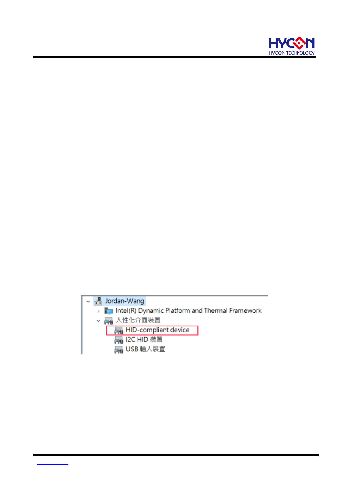
USB Port with HID-compliant device
HY17S68-DK02's USB Port driver uses the Windows standard HID driver
(Figure 3-1), so user can use it without installing a separate driver.
Figure 3-1

HY17S68 Series
HY17S68-DK03 IDE
Hardware User’s Manual
© 2020 HYCON Technology Corp
www.hycontek.com
APD-HY17PIDE007-V01_EN
page7
4. Description of the hardware tool
4.1. Schematic architecture description
HY17000-CM01 (control box) is the connecting device between HY17S68-IM03 ICE
Board and HY17P Series IDE software.
Connect with HY17S68-IM03 ICE board through Interface line (6Pin/2.54mm).
Connect with HY17P Series IDE software through USB line, the connection diagram is
as follows:
Figure 4-1
4.2. Description of control box
The control box (model: HY17000-CM01) is universal for HY17P series products (as shown
in Figure 4-2). The following is the introduction of the control box:
HY17P
HY17000-CM01
POWER LED
USB Port
IDE Port
Figure 4-2
(1) Power LED
Function:POWER LED
Item
Name
Description
L1
Power LED
Green light, when the USB Port is connected to a computer
or a 5V power supply through a USB cable, when the
green light is on, it means that the control box is normally
powered.

HY17S68 Series
HY17S68-DK03 IDE
Hardware User’s Manual
© 2020 HYCON Technology Corp
www.hycontek.com
APD-HY17PIDE007-V01_EN
page8
(2) IDE Port
Function: IDE communication interface, used to connect with the Debug interface of
the ICE Board to control the chip.
The function is defined as follows:
Item
Name
Description
1
VSS
Power ground
2
SCK
SCK Pin of Control Box and ICE board
3
VDD
Power output 4.5V
4
CS
CS Pin of Control Box and ICE board
5
SDI
SDI Pin of Control Box and ICE board
6
SDO
SDO Pin of Control Box and ICE board
(3) USB Port
Function:USB Port
Description: Mini B Cable connector

HY17S68 Series
HY17S68-DK03 IDE
Hardware User’s Manual
© 2020 HYCON Technology Corp
www.hycontek.com
APD-HY17PIDE007-V01_EN
page9
4.3. Description of In-Circuit Emulator(ICE) Board
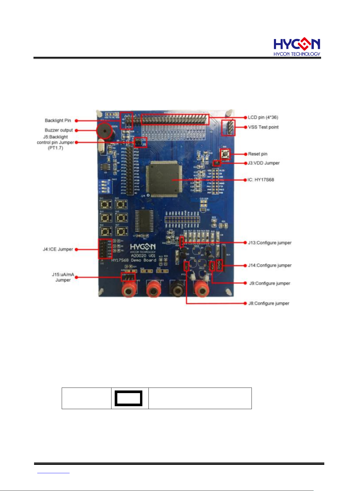
The ICE board (model: HY17S68-IM03) is commonly used for HY17P68 (see Figure 4-3).
This ICE board is mainly used for IDE hardware tools, which can be used to simulate chips
and develop debugging. The following describes the appearance and functions of the ICE
board:
Figure 4-3
(1) Backlight pin
Function: LCD backlight end (A.K pin)
(2) Buzzer output
Function: can make the buzzer sound
(3) J5: Backlight control pin Jumper
Function: When Jumper is short-circuited, select the preset backlight control pin as
PT1.7
J5
∙
∙
When shorted, the backlight
control pin is PT1.7
(4) J4: ICE Jumper
Function: connect with the control box (HY17000-CM01) to simulate the operation of the
chip.

HY17S68 Series
HY17S68-DK03 IDE
Hardware User’s Manual
© 2020 HYCON Technology Corp
www.hycontek.com
APD-HY17PIDE007-V01_EN
page10
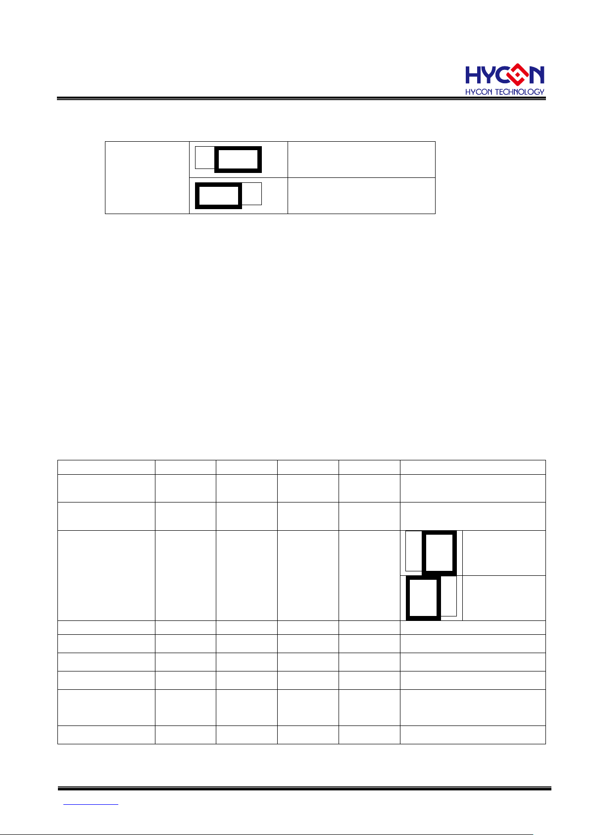
(5) J15: uA/mA Jumper
Function: measuring current usage
J15
∘
∙
∙
Right shorted, current
range mA measurement
∙
∙
∘
Left shorted, current
range uA measurement
(6) LCD pin (4COM*36SEG)
Function: Mainly control the use of LCD display
(7) VSS Test point
Function: Use for grounding test
(8) Reset pin
Function: Reset ICE to use.
(9) J3:VDD Jumper
Function: Provide HY17S68 power supply (4.5V)
(10) IC: HY17S68
Function: Simulation chip, used to simulate the use of HY17P68
(11) ~ (14) Configure jumper
Function: According to different measurement functions, the configuration settings of
Jumper are as follows:
Function
J13
J14
J9
J8
J15
DC mV
AC mV
Open
Open
Short
Open
Open
DCV
ACV
Short
Open
Open
Open
Open
DC Current
AC Current
Open
Open
Open
Open
∘
∙
∙
mA
measurement
∙
∙
∘
uA
measurement
Resistor
Open
Open
Short
Short
Open
Continuity
Open
Open
Short
Short
Open
Diode
Open
Open
Short
Short
Open
Capacitor
Open
Open
Short
Short
Open
Frequency
(CNT Input)
Open
Short
Short
Short
Open
Thermocouple
Open
Open
Short
Open
Open

HY17S68 Series
HY17S68-DK03 IDE
Hardware User’s Manual
© 2020 HYCON Technology Corp
www.hycontek.com
APD-HY17PIDE007-V01_EN
page11
4.4. ICE board circuit diagram
1
1
2
2
3
3
4
4
5
5
6
6
D D
C C
B B
A A
Title
Number RevisionSize
C
Date: 2020/7/22 Sheet of
File: D:\PCB\A20020_V01\A20020 V01.schdocDrawn By:
HY17S68 ICE Board
V01A2020
_VCC_ram
_VSS_ram
_SDI
_SDO
_SCK
_SCS
R4
47K
R5
47K
R9
47K
VDD_bat
12 34 56 78 910 1112
J4
ICE
_SDI
_SDO
_SCK
_SCS
_VCC_ram
_VSS_ram
_ADR14
_ADR11
_ADR13
_ADR10
_ADR9
_ADR8
_DA7
_DA6
_DA5
_DA4
_DA3
_RD
_WE
VDD_bat
Program/SBM Memory
A5
5A6
4A7
3
A8 25
A9 24
A10 21
A11 23
A12
2
A13 26
A14
1
I/O0
11
I/O1
12
I/O2
13
I/O3 15
I/O4 16
I/O5 17
I/O6 18
I/O7 19
CE 20
A0
10
OE 22
A1
9A2
8A3
7A4
6
WE 27
GND
14
VCC 28
U2
62256
_VSS_ram
_ADR12
_ADR7
_ADR6
_ADR5
_ADR4
_ADR3
_ADR2
_ADR1
_ADR0
_DA2
_DA1
_DA0
_VSS_ram
*. ICE Memory NET
VDD_bat
_CS
C7
0.1uF
VSS
28
PB0
29
PB1
30
PB2
31
PB3
32
PB5
34
PB6
35
PB7
36
OP1O
39
OP1N
40
RLU
41
RLD
45
PA0
46
PA1
47
PA2
48
PA3
49
PA4
50
PA5
51
PA6
52
PA7
57
PA8
58
FTP
74
FTN
75
AGND
76
REFO
77
VDDA
78
RST/VPP
79
VGG
80
CA
81
CB
82
VDD
83
VLCD
84
COM0/PSCK
85
COM1/PSDI
86
COM2/PSDO
87
COM3
88
SEG2/PT6.4
89
SEG3/PT6.5
90
SEG4/PT6.6
103
SEG5/PT6.7
104
SEG6/PT7.0
105
SEG7/PT7.1
106
SEG8/PT7.2 111
SEG9/PT7.3 112
SEG10/PT7.4 113
SEG11/PT7.5 114
SEG12/PT7.6 115
SEG13/PT7.7 116
SEG14/PT8.0 117
PB4
33
ICE_ADR13
25
ICE_ADR14
26
ICE_ADR10
22
ICE_ADR11
23
ICE_ADR12
24
ICE_ADR9
21
ICE_ADR6
18
ICE_ADR7
19
ICE_ADR8
20
ICE_DA5
4
ICE_DA6
5
ICE_DA7
6
ICE_ADR0
9
ICE_ADR1
10
ICE_ADR2
14
ICE_ADR3
15
ICE_ADR4
16
ICE_ADR5
17
ICE_CS
7
ICE_CS0
8
ICE_DA4
3
NC2
11
NC3
12
NC4
13
NC8
44
NC6
42
NC7
43
VSS_ICE
27
NC10
54 NC9
53
NC12
56 NC11
55
NC14
62 NC13
61
NC16
64 NC15
63
NC18
66 NC17
65
NC20
68 NC19
67
NC22
70 NC21
69
NC24
72 NC23
71
NC37
107
NC38
108
PB8
37
PB9
38
PA9
59
PA10
60
PA11
73
NC39 109
NC40 110
SEG15/PT8.1 122
SEG16/PT8.2 123
SEG17/PT8.3 124
SEG18/PT8.4 125
SEG19/PT8.5 126
SEG20/PT8.6 127
SEG21/PT8.7 128
SEG22/PT9.0 129
SEG23/PT9.1 130
SEG24/PT9.2 131
SEG25/PT9.3 132
SEG26/PT9.4 133
SEG27/PT9.5 134
SEG28/PT9.6 135
SEG29/PT9.7 136
SEG30/PT10.0 137
SEG31/PT10.1 138
SEG32/PT10.2 139
SEG38/PT11.0 145
SEG39/PT11.1 146
SEG40/PT11.2 147
SEG41/PT11.3 148
PT1.0/INT1.0/SDI 149
NC45 150
NC46 151
NC47 152
PT1.2/INT1.2/LVDIN 154
PT1.3/INT1.3/RC 155
PT1.4/INT1.4/TX 156
PT1.5/INT1.5/SDO/TBI1 157
PT1.6/INT1.6/SCK 158
PT1.7/INT1.7 159
NC51 160
PT1.1/INT1.1/SCE/TBI0 153
PT2.1/XTI/INT2.1 165
PT2.2/INT2.2/SCL 166
PT2.3/INT2.3/SDA 167
PT2.4/INT2.4/BZ 168
PT2.5/INT2.5 179
PT2.6/INT2.6 180
PT2.7/INT2.7/TBI2 181
PT3.0 182
PT3.1 183
PT3.2 184
PT3.3 185
PT3.5/PWM1 187
PT3.6/CNT 188
PT3.7/CMP 189
PT4.0 190
PT4.1 191
PT4.2 192
PT3.4/PWM0 186
PT4.3 193
PT4.4 194
ICE_VCC 195
ICE_SDI 198
ICE_SDO 197
ICE_SCK 199
ICE_RD 200
ICE_WE 196
ICE_DA0 211
ICE_DA1 212
ICE_DA2 213
ICE_DA3 214
SEG33/PT10.3 140
SEG34/PT10.4 141
SEG35/PT10.5 142
SEG36/PT10.6 143
SEG37/PT10.7 144
NC0
1
NC1
2
NC72 215
NC73 216
NC25
91
NC26
92
NC27
93
NC28
94
NC29
95
NC30
96
NC31
97
NC32
98
NC33
99
NC34
100
NC35
101
NC36
102
NC41 118
NC42 119
NC43 120
NC44 121
NC48 161
NC49 162
NC50 163
PT2.0/XTO/INT2.0 164
NC52 169
NC53 170
NC54 171
NC55 172
NC56 173
NC57 174
NC58 175
NC59 176
NC60 177
NC61 178
NC62 201
NC63 202
NC64 203
NC65 204
NC66 205
NC67 206
NC68 207
NC69 208
NC70 209
NC71 210
U4
HY17S68_LQFP216
_ADR14
_ADR12
_ADR7
_ADR6
_ADR5
_ADR4
_ADR3
_ADR2
_ADR9
_ADR8
_ADR10
_ADR11
_ADR13
_DA7
_DA6
_DA5
_DA4
_WE
_RD
_DA3
_DA2
_DA1
_DA0
_ADR1
_ADR0
_SCK
_SDI
_SDO
VSS
SW2
Select
SW3
Hz/Duty
SW4
Relative
SW6
Manual Hold/Backlight
SW5
Range
SW7
Maximum Hold/Peak Hold
KEY1
KEY2
KEY5
KEY4
KEY3
VSS
1
2
3
4
8
7
6
5
SW10
Function
VDD_bat
VSS
1
2
3
4
J12
Uart
NC
1
NC
2
NC
3
SDA 5
SCL 6
WP 7
VSS
4
VCC 8
U3
NC/24C02
VSS
C6
NC/1uF R8
NC/4.7K
R7
NC/4.7K
VDD_batVDD_bat
VDD_bat
RC
TX SDA
SCL
SEG11
SEG12
SEG13
SEG14
SEG15
SEG16
SEG17
SEG18
SEG19
SEG20
SEG21
SEG22
SEG23
SEG24
SEG25
SEG26
SEG27
SEG28
SEG29
SEG30
SEG31
SEG32
SEG8
SEG9
SEG10
FUN1
FUN2
FUN3
FUN4
SEG34
SEG36
SEG35
SEG37
SEG33
COM0
COM1
COM2
COM3
SEG2
SEG3
SEG4
SEG5
SEG6
SEG7
SDA
SCL
PSDO
PSDI
PSCK
PB0
PB1
PB2
PB3
PB4
PB5
PB6
PB7
PB8
PB9
PA0
PA1
PA2
PA3
PA4
PA5
PA6
PA7
PA8
PA9
PA10
RC
TX
C11
0.1uF
R27
NC/100k
C18
0.47uF
VSS
SW1
RST
VDD
RST
VLCD
VGG
RST
REFO
FTN
FTP
VDDA
AGND
VDD
VPP
C12
1uF
C13
1uF C14
1uF
VSSA
VSS
VSSVSS
C17
1uF
C15
1uF
C20
0.1uF
AGND ACOM
VSSA
C10
27nF
PA11
PT10
PT11
PT12
PT13
PT14
PT15
PT16
PT17
PT20
PT21
PT22
PT23
PT24
PT25
PT26
PT27
PT30
PT31
PT32
PT33
BUZZER1
BUZZER
VSS
VSS
Y1
4.9152MHz
R6
1M
C4
15pF
C5
15pF
XOUT
XIN
LVDIN
KEY1
KEY2
KEY3
KEY4
FUN2
FUN3
FUN4
PT34
PT35
PT36
PT37
PT40
PT41
PT42
CNT
CMP
KEY5
PT43
PT44
R13
100K
該COM點代表直接拉回AGND
ACOM
OP1O
OP1N
VDD_bat
_CS
_SCS
R10
0R
VSSA
VSS
P4
COM
P2
mA/uA
P3
A
R33
10K
PB3
R24
10K
PB1
R25
99R
R29
0.99
R32
0.01
1
2
3
J15
Current
uA
mA
ACOM
該COM點代表直接拉回AGND
OP1N
R30
10K/1%
R26
90.9K/1%
OP1O
Internal OPA1
ACOM
R31
1M
AGND
C16
1uF
PB5
ACV/ACmV Coupled for
Frequency Measurement
R20 1.11M 0.1%
R18 101K 0.1%
R17 10K 0.1%
R16 1K 0.1%
R19 10M
ACOM
J13
Volt
C8 0.1uF
RLU
RLU
RLD
VDDA
R28
NC/10K
C19
NC/10uF
PB4
1 2
3
D2
NC/LM385
VSS
J14
HZ
CNT
C9
1uF R23
1M
R22
100R
R21
1M
VDD
VSS
RLD
P1
Vol/Ohm/Cap/DT
R12
900K
R15
100R
ACOM
R14
10M 0.7%
J9
Vol/Ohm/Cap/DT
B2
C
1E3
Q3
8050
B2
C1
E
3
Q4
8050
PA6
ACOM
B2
C1
E
3
Q2
8050
B2
C
1E3
Q1
8050
J8
Vol/Ohm/Cap/DT
MOV3
TVR
MOV1
TVRMOV2
TVR ACOM
PTC1
PTC
PTC2
PTC
CA
CB
_VSS_ram R11
0R
_VSS_ram
VSSA
PT24
VSS
Backlight
FUN1
SCK
SDI
SDO
CS
R35
220
R36
100K
R34
4.7K
VSS VSS
VDD
B
B
CC
E
E
Q5
8050/SOT23
1 2
3 4
5 6
7 8
9 10
11 12
13 14
15 16
17 18
19 20
21 22
23 24
25 26
27 28
29 30
31 32
33 34
35 36
37 38
39 40
41 42
43 44
45 46
47 48
49 50
J2
Header 25X2
A
KA
K
COM0
COM2
SEG2
SEG4
SEG6
SEG8
SEG10
SEG12
SEG14
SEG16
SEG18
SEG20
SEG22
SEG24
SEG26
SEG28
SEG30
SEG32
SEG34
SEG36
COM1
COM3
SEG3
SEG5
SEG7
SEG9
SEG11
SEG13
SEG15
SEG17
SEG19
SEG21
SEG23
SEG25
SEG27
SEG29
SEG31
SEG33
SEG35
SEG37
A
K
VDD_bat
VDD
1
2
J3
Current test
_VCC_ram
* Current Test Port
1
2
3
4
JP1
VSS
VSS
1
2
J5 Blacklight_JMPER
Figure 4-4
Note:The ICE board circuit diagram is placed in the IDE software folder,
"A20020 V01_HY17S68-IM03_HY17S68-L216 ICE Board.pdf"
The Assembly IDE folder path is: "HYCON\HY17P IDE\ICESchematic"
The H08 CIDE folder path is: "HYCON\H08 CIDE\ICESchematic\HY17P"

HY17S68 Series
HY17S68-DK03 IDE
Hardware User’s Manual
© 2020 HYCON Technology Corp
www.hycontek.com
APD-HY17PIDE007-V01_EN
page12
4.5. Control box and ICE board hardware connection steps
(1) Confirm that J3 (VDD Jumper) of the ICE board is short-circuited together.
(2) The Interface lines are respectively connected to the IDE port of the control box
and the ICE Jumper (J4) of the ICE board.
(3) Use USB Cable to connect to the USB Port of the control box and the USB Port of
the computer (the Power LED will be on at this time).
(4) After Step1~3 (as shown in Figure 4-5), it means that the hardware of the control
box and the ICE board are properly connected.
Figure 4-5
Other manuals for HY17S68 Series
1
This manual suits for next models
1
Table of contents
Other HYCON Computer Hardware manuals
Popular Computer Hardware manuals by other brands

Z Systems
Z Systems z-K6 manual

Cypress Semiconductor
Cypress Semiconductor CY7C1361C Specification sheet

Arbor Technology
Arbor Technology EmETXe-i89U0 Quick installation guide

Mobility Sound
Mobility Sound BTD-2N4-5 user manual

Cicada Audio
Cicada Audio DSP88 owner's manual

AustSTEM
AustSTEM Kookaberry Quick manual