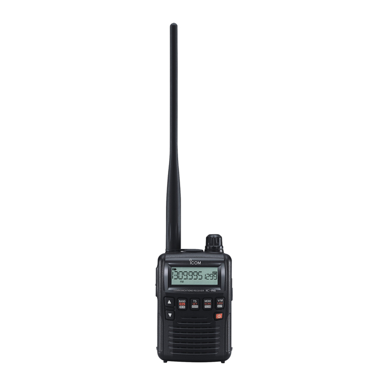
Icom IC-R10 User manual

o
ICOM
SERVICE
MANUAL

INTRODUCTION
This service manual describes the latest information for the IC-R10 at the tinrre of
publication.
MODEL VERSION SYMBOL
U.S.A. USA
IC-H10 France FRA
U,K, UK
Europe EUR
DANGER
NEVER connect the receiver to an AC outfet or to aDC power supply that uses
more than 16 V. Such aconnection could cause afire hazard and/or electric
shock.
DO NOT expose the receiver to rain, snow or any liquids.
DO NOT reverse the polarities of the power supply when connecting the
receiver.
DO NOT apply an RF signai ol more than 20 dBm (100 mW) to the antenna
connector. This could damage the receiver's front end,
ORDERING PARTS
Be sure to include the following four points when ordering replacement parts:
1. 10-digit order numbers
2. Component pari number and name
3. Equipment model name and unit name
A. Quantity required
^SAMPLE ORDER>
1110001310 S.IC TA7363F IC-RIO MAIN UNIT Ipiece
3310009560 Screw FHM2x6ZK(BT} IC-RlO CHASSIS 7pieces
Addresses are provided or> the inside back cover for your convenience.
REPAIR NOTES
1.Make sure aproblem is internal before disassembling the receiver.
2. DO NOT open the receiver until the receiver is discormected from its power
source.
3. DO NOT force any of the variable components. Turn them slowly and
smoothly.
4. DO NOT short any circuits or electronic parts. An insulated tuning tool MUST
be used for all adjustments.
5. DO NOT keep power ON for along time when the receiver is defective.
6. READ the instructions of test equipment thoroughly before connecting
equipment to the receiver.
I

TABLE OF CONTENTS
SECTION 1SPECIFICATIONS
SECTION 2INSIDE VIEWS
SECTION 3DISASSEMBLY INSTRUCTIONS
SECTION 4CIRCUIT DESCRIPTION
4-1RECEIVER CIRCUITS 4-1
4-2 PLL CIRCUITS 4-4
4-3POWER SUPPLY CIRCUITS 4-5
4-4CPU PORT ALLOCATIONS 4-6
SECTION 5ADJUSTMENT PROCEDURES
5-1 PLL AND BFO ADJUSTMENT 5-1
5-2COMMAND ADJUSTMENT (ADJUSTMENT SET MODE) 5-3
SECTION 6PARTS LIST
SECTION 7MECHANICAL PARTS AND DISASSEMBLY
SECTION 8SEMI-CONDUCTOR INFORMATION
SECTION 9BOARD LAYOUTS
SECTION 10 BLOCK DIAGRAM
SECTION 11 VOLTAGE DIAGRAM

SECTION 1SPECIFICATIONS
GENERAL
•Frequency range
•Mode
•Tuning steps
•Power supply requirement
•Current drain (at 13.5 VDC)
•Usable temperature range
•Antenna connector
•Scan speed
•Cl-V connector
•Dimensions (projections not included)
•Weight
RECEIVER
•Receive system
•Intermediate freq.
•Sensitivity
(typical, except spurious points)
•Squelch sensitivity (at threshold)
•Selectivity
•Audio output power (at 13.5 VDC)
•External speaker connector
VERSION FREQUENCY RANGE
Europe, U.K. 500 kHz-1 300 MHz
France 500 kHz-87.5 MHz
108 MHz-1300 MHz
U.S.A.
500 kHz-823.9999 MHz
849.0001-
868.9999 MHz
894.0001-
1300 MHz
:FM, WFM, AM, USB, LSB, CW
:0.1, 0.5, 1,5, 6.25, 8, 9, 10, 12.5, 15, 20, 25, 30, 50, 100 kHz or
user-programmable (0.1-999.9 kHz/0.1 kHz steps)
4.8 VDC (4 AA (R6) Ni-Cd cells); or, 4.8-1 6VDC acceptable (negative ground)
Rated audio 180 mA typ.
Standby 110 mA typ.
Power saved 38 mA typ.
-10°C to +50°C; +14“F to +122T
BNC (50 Q)
16.7 ch/sec. (programmed scan), 6.25 ch/sec. (memory scan)
3-conductor 3.5 (d) mm (Vs")
58.5 (W) X130 (H) X31 .3 (D) mm; 2.3 (W) x5.1 (H) x1-2 (D) in
310 g; 10.9 oz.
Triple-conversion superheterodyne
1St 266.7 MHz (340.0000-999.9999 MHz)
429.1 MHz (except above freq.)
2nd 10.7 MHz
3rd 455 kHz
FREQUENCY (MHz) FM AM SSB/CW
0.5 -4.9999 —1.6 pV 0.40 pV
5.0 -74.9999 0.32 pV —1.0 pV 0.25 pV
75.0- 199.9999 1.0 pV
200.0 -339.9999 0.45 pV 2.2 pV 1.6 pV 0.40 pV
340.0 -699.9999 0.35 pV 1.3 pV 1.4 pV 0.32 pV
700.0 -799.9999 0.79 pV 2.0 pV 2.0 pV 0.63 pV
800.0 -899.9999 1.6 pV 0.40 pV
900.0 -1300.0000 —
*FM and WFM are measured at 12 dB SINAD; AM, SSB and CW are measured at 10 dB S/N.
FREQUENCY (MHz) FM WFM AM
0.5 -4.9999 0.50 pV —1.6 pV
5.0 -74.9999 0.32 pV —1.0 pV
75.0- 199.9999 1.0 pV
200.0 -339.9999 0.45 pV 2.2 pV
340.0- 699.9999 0.35 pV 1.3 pV EDH
700.0 -799.9999 2.0 pV
800.0 -899.9999 1.6 pV
900.0 -1300.0000 —
SSB, CW More than 4kHz /6 dB
AM, FM More than 15 kHz/6 dB
WFM More than 150 kHz/6 dB
More than 120 mW at 10% distortion with an 8Qload
3-conductor 3.5 (d) mm (V8")/8 Q
1-
1

3rd IF arnplilier
qirculi
2nci IF amplifier
(Q2i'2SCJ2i&
tMam band]
IF 1C (Sub-bandi -
(,tC47l ;TA31 136F)
Top view
SSB detector circuit
BFO ampliJier (Q95t:2SC42ltj
2nd IF amplifier (Q42l :2SC42V5
Sub-band)
3rd IF circuit (SSB/CW)
3fd tF circuit (AM /FM)
2id IF circuit (WFM]
AF amplifier (IC361 :TA73eaF)
IF 1C
(IC?1 :TA3i 136F /Mam band)
AF sv/ilch (IC301 :BU4066CFV)
2nd miJter
(Q41 1 : 2SC50&5 /Sub-band)
DATA expander 1C
(IC3D5: BU4094BF)
2nd mixer 1C
(I Cl 1: ^lPC27ST /Main band)
2nd PLL 1C (I C50 1:MP03 14063)
VXO circuit
2nd refatenca oscillaior
Bottom view (x&d icr-sss n2,e mhz)
RF amplifier
(Q5l:2SC42i5> —
1sl miser IC —
^
(IC271; MPC276T)
RF circuit —=
(700 MHz -1.30D MHz)
RF circuit
(300 MHz '500 MHZ)“
RF circuit ——
—
(30 MHz -75 MHi)
RF circuit —
-
[O.&MHZ' 1.9 MHz}
RF circuit
{15 MHz -3D MHZ)
iStlFcircuH ——
”
{340 MHz '1GHz)
Tw/^
r
Reference cscillaior.
{X501; 10,345 MHz)
Top view
4-
RF circuit
<500 MHZ -700 MHz)
RF circuit
<75 MRz -300 MHz)
RF circuit
<1.9 MHZ -15 MHz)
tsMF amphlier (Q421;2SC4226)
1st IF circuit
(0.5 MHz -340 MHz and
1GHz -1.3 GHz}
1st VCO unit
Bottom view
•LOGIC unit
Bottom view
AF mute switch
flC950: TC43D6F)
CPU IC
(IC1: pP07B054GK]
VSC fC
(IC201: MPC5D23-115)
AF amplifier
(0950: 3SC4211)
BFO Circuit
2-1

SECTION 3DISASSEMBLY INSTRUCTIONS
•Opening the case
®Remove the SP cap, O-
@Unscrew 6screws, Oand 0to open the case.
•Removing the LOGiC unit
®Unplug J1 to separate the front panel and rear panel.
@Unsolder 2points Oand unscrew 4 screws 0.
(D Remove the LOGIC unit in the direction of the arrow.
iJ^Be careful when pulling, pull up, LCD components are
on the opposite side.
•Removing the MAiN unit
®Unscrew 3screws ©.
(D Remove the MAIN unit in the direction of the arrow.
•Removing the RF unit
®Remove 3knobs Oand unscrew 3nuts 0.
@Unsolder 4points 0and unscrew 3screws ®.
@Remove the RF unit in the direction of the arrow.
Note
•)KWhen pulling the terminals, the ©side of each
terminals has apiece of rubber affixed.
3-1

4-1 RECEIVER CIRCUITS
4-1-1 ANTENNA SWITCHING CIRCUIT (RF UNIT)
Received signals enter the RF unit from the antenna
connector (J1) and pass through alimiter (D1) and an
attenuator circuit (D2). The signals are then applied to the
RF circuit via the antenna switching circuit (D51, D151,
D171, D211, D231) which suppress out-of-band signals.
4-1-2 RF CIRCUIT (RF UNIT)
The RF circuit amplifies the received signals within the
range of frequency coverage and filters out-of-band signals.
(1)
0.5 MHz-74.9999 MHz signals
RF signals (0.5 MHz-74.9999 MHz) from an antenna
switching circuit (D51) pass through alow-pass filter (L51,
L52). The filtered signals are amplified at an RF amplifier
(Q51) through each bandpass filter depending on the
receiving frequency. The amplified signals are then applied
to the 1st mixer circuit (IC271) through the band switching
diode (D253).
The signals below 1.9 MHz pass through alow-pass filter
(L55, L56) via the band switching diode (D52), and are then
applied to the RF amplifier circuit (Q51) via the band
switching diode (D53).
The 1.9 MHz-29.9999 MHz signals pass through the band
switching diode (D61) and low-pass filter (L61, L62). The 1.9
MHz-14.9999 MHz signals pass through the band switching
diode (D81) and bandpass filter (L82, L83, L91, L92), and
are then applied to the RF amplifier circuit (Q51) via the
band switching diode (D82).
The 15.0 MHz-29.9999 MHz signals pass through the band
switching diode (D101) and high-pass filter (LI 02, LI 03)
and are then applied to the RF amplifier circuit (Q51) via the
band switching diode (D102).
•RF filters
Receive frequency
[MHz] sw
diodes BPF select
signal Components
0.5- 1.8999 D52, 053 80 L55, L56
1.9-14.9999 D81 ,082 81 L82, L83, L91, L92
15.0-29.9999 0101, 0102 82 L102, LI 03
30.0 -74.9999 0121, 0122 83 L122, L123
The 30,0 MHz-74.9999 MHz signals pass through the band
switching diode (D121) and high-pass filter (LI 22, LI 23),
and are then applied to the RF amplifier circuit (Q51) via the
band switching diode (D122).
(2) 75.0 MHz-199.9999 MHz
The 75.0 MHz-199.9999 MHz signals pass through the
tunable bandpass filter (D152, LI 52) via the band switching
diode (D151), and are then amplified at the RF amplifier
(Q151) and pass through another tunable bandpass filter
(D153, LI 55). The filtered signals are applied to the 1st
mixer circuit (IC271) via the band switching diode (D154).
(3) 200.0 MHz-499.9999 MHz
The 200.0 MHz-499.9999 MHz signals pass through the
tunable bandpass filter (D172, LI 72) via the band switching
diode (D171), and are then amplified at the RF amplifier
(Q171) and pass through another tunable bandpass filter
(D173, LI 75). The filtered signals are applied to the 1st
mixer circuit (IC271)via the band switching diode (D1 74).
(4) 500.0 MHz-699.9999 MHz
The 500.0 MHz-699.9999 MHz signals pass through a
tunable band pass filter (D213, L213, L214) via the band
switching diode (D211), and are then amplified at an RF
amplifier (Q211) and pass through another tunable
bandpass filter (D214, L216, L217). The filtered signals are
applied to the 1st mixer circuit (IC271) via the band
switching diode (D154).
(5) 700.0 MHz-1300.0000 MHz
The 700.0 MHz-1300 MHz signals pass through ahigh-
pass filter (L232, L233) via the band switching diode (D231),
and are then amplified at the RF amplifier (Q231) and pass
through atunable bandpass filter (D238, L240). The filtered
signals are applied to the 1st mixer circuit (IC271) via the
band switching diode (D236).
•Tunable band pass filters and RF amplifiers
Receive frequency
[MHz] .
BPF select
signal
Varactor
diodes RF amplifier
84 0152, 0153 Q151
200.0- 499.9999 85 0172, 0173 Q171
500.0- 699.9999 86 0213, 0214 Q211
700.0- 1300.0000 87 0238 Q231
RF filter and amplifier circuits
D152, D153, D172, D173, D213, D214 and D238 employ
varactor diodes that are controlled by the CPU (LOGIC unit;
IC1 )to track the bandpass filter. These varactor diodes tune
the center frequency of an RF passband for wide width
receiving and good image response rejection.
4-1-3 1ST MIXER AND 1ST IF CIRCUITS {RF UNIT)
The 1st mixer circuit converts the received RF signals to a
fixed frequency of the 1st IF signal with the PLL output
frequency. By changing the PLL frequency, only the desired
frequency will pass through the band pass filters at the next
stage of the 1st mixer.
The amplified signals are mixed with 1st LO signals from the
1st VCO unit at a1st mixer (IC271) to produce 1st IF signals
(266.7 MHz; 340.0 MHz-999.9999 MHz, 429.1 MHz; 0.5
MHz-339.9999 MHz and 1.0 GHz-1 .3 GHz).
The 1st IF signals are applied to each IF filter (FI401 for
266.7 MHz IF signal, FI411 for 429.1 MHz IF signal) to
suppress out-of-band signals. The 1st IF signals are
amplified at the 1st IF amplifier (Q421) and then applied to
the 2nd mixer on the MAIN unit.
•1st LO frequency and 1st IF frequency
Receive frequency
[MHz]
1st LO frequency
[MHz]
1st IF frequency
[MHz]
0.5- 339.9999 429.6 -769.0999 429.1
340.0- 609.9999 606.7 -876.6999 266.7
610.0- 999.9999 343.3 -733.2999 266.7
1000.0- 1300.0000 733.3 -870.9000 429.1
4-1-4 2ND MIXER AND 2ND IF CIRCUIT
(MAIN UNIT)
The 2nd mixer circuit converts the 1st IF signal to a2nd IF
signal.
The 1st IF signals (266.7 MHz or 429.1 MHz) from the RF
unit are applied to the 2nd mixer circuit (IC11) for mixing
with the 2nd LO signals to be converted into a10.7 MHz
2nd IF signal. The 2nd IF signal is applied to the IF filter
(Fill) to suppress out-of-band signals, and is then amplified
at the 2nd IF amplifier (Q21 ).
4-1-5 3RD IF AND DEMODULATOR CIRCUIT
(MAIN UNIT)
The 3rd mixer circuit converts the 2nd IF signal to a3rd IF
signal.
IC71 contains the 3rd mixer, limiter amplifier, quadrature
detector, s-meter detector and noise detector circuits.
The 2nd IF signal (10.7 MHz) from the 2nd IF amplifier
(Q21) is applied to the 3rd mixer section of IF 1C (IC71, pin
16) and is then mixed with a10.245 MHz 3rd LO signal
generated by X501 on the RF unit for conversion to a455
kHz 3rd IF signal. The 3rd IF signal is demodulated at each
demodulator circuit.
(1)
FM
The 3rd IF signal from the 3rd mixer (1071, pin 3) passes
through the ceramic filter (FI111) to suppress unwanted
heterodyned frequency signals. It is fed back to 1071, then
amplified at the limiter amplifier section (pin 5) and applied
to the quadrature detector section (pin 10) to demodulate
the 3rd IF signal into AF signals. The AF signals are output
from pin 9and passed through the de-emphasis circuit
(R79, 086) with frequency characteristics of -6 dB/octave,
and then applied to the AF switch (10301 c, pin 4).
Aportion of the AF signals from pin 9(1071) passes through
the low-pass filter (R78, 084) and is applied to the OPU
(LOGIO unit; 101) as AFO control signals.
(2) WFM
The signal from the 3rd mixer is applied to the limiter
amplifier section (1071, pin 5). The amplified signals are
demodulated at the quadrature detector section (1071, pin
5). The AF signals are output from pin 9(1071) and are
applied to the AF switch (10301c, pin 4) the same as in FM
mode.
By connecting R81 to R72 in parallel, the output
characterstics of pin 12, “RSSI”, change gradually.
Therefore, the FM IF 10 can detect WFM components.
(3) AM
The signal from the 3rd mixer passes through the ceramic
filter (FI111) and is amplified at the 3rd IF amplifiers (Q151,
Q161). The amplified signal is demodulated at the AM
detector (Q171). The demodulated AF signals are applied to
the AF switch (10301 d, pin 8) via the ANL control circuit
(Q172).
•2nd IF, 3rd IF and demodulator circuit
IC71
to AF switch
IC301
4-2

(4) SSB/CW
The signal from the 3rd mixer passes through the ceramic
filter (FI101) and is amplified at the 3rd IF amplifiers (Q151,
Q161) and buffer amplifier (Q201). The amplified signals
are applied to the SSB/CW detector (D201 ,D202) and
mixed with BFO signals from the BFO circuit (LOGIC unit;
X231) via the BFO amplifier (0951) to demodulate AF
signals. The demodulated AF signals are applied to the AF
switch (IC301b, pin 11) after being pre-amplified at the AF
pre-amplifier (0202).
•Bandpass filter selection
Mode(s) Bandpass filter(s) Passband width
NFM /AM FI111 15 kHz
SSB /CW FI101 4kHz
WFM ——
4-1-6 SUB-BAND RECEIVER CIRCUIT (MAIN UNIT)
The sub-band receiver circuit is employed by the band
scope and SIGNAVI functions.
Aportion of the 1st IF signals from the RF unit is mixed with
the sub 2nd LO signals at the 2nd mixer circuit (0411) to be
converted into 455 kHz sub 2nd IF signal. The 2nd IF signal
Is applied to the IF 1C (IC471 ,pin 5) via the IF filter (FI411)
and 2nd IF amplifier (0421). The IF 1C (IC471) outputs
signals to lead the CPU (LOGIC unit; IC1) under conditions
of RSSI or noise squelch.
4-1-8 SQUELCH CIRCUIT (MAIN UNIT)
Anoise squelch circuit cuts out AF signals when no RF
signal is received. By detecting noise components in the AF
signals, the CPU switches the AF mute switch.
Some of the noise components in the AF signals from IC71
(pin 9) are passed through the active filter (IC71 ,pins 8, 7),
and then applied to the noise detector section. The squelch
control pot (RF unit; R11) adjusts the input level of the
active filter, and the level is used for the squelch threshold
reference. The detected noise signals are applied to the
CPU (LOGIC unit; IC1, pin 65) via the “SQL” line. The CPU
then analyzes the noise condition and controls the “MUTE”
port to cut off the AF signal using the AF mute switch
(LOGIC unit; IC950).
4-1-9 VSC CIRCUIT (LOGIC UNIT)
The VSC (Voice Scan Control) detects AF signals and
mutes undesired signals such as unmodulated, beat and
noise component signals. When the VSC function is ON
and an unmodulated signal is received, squelch functions
the same as closed (no signal condition) even when it’s
open, or the scan function resumes for ashort period on
any scan setting during scanning.
Aportion of the AF signals from the low-pass filter (Q950) is
applied to the VSC control circuit (IC201) to detect
demodulated signals while the VSC function is ON. When
audio component signals are included in the AF signals, the
VSC 1C (IC201 )outputs alow level signal from pin 13 to the
CPU (IC1 ,pin 1)to release the mute switch (IC950).
4-1-7 AF AMPLIFIER CIRCUIT (MAIN UNIT)
The AF amplifier circuit amplifies the demodulated AF
signals to drive aspeaker.
The AF signals from the AF switch (IC301) are applied to
the LOGIC unit through a“DETOM” line. The AF signals are
amplified at the AF amplifier (LOGIC unit; 0950), and are
then applied to the AF mute switch (LOGIC unit; IC950).
The output signals from the AF mute switch (LOGIC unit;
IC950) are applied to the [VOL] control (RF unit; R11), and
are then power-amplified at the AF amplifier (MAIN unit;
IC361 ,pin 4) to drive aspeaker.
4-1-10 BFO CIRCUIT (LOGIC UNIT)
The BFO (Beat Frequency Oscillator) circuit consists of
X231, IC231 and D231. The oscillator provides abeat
frequency signal (USB; 456.5 kHz, LSB; 453.5 kHz) to the
SSB/CW detector circuit (MAIN unit; D201, D202) for
demodulating the 3rd IF signal into AF signals.
The oscillating frequency for each mode (LSB/USB/CW) is
switched by changing the capacitance of avaractor diode
(D231). When USB mode is selected, the CPU (IC1, pin 3)
outputs “LOW” level voltage to D231 to change the BFO
frequency to 456.5 kHz.
•Squelch and AF amplifier circuits
4-3

4-1-11 AGC CIRCUIT (MAIN UNIT)
The AGC (Auto Gain Control) circuit reduces IF/RF amplifier
gain to keep the audio output at aconstant level. The
receiver gain is determined by the voltage on the IF-AGC
line (Q182 collector) and RF-AGC line (RF unit; Q901
collector).
The 3rd IF signals from the 3rd IF amplifier (Q161) are
detected at the AM detector (Q171). Aportion of the
detected signals is applied to the AGC amplifiers (Q182 and
RF unit; Q901) as the AGC control voltage. The AM
detector (Q171) is used for the AGC detector in the AGC
circuit.
When receiving strong signals, the detected voltage
increases and the AGC voltage decreases via the AGC
amplifiers (Q182 and RF unit; Q901). As the AGC voltage is
used for the bias voltage of the IF/RF amplifiers, IF/RF
amplifier gain is decreased.
4-1-12 NOISE BLANKER CIRCUIT (MAIN UNIT)
The noise blanker circuit detects pulse-type noise, and
stops IF amplifier operation during detection.
Aportion of the 2nd IF signals from the 2nd IF amplifier for
the sub-band (Q421) is amplified at the noise amplifier
circuit (Q801, Q802). The amplified signal is recified at the
noise detector circuit (Q805) for conversion into DC voltage.
The DC voltage is applied to the NB control circuit (Q806,
Q807) to control the NB switch (Q810).
Some DC voltage is fed back to the noise amplifier circuit
(Q801 ,Q802) via the DC amplifier (Q808). The DC amplifier
functions as an AGC circuit to reduce averaged noise.
Therefore, the noise blanker function shuts off pulse-type
noise only.
4-2 PLL CIRCUITS
4-2-1 GENERAL
1ST/2ND LO PLL circuits (RF/MAIN units) provide stable
oscillation of the receive LO frequencies. The PLL circuit
consists of the PLL 1C (IC501 on the RF/MAIN units),
charge pump, loop filter and reference oscillator and
employs apulse swallow counter.
4-2-2 1ST LO PLL CIRCUIT (RF UNIT)
Signals from the 1ST VCO unit pass through the buffer
amplifier (Q551) and are prescaled in the PLL 1C (IC501,
pin 10) based on the divided ratio (N-data). The PLL 1C
detects the out-of-step phase using the reference frequency
and outputs it from pin 6. The output signal is passed
through the charge pump (Q521 ,Q522) and is applied to
the loop filter (R527, C527) to be converted into DC voltage
as aPLL lock voltage. The PLL lock voltage is applied to
the 1ST VCO unit via the VI Lline.
Aportion of the signal from the loop filter (R527, C527) is
amplified at the buffer amplifier (Q502) and is then applied
to the CPU (LOGIC unit; IC1) as the lock voltage
information (LVI). The CPU (pin 6) outputs a“TUNE” signal
based on the lock voltage; the voltage is amplified at the
buffer amplifiers (LOGIC unit; Q181, 0182) and is then
applied to the RF unit as the tunable bandpass filter control
signal (VTUNE). This signal (VTUNE) is used for the RF
tunable bandpass filters to match the filter’s center
frequency to the desired receive frequency.
4-2-3 REFERENCE OSCILLATOR CIRCUIT
(RF UNIT)
The reference oscillator circuit (X501, IC501) generates a
10.245 MHz reference frequency which is stabilized within
the temperature range -10°C (+14T) to +50°C (+122°F).
The reference frequency is applied to the PLL 1C and also
applied to the MAIN unit as the 3rd LO signal via the buffer
amplifier (0531).
4-2-4 1ST VCO CIRCUIT (1ST VCO UNIT)
The 1ST VCO circuit contains three separate VCO circuits
depending on the receive frequency. The oscillated signal at
one of the three VCO circuits is applied to the buffer
amplifier (0601). The amplified signal is applied to the RF
unit via the VI Oline and is then applied to the 1st mixer
circuit (RF unit; IC271, pin 3)as the 1st LO signal after
being amplified at the buffer amplifier (RF unit; 0552).
Aportion of the signal from the VI Oterminal (1ST VCO
unit; J601) is amplified at the buffer amplifier (0551) and is
then fed back to the PLL 1C (IC501, pin 10) as the
comparison signal.
•1st LO PLL circuit (RF unit)
4-4

.1st VCO
Receive frequency
[MHz]
VCO
select
signal
VCO
components VCO frequency
[MHz]
0.5- 199.9999 VII Q621, Q622,
D621 429.6 -629.0999
200.0- 533.2999 V12 Q641, D641 629.1 -799.9999
533.3 -609.9999 V13 Q661, D661,
D662 800.0 -876.6999
610.0- 895.7999 VII Q621.Q622,
D621 343.3 -629.0999
895.8- 999.9999 V12 Q641, D641 629.1 -733.2999
1000.0-1058.1999 VII 0621,0622,
D621 570.9 -629.0999
1058.2-1229.0999 V12 0641, D641 629.1 -799.9999
1229.1 -1300.0000 V13 0661, D661,
D662 800.0- 870.9000
4-2-5 2ND LO PLL CIRCUIT (MAIN UNIT)
The 2ND LO PLL circuit generates the 2nd LO frequency for
the main band (receive signal) and sub-band (band scope
and SIGNAVI functions).
Signals from the 2ND VCO unit pass through the buffer
amplifier (0531 for main band, 0551 for the sub-band) and
are applied to the PLL 1C (IC501; pin 2and pin 19
respectively) and prescaled in the PLL 1C based on the
divided ratio (N-data). The PLL 1C detects the out-of-step
phase using the reference frequency and outputs it from
pins 8and 13. The output signal from pin 8is passed
through the loop filter (R51 1,R51 2, R51 4, C51 1,C51 2), and
is then applied to the 2ND VCO circuit for the main band
(2ND VCO unit) via the 21 LV terminal (2ND VCO unit; J601)
as the lock voltage. The output signal from pin 13 is passed
through the loop filter (R521-R523, C521, C522), and is
then applied to the 2ND VCO circuit for the sub-band (2ND
VCO unit) via the 22LV terminal (2ND VCO unit; J601 )as
the lock voltage.
band (0411) after being amplified at the buffer amplifier
(0552). The switching transistors (0601 and 0701) shift the
oscillating frequencies via the “IFH" signal from the RF unit.
4-3 POWER SUPPLY CIRCUITS
VOLTAGE LINE (LOGIC UNIT)
Line Description
HV The voltage coming from the external DC jack.
VCC The same voltage as the installed battery cells or
HV line passed through the charge control circuit
(Q101.D104).
+3CPU
Common 3Vfor the CPU (ICl) produced at the
+3CPU regulator 1C (IC81). The circuit outputs
the voltage regardless of the power ON/OFF
condition.
+3S Common 3Vconverted from the VCC line by the
+3S regulator circuit (Q121, Q122) using a
control signal (+3SC) from the CPU.
+3C Common 3Vconverted from the VCC line by the
+3C regulator circuit (Q111, Q112) using a
control signal (3LCON) from the CPU.
+3L Common 3Vconverted from the VCC line by the
+3L regulator circuit (Q91 ,Q92) using acontrol
signal (3LCON) from the CPU.
+15 Common 15 Vconverted from the +3L line by
the DC-DC convertor iC (ICl 51).
4-2-6 VXO CIRCUIT (MAIN UNIT)
The VXO (Variable Crystal Oscillator) circuit (IC501, X501
and D501) generates a12.8 MHz 2nd reference frequency.
The 2nd reference frequency is stabilized within the
temperature range -10°C (+14°F) to +50°C (+122°F). For
tuning the 100 Hz frequency step, the VXO circuit changes
the capacitance of avaractor diode (D501 )via the voltage
of the “VXO” line from the CPU (LOGIC unit; IC1), and
controls the 2nd reference frequency.
4-2-7 2ND VCO CIRCUIT (2ND VCO UNIT)
The 2ND VCO unit contains two VCO circuits for the main
band and sub-band. The VCO circuit for the main band
consists of 0602, 0604 and D601 ,and the VCO circuit for
the sub-band consists of Q702, 0704 and D701. The
oscillated signal is amplified at the buffer amplifiers (0603
for the main band, 0703 for the sub-band). Then the 2nd
LO signal for the main band is applied to the 2nd mixer
(ICl 1,pin 3) via the buffer amplifier (0532), and the 2nd LO
signal for the sub-band is input to the 2nd mixer for the sub-
4-5

4-4 CPU PORT ALLOCATIONS
4-4-1 CPU (IC1 on the LOGIC unit) CPU (IC1) —continued
Pin
number Port
name Description
46 +3SC
Outputs control signal for the +3S
regulator circuit.
Low; During PLL unlock or power
save.
48 VSCC Outputs VSC control signals.
Low :When the VSC function is ON.
49 MUTE Outputs AF mute switch (IC950)
control signals.
Low ;While muted.
50 BEEP Output port for beep audio signals.
51 AFONC
Outputs acontrol signal for AF
amplifier regulator circuit.
High: When squelch is open.
(FM mode only)
52-59 1/00-1/07 Ouput ports for the LCD control data.
60 RESET Input port for the reset signal.
61 FUNG Input port for the [FUNC] switch.
Low :While [FUNC] switch is pushed.
62 POWSW Input port for the [PWR] switch.
Low: While [PWR] switch is pushed.
63 D-UD Input port for the [DIAL].
64 D-CK
65 SQL Input port for the main band noise
signals.
66 S-SQL Input port for the sub-band noise
signals.
73 UL Input port for PLL unlock signal from
the PLL ICs.
76 RSSI Input port for the main band receive
signal strength level.
77 CENT Input port for the AFC control voltage.
78 BInput port for the sub-band receive
signal strength level.
79 BATT Input port for connected voltage low
battery detection.
80 nInput port for the PLL lock voltage
information.
Pin
number Port
name Description
1VSC
Input port for VSC detected signals.
High: Unmodulated or beat signals
are received.
Low :Modulated signals are received.
3BFOS2 Output port for BFO control signal.
Low ;LSB/CW mode (453.5 kHz)
High: USB mode (456.5 kHz)
5VXO Output port for VXO frequency
control voltage.
6TUNE Outputs tunable band pass filter
control voltage.
8CLIN Input port for the cloning or Cl-V
control signals.
9CLOUT Output port for the cloning or Cl-V
control signals.
10 BF03
Output port for BFO regulator control
signal.
Low :While SSB/CW mode is
selected.
12 SDATA Outputs serial data signals to the PLL
ICs, EEPROM (LOGIC unit, 1C41)
and I/O expander ICs, etc.
13 SCK Outputs serial clock signal to the PLL
ICs, EEPROM (LOGIC unit, IC41)
and I/O expander ICs, etc.
14 ISTB Outputs strobe signals for the I/O
expander ICs.
15 VSCS
Outputs VSC-time constant control
signal.
High: While unmodulated signal or no
RF signal is received
Low :While receiving modulated
signals.
16 ESO Output port for serial data signals to
the EEPROM 1C (LOGIC unit, IC41).
17 ESI Input port for serial data signals from
the EEPROM 1C (LOGIC unit. IC41).
18 ESCK Output port for clock signal to the
EEPROM 1C (LOGIC unit, IC41).
19-22 KS0-KS3 Output strobe signals to the key
matrix.
25,26 PSTB1
,
PSTB2 Output strobe signals to the PLL ICs.
27-31 K0-K4 Input ports for the key matrix.
32, 34 MO, Ml Input ports for the initial matrix.
44 3LCON Outputs control signal for the +3C
and +3L regulator circuits.
High: While turning power ON.
45 LAMPO Outputs LCD and key backlight
control signal.
Low :While backlight is ON.

4-4-2 OUTPUT EXPANDER 1C
(1) MAIN UNIT, IC305 (3} RF UNIT, IC2
Pin
number Description
Outputs WFM mode select signals.
Low :When WFM is selected.
Outputs NFM mode select signals.
Low :When NFM is selected.
Outputs AM mode select signals.
Low :When AM is selected.
Outputs SSB mode select signals.
Low :When SSB is selected.
Outputs NB control signals.
Low ;When NB function is ON.
(SSB/CW mode only)
Outputs ANL control signals.
Low ;When ANL function is ON.
(AM mode only)
Outputs sub-band regulator control
S-PWC signals.
Low :While the bandscope or
SIGNAVI functionis activated.
Pin
number Port
name Description
BOC Outputs low-pass filter select signal
.
Low :When frequencies below 1.9
MHz are displayed.
B1C Outputs bandpass filter select signal.
Low ;When frequencies from 1.9 to
14.9999 MHz are displayed.
B2C Outputs bandpass filter select signal.
Low ;When frequencies from 15.0 to
29.9999 MHz are displayed.
BSC Outputs bandpass filter select signal.
Low ;When frequencies from 30.0 to
74.9999 MHz are displayed.
B7C Outputs bandpass filter select signal.
Low ;When frequencies from 700.0 to
1300.0000 MHz are displayed.
Outputs bandpass filter select signal.
Low :When frequencies from 500.0 to
699.9999 MHz are displayed.
BSC Outputs bandpass filter select signal.
Low :When frequencies from 200.0 to
499.9999 MHz are displayed.
B4C Outputs bandpass filter select signal.
Low :When frequencies from 75.0 to
199.9999 MHz are displayed.
Pin
number Port
name Description
4V11C Outputs VC01 select signals.
Low ;VC01 (343.3-629.0999 MHz) is
activated.
5VI 2C Outputs VC02 select signals.
Low ;VC02 (629.1-799.9999 MHz) is
activated.
6VI 3C Outputs VC03 select signals.
Low :VC03 (800.0-876.7 MHz) is
activated.
7N1HC Outputs 1st mixer input select signals.
Low :When frequencies from 0.5 to
75 MHz are displayed.
11 SHIFT Outputs 2nd VCO shift control signal
for VC01.
12 ATTC Outputs attenuator control signals.
Low :Attenuator function is ON.
14 IFHC
Outputs 1st IF select signals.
High: When frequencies from 340.0
to 999.9999 MHz are displayed.
Low :When frequencies from 0.5 to
339.9999 MHz or 1000.0 to
1300.0 MHz are displayed.

5-1 PLL AND BFO ADJUSTMENT
ADJUSTMENT ADJUSTMENT CONDITIONS MEASUREMENT VALUE ADJUSTMENT
UNIT LOCATION UNIT ADJUST
1ST VCO
LOCK
VOLTAGE
1•Displayed frequency: 200 MHz
:534 MHz
:610 MHz
:846 MHz
•Receiving
MAIN Connect avoltmeter
(1 MQ impedance) to
the check point LVI.
More than 0.2 VVerify
2•Displayed frequency: 533 MHz
:609 MHz
:845 MHz
:895 MHz
•Receiving
Less than 3.3 V
2ND VCO
LOCK
VOLTAGE
1•Displayed frequency: 100 MHz
•Mode :SSB
•Noise Blanker :ON
•Receiving
MAIN Connect avoltmeter
(1 MQ impedance) to
the check point 21 LV.
Less than 2.5 VVerify
2•Displayed frequency: 500 MHz
•Receiving
More than 0.6 V
3•Displayed frequency: 100 MHz
•Mode :SSB
•Noise Blanker :ON
•Receiving
Connect avoltmeter
(1 MQ impedance) to
the check point 22LV.
Less than 2.5 V
4•Displayed frequency: 500 MHz
•Receiving
More than 0.6 V
1ST
REFERENCE
FREQUENCY
1•Displayed frequency: Any
•Mode :Any
•Receiving
MAIN Connect afrequency
counter to the check
point REF.
10.24500 MHz RF C501
BFO
FREQUENCY 1•Displayed frequency: 144.0000 MHz
•Mode :LSB
•Receiving
LOGIC Connect afrequency
counter to the check
point CPI
.
453.500 kHz LOGIC R239
2•Mode :USB
•Receiving
456.500 kHz R243
5-1

CP1
BFO frequency
check point
R243-
BFO frequency
adjustment for USB
R239-
BFO frequency
adjustment for LSB
REF
1St reference
frequency
check point
22LV
2nd VCO
iock voltage
check point (2)
C501 (RF unit)
1St reference
frequency
adjustment
to [DC] jack
DC power suppiy
6.0 V/ 1.0 A
21 LV
2nd VCO
iock voltage
check point (1
)
LVI
1st VCO
lock voltage
check point
5-2

5-2 COMMAND ADJUSTMENT (ADJUSTMENT SET MODE)
ADJUSTMENT ADJUSTMENT CONDITIONS DISPLAY OPERATION
ADJUSTMENT
SET MODE 1•Apply square wave form signals (10 Hz,
3Vp-p) to the [Cl-V] connector. ’i;:rr='T T::i”..l.
While pushing [EDIT], turn power
ON.
VXO (2ND
REFERENCE
FREQUENCY) 1
•Turn [DIAL] to select the VXO
adjustment.
Push [EDIT] to enter the VXO
adjustment.
2•Connect afrequency counter via
0.001 pF capacitor to the check point
PLM,
•Frequency :512.0000 MHz
•! ‘“‘i j“I: K*l
J. S‘.. K:: : :
Adjust 0503 on the MAIN unit to
512.00000 MHz.
3•Push [EDIT] to select adjustment
frequency.
•Frequency :511.9950 MHz
r‘‘ !— i— Turn [DIAL] to set correction level
closest to the display frequency,
and then push [ENT] to program
Into memory.
1
•Push [EDIT] to select adjustment
frequency.
•Frequency :512.0050 MHz J. .jI!. :: hi* *..J hi* i*1r”:
Turn [DIAL] to set correction level
closest to the display frequency,
and then push [ENT] to program
into memory.
5•Push [EDIT] to select adjustment
frequency.
•Frequency :418.3975 MHz /•! rt •Trj"‘:*n::‘ m\ \
*••!• 1:“‘i J. ..11’11”’|
Turn [DIAL] to set correction level
closest to the display frequency,
and then push [ENT] to program
Into memory.
6•Push [EDIT] to select adjustment
frequency.
•Frequency :418.4025 MHz
11L.! *1
L.h .i.
1*^* «‘••I* h..*
J
1{1 1
Turn [DIAL] to set correction level
closest to the display frequency,
and then push [ENT] to program
Into memory.
Push [EDIT] to return to the same
condition as that in step 1
.
AFC 1•Turn [DIAL] to select the AFC
adjustment.
Push [EDIT] to enter the AFC
adjustment.
2•Connect an SSG to the antenna
connector and set as:
Frequency :145.00000 MHz
Level :1mV* (-47 dBm)
Mode :FM
Modulation :OFF
•Connect avoltmeter (100 kiJ impedance)
to the check point QM on the MAIN unit.
•Receiving
i.••! i:-; h'ii...!
J. :: *1..* C.* ‘I..* *^.* :1s: Adjust L71 on the MAIN unit to
1.0 V.
3•Connect avoltmeter (100 kS2 Impedance)
to the check point QS on the MAIN unit.
•Receiving
Adjust L471 on the MAIN unit to
1.0 V.
4•Push [ENT] to program into memory. I**': L*' Verify that “OK” appears on the
display.
Push [EDIT] to return to the same
condition as that in step 1
.
'This output level of astandard signal generator (SSG) Is indicated as SSG's open circuit.
5-3

5-

COMMAND ADJUSTMENT (CONTINUED)
ADJUSTMENT ADJUSTMENT CONDITIONS DISPLAY
S-METER/
SQUELCH
1•Turn [DIAL] to select the BPF
adjustment.
2•Connect an SSG to the antenna
connector and set as:
Frequency :75.0100 MHz
Level :1mV* (-77 dBm)
or less
Note: When the S-meter indicats
more than 5segments, reduce
SSG's level.
Mode :Any
Modulation :OFF
•Receiving
3•Push [EDIT] to select adjustment
frequency, then repeat step 2for
frequencies beiow.
•Set an SSG as
Frequency
OPERATION
Push [EDIT] to enter the BPF
adjustment.
Turn [DIAL] to set maximum S-
meter ievel, and then push [ENT]
to program into memory.
The display shows frequencies
listed at left in sequence.
120.0200 MHz, 149.9900 MHz
150.0100 MHz, 199.9900 MHz
200.0100 MHz, 339.9900 MHz
340.0100 MHz, 430.0100 MHz
499.9900 MHz, 500.0100 MHz
533.2900 MHz, 610.0100 MHz
609.9900 MHz, 699.9900 MHz
700.0100 MHz, 845.7900 MHz
845.8100 MHz, 895.7900 MHz
895.8100 MHz, 999.9900 MHz
1000.0100 MHz 1008.1900 MHz
1008.2100 MHz 1058.1900 MHz
1058.2100 MHz 1229.0900 MHz
1229.1100 MHz 1299.9900 MHz
•Receiving
•Turn [DIAL] to select the S-METER/
SQUELCH adjustment.
•Connect an SSG to the antenna
connector and set as:
Frequency 14.5000 MHz
Level 0.5 pV* (-113 dBm)
Mode FM
Modulation 1kHz
Deviation 3.5 kHz
•Receiving
•Push [EDIT] to select adjustment
frequency.
•Set an SSG as :
Frequency :
•Receiving
144.5000 MHz
•Push [EDIT] to select adjustment
frequency.
•Set an SSG as
Frequency :
•Receiving
324.5000 MHz
•Push [EDiT] to seiect adjustment
frequency.
•Set an SSG as
Frequency
•Receiving
679.9000 MHz
Push [EDIT] to enter the S-
METER adjustment.
Push [ENT] to program into
memory.
Push [ENT] to program into
memory.
Push [ENT] to program into
memory.
Push [ENT] to program into
memory.
'This output levei of astandard signal generator (SSG) is indicated as SSG's open circuit.
5-5

COMMAND ADJUSTMENT (CONTINUED)
ADJUSTMENT ADJUSTMENT CONDITIONS DISPLAY OPERATION
S-METER/
SQUELCH 5•Set an SSG as
Frequency
Level
•Receiving
1264.5000 MHz
0.71 [jV* (-110 dBm)
J. “T s;
s*"i ii'!': C!* i
Push [ENT] to program into
memory.
6•Push [EDIT] to en
adjustment.
•Set an SSG as
ter the SQUELCH
!**' ***** 5j’”{ *“*‘
.H!* ‘.I*! i.~.
*****
1!m.
Adjust R478 on the MAIN unit so
that the display changes from
“CLOSE” to “OPEN” and “OPEN”
Frequency
Level
•Receiving
144.5000 MHz
0.18 pV* (-122 dBm) 1‘"V ‘H' :: Z*i:;!* kj kj
stays on.
•Set an SSG as
Level
•Receiving
OFF ;^*1..* ‘I..‘ •!..• Verify that the display returns to
“CLOSE”.
Push [EDIT] to return to the same
as that in step 1
.

SECTION 6PARTS LIST
[LOGIC UNIT] [LOGIC UNIT]
REF
NO. ORDER
NO. DESCRIPTION
R79 7030005970 S.RESISTOR RR0816R-683-D (68 kfi)
R91 7030003480 S.RESISTOR ERJ3GEYJ 222 V(2.2 kO)
R101 7030000180 S.RESISTOR MCR10EZHJ 22 0(220)
R102 7030000180 S.RESISTOR MCR10EZHJ 22 0(220)
R103 7030003560 S.RESISTOR ERJ3GEYJ 103 V(10 kO)
R111 7030003560 S.RESISTOR ERJ3GEYJ 103 V(10 kO)
R112 7030003560 S.RESISTOR ERJ3GEYJ 103 V(10kO)
R121 7030003560 S.RESISTOR ERJ3GEYJ 103 V(10kO)
R122 7030003520 S.RESISTOR ERJ3GEYJ 472 V(4.7 kO)
R131 7030003640 S.RESISTOR ERJ3GEYJ 473 V(47 kO)
R132 7030003600 S.RESISTOR ERJ3GEYJ 223 V(22 kO)
R133 7030003580 S.RESISTOR ERJ3GEYJ153V(15kO)
R134 7030003540 S.RESISTOR ERJ3GEYJ 682 V(6.8 kO)
R135 7030003640 S.RESISTOR ERJ3GEYJ 473 V(47 kO)
R141 7030003410 S.RESISTOR ERJ3GEYJ 561 V(560 O)
R142 7030003410 S.RESISTOR ERJ3GEYJ 561 V(560 O)
R143 7030003410 S.RESISTOR ERJ3GEYJ 561 V(560 O)
R144 7030003410 S.RESISTOR ERJ3GEYJ 561 V(560 O)
R145 7030003410 S.RESISTOR ERJ3GEYJ 561 V(560 O)
R146 7030003410 S.RESISTOR ERJ3GEYJ 561 V(560 O)
R147 7030003360 S.RESISTOR ERJ3GEYJ 221 V(220 O)
R148 7030003360 S.RESISTOR ERJ3GEYJ 221 V(220 O)
R149 7030003360 S.RESISTOR ERJ3GEYJ221 V(220O)
R150 7030003360 S.RESISTOR ERJ3GEYJ 221 V(220 O)
R151 7030003560 S.RESISTOR ERJ3GEYJ 103 V(10 kO)
R152 7030003600 S.RESISTOR ERJ3GEYJ 223 V(22 kO)
R153 7030003810 S.RESISTOR ERJ3GEYJ 125 V(1.2 MO)
R154 7030003680 S.RESISTOR ERJ3GEYJ 104 V(IOOkO)
R155 7030003560 S.RESISTOR ERJ3GEYJ 103 V(10kO)
R156 7030003570 S.RESISTOR ERJ3GEYJ 123 V(12kO)
R181 7030003600 S.RESISTOR ERJ3GEYJ 223 V(22 kO)
R183 7030003680 S.RESISTOR ERJ3GEYJ 104 V(100 kO)
R201 7030003580 S.RESISTOR ERJ3GEYJ 153 V(15kO)
R202 7030003580 S.RESISTOR ERJ3GEYJ 153 V(15kO)
R203 7030003700 S.RESISTOR ERJ3GEYJ 154 V(150 kO)
R204 7030003460 S.RESISTOR ERJ3GEYJ 152 V(1.5kO)
R205 7030003710 S.RESISTOR ERJ3GEYJ 184 V(180kO)
R206 7030003560 S.RESISTOR ERJ3GEYJ 103 V(10kO)
R207 7030003580 S.RESISTOR ERJ3GEYJ 153 V(15kO)
R208 7030003740 S.RESISTOR ERJ3GEYJ 334 V(330 kO)
R211 7030003680 S.RESISTOR ERJ3GEYJ 104 V(100 kO)
R212 7030003680 S.RESISTOR ERJ3GEYJ 104 V(100 kO)
R231 7030003320 S.RESISTOR ERJ3GEYJ 101 V(100 0)
R234 7030003580 S.RESISTOR ERJ3GEYJ 153 V(15 kO)
R235 7030003800 S.RESISTOR ERJ3GEYJ105V(1 MO)
R236 7030003840 S.RESISTOR ERJ3GEYJ 225 V(2.2 MO)
R237 7030003840 S.RESISTOR ERJ3GEYJ 225 V(2.2 MO)
R238 7030003720 S.RESISTOR ERJ3GEYJ 224 V(220 kO)
R239 7310003600 S.TRIMMER EVM-1XSX50 B54 (503)
R240 7030003580 S.RESISTOR ERJ3GEYJ153V(15kO)
R243 7310003590 S.TRIMMER EVM-1XSX50 B24 (203)
R950 7030003520 S.RESISTOR ERJ3GEYJ 472 V(4.7 kO)
R951 7030003620 S.RESISTOR ERJ3GEYJ 333 V(33 kO)
R952 7030003700 S.RESISTOR ERJ3GEYJ 154 V(150 kO)
R953 7030003740 S.RESISTOR ERJ3GEYJ 334 V(330 kO)
R954 7030003740 S.RESISTOR ERJ3GEYJ 334 V(330 kO)
R955 7030003590 S.RESISTOR ERJ3GEYJ 183 V(18kO)
R956 7030003560 S.RESISTOR ERJ3GEYJ 103 V(10 kO)
R957 7030003620 S.RESISTOR ERJ3GEYJ 333 V(33 kO)
R958 7030003720 S.RESISTOR ERJ3GEYJ 224 V(220 kO)
R959 7030003620 S.RESISTOR ERJ3GEYJ 333 V(33 kO)
R961 7030003520 S.RESISTOR ERJ3GEYJ 472 V(4.7 kO)
Cl 4030007010 S.CERAMIC C1608CH 1H 100D-T-A
C2 4030007010 S.CERAMIC C1608CH 1H 100D-T-A
C3 4030011600 S.CERAMIC C1608 JB 1C 104KT-N
C4 4030006860 S.CERAMIC C1608 JB 1H 102K-T-A
C21 4550006300 S.TANTALUM ECST1AY475R
C22 4550006300 S.TANTALUM ECST1AY47SR
C23 4030011600 S.CERAMIC C1608JB 1C104KT-N
C24 4030011600 S.CERAMIC C1608 JB 1C 104KT-N
C25 4030011600 S.CERAMIC C1608JB 1C 104KT-N
C26 4030011600 S.CERAMIC Cl 608 JB 1C 104KT-N
C27 4030011600 S.CERAMIC C1608J8 1C 104KT-N
C41 4030006900 S.CERAMIC C1608JB IE 103K-T-A
S.=Surface mount
REF
NO. ORDER
NO. DESCRIPTION
IC1 1140006510 S.IC MPD78054GK-532-BE9
IC41 1130008400 S.IC X25128SI-2.7T6
IC42 1130005720 S.IC TC7W04F (TE12L)
IC71 1110003380 S.IC S-80730SL-AT-T1
IC81 1180001240 S.IC S-81335HG-KI-T1
IC151 1180001630 S.IC TK11812MTL
IC201 1140006210 S.IC UPC5023GR-115-GJG-E1
IC231 1130004830 S.IC TC7SU04F (TE85R)
IC950 1130004200 S.IC TC4S66F (TE85R)
Q71 1530003280 S.TRANSISTOR 2SC4211-6-TL
Q91 1520000460 S.TRANSISTOR 2SB1132 T100 R
Q92 1590001170 S.TRANSISTOR XP1501-(TX).AB
Q101 1520000460 S.TRANSISTOR 2SB1132T100 R
Q111 1520000460 S.TRANSISTOR 2SB1132T100R
Q112 1590001170 S.TRANSISTOR XP1501-(TX).AB
Q121 1520000460 S.TRANSISTOR 2SB1132T100 R
Q122 1590001170 S.TRANSISTOR XP1501-(TX).AB
Q131 1530003280 S.TRANSISTOR 2SC4211-6-TL
Q132 1510000880 S.TRANSISTOR 2SA1622-6-TL
Q141 1590000720 S.TRANSISTOR DTA144EU T107
Q142 1540000550 S.TRANSISTOR 2SD1664T100Q
Q181 1530003280 S.TRANSISTOR 2SC4211-6-TL
Q182 1510000880 S.TRANSISTOR 2SA1622-6-TL
Q201 1590000720 S.TRANSISTOR DTA144EU T107
Q202 1590001130 S.TRANSISTOR UN9110(TX)
Q203 1590001140 S.TRANSISTOR UN9210(TX)
Q204 1590001130 S.TRANSISTOR UN9110(TX)
Q243 1590000720 S.TRANSISTOR DTA144EU T107
Q950 1530003280 S.TRANSISTOR 2SC4211-6-TL
D51 1790001280 S.DIODE MA111 (TX)
D52 1790001200 S.DIODE MA6S121 (TX)
D53 1160000050
1750000220
1750000240
S.DIODE
S.DIODE
S.DIODE
DAP202UT107 [FRA]
DA113WT107 [EUR], [UK]
OA112T107 [USA]
D54 1750000240 S.DIODE DA112T107 [USA]
D71 1790001280 S.DIODE MA1 11 (TX)
D72 1730002320 S.ZENER MA8051-M (TX)
0101 1790000670 S.DIODE SB07-03C-TB
0103 1790001280 S.DIODE MA1 11 (TX)
0104 1750000130 S.DIODE DA204UT107
0131 1790001280 S.DIODE MA111 (TX)
0151 1790000660 S.DIODE MA728 (TW)
0231 1720000600 S. VARICAP HN2V02H-B (TE12R)
0232 1790001280 S.DIODE MA1 11 (TX) [UK]
XI 6060000610 S.CERAMIC EFOS4914E3
X231 6060000660 S.CERAMIC CSBF458J
L151 6200003620 S.COIL LQH 3C331K04
LI 52 6200006720 S.COIL 5CA-395KN-0369AQ=P3
LI 53 6200003550 S.COIL MLF1608A4R7K-T
R4 7030003640 S.RESISTOR ERJ3GEYJ 473 V(47 kQ)
R5 7030003440 S.RESISTOR ERJ3GEYJ 102 V(1 kO)
R6 7030003440 S.RESISTOR ERJ3GEYJ 102 V(1 kO)
R7 7030003440 S.RESISTOR ERJ3GEYJ 102 V(1 kO)
R8 7030003640 S.RESISTOR ERJ3GEYJ 473 V(47 kO)
R11 7030003640 S.RESISTOR ERJ3GEYJ 473 V(47 kQ)
R12 7030003680 S.RESISTOR ERJ3GEYJ 104 V(100 ki2)
R13 7030003640 S.RESISTOR ERJ3GEYJ 473 V(47k£J)
R14 7030003640 S.RESISTOR ERJ3GEYJ 473 V(47 kO)
R24 7030003880 S.RESISTOR ERJ3GEYJ 244 V(240 kQ)
R25 7030003820 S.RESISTOR ERJ3GEYJ 155 V(1.5 MQ)
R41 7030003640 S.RESISTOR ERJ3GEYJ 473 V(47 kQ)
R71 7030003640 S.RESISTOR ERJ3GEYJ 473 V(47 kQ)
R72 7030003640 S.RESISTOR ERJ3GEYJ 473 V(47 kQ)
R73 7030003640 S.RESISTOR ERJ3GEYJ 473 V(47 kQ)
R74 7030003640 S.RESISTOR ERJ3GEYJ 473 V(47 kQ)
R78 7030005520 S.RESISTOR RR0816R-334-D (330 kQ)
6-1
Other manuals for IC-R10
2
Table of contents
Other Icom Receiver manuals

Icom
Icom IC-PCR1000 User manual

Icom
Icom IC-A25N Installation guide

Icom
Icom COMMUNICATIONS RECEIVER IC-R3 User manual

Icom
Icom IC-R20 User manual

Icom
Icom IC-RP1510 User manual

Icom
Icom IC-R10 User manual

Icom
Icom iC- r8500 User manual

Icom
Icom IP501M User manual

Icom
Icom IC-PCR1500 User manual

Icom
Icom IC-RX7 Installation and operating instructions