1-1
SECTION 1
SPECIFICATIONS
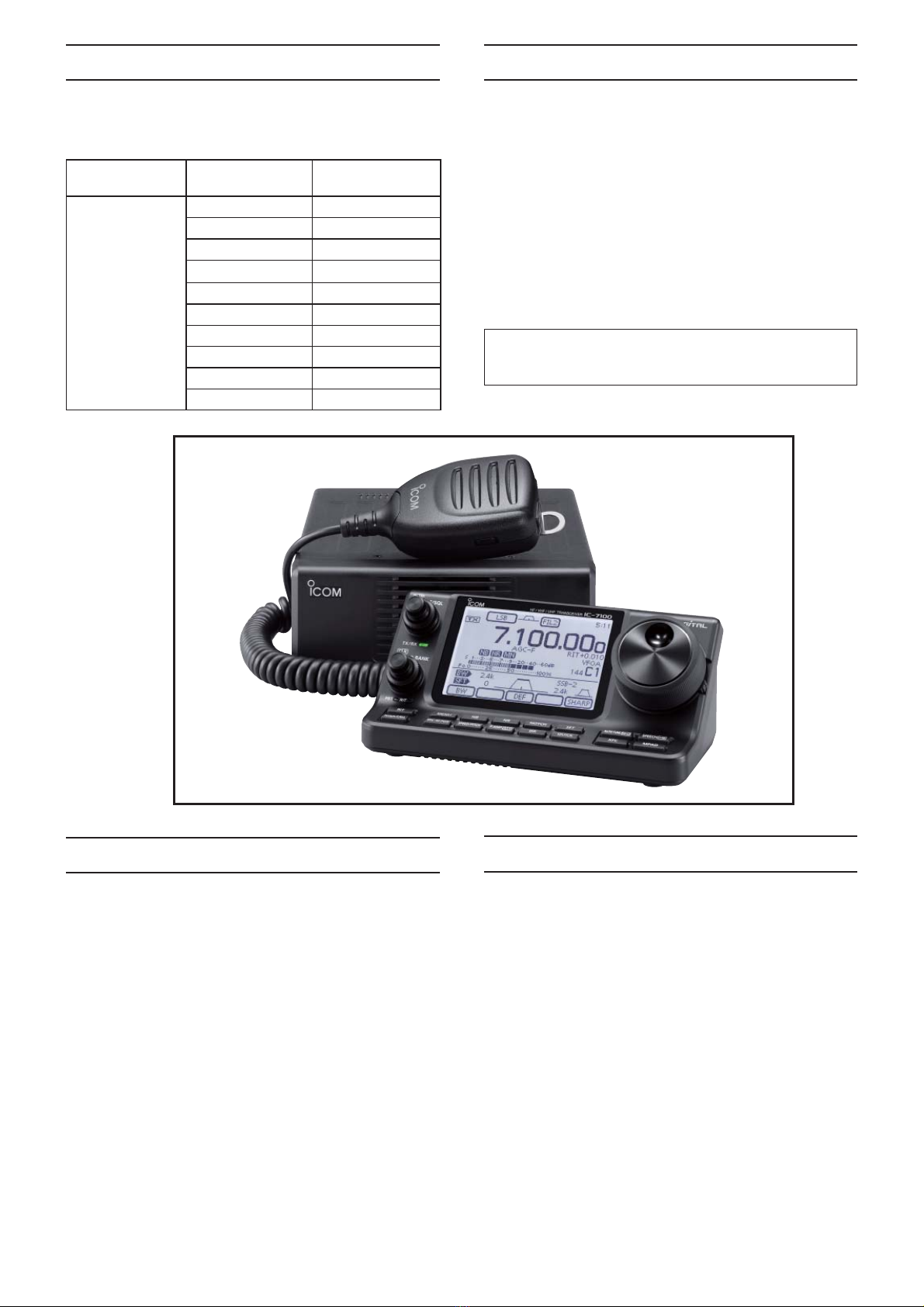
'ENERALD
s&REQUENCYCOVERAGE UNIT-(Z
Receive
0.030000 –199.999999*1*2
400.000000 –470.000000*1*2
Transmit
1.800000 – 1.999999*2, 3.500000 – 3.999999*2,
5.255000 – 5.405000*1*3,
5.332000*3*4, 5.348000*3*4, 5.358500*3*4,
5.373000*3*4, 5.405000*3*4,
7.000000 – 7.300000*2, 10.100000 – 10.150000*2,
14.000000 – 14.350000*2, 18.068000 – 18.168000*2,
21.000000 – 21.450000*2, 24.890000 – 24.990000*2,
28.000000 – 29.700000*2,50.000000 – 54.000000*2,
70.000000 – 70.500000*2, 144.000000 – 148.000000*2,
430.000000 –450.000000*2
*
1Some frequency ranges are not guaranteed.
*
2Depending on version. *3USA version only.
*
4Center frequency.
s-ODE 53",3"#72449!-&-
WFM (RX only), DV
s.OOFMEMORYCHANNELS #((99CH × 5 bank)
s.OOFSCANEDGEMEMORYCHANNELS
6 CH (2 × 3 edges)
s.OOFCALLCHANNELS #((2 × 2 band)
s!NTENNACONNECTOR 3/×2
sAntenna impedance: 50 ø
s5SABLETEMPERATURERANGE
–10˚C to +60˚C;
+14˚F to +140˚F
s&REQUENCYSTABILITY ,ESSTHANÒPPMMINUTES
after power ON. (0˚C to +50˚C;
+32˚F to +122˚F at 430 MHz band)
s&REQUENCYRESOLUTION (Z
s0OWERSUPPLY 6$#Ò
(negative ground)
s0OWERCONSUMPTION
Transmit
Max. power: 22.0 A
Receive
Standby: 0.9 A
Max. audio: 1.2 A
s$IMENSIONSPROJECTIONSNOTINCLUDED
Main unit: 167(W) ×58(H) ×225(D) mm;
6.6(W) ×2.3(H) ×8.9(D) in
Controller: 165(W) ×64(H) ×78.5(D) mm;
6.5(W) ×2.5(H) ×3.1(D) in
s7EIGHTAPPROXIMATELY
Main unit: 2.3 kg; 5.1 lb
Controller: 0.5 kg; 1.1 lb
s!##CONNECTOR PIN
s$!4!CONNECTOR CONDUCTORDMM1⁄10″)
s$!4!CONNECTOR PIN
s2%-/4%CONNECTOR CONDUCTORDMM1⁄8″)
TransmitterD
s/UTPUTPOWER(at 13.8 V DC/+25˚C): (continuously adjustable)
&REQUENCYBAND /UTPUTPOWER
HF/50 MHz 2 to 100 W (AM: 1 to 30 W)*
70 MHz 2 to 50 W (AM: 1 to 15 W)*
144 MHz 2 to 50 W
430 MHz 2 to 35 W
* In the AM mode, transmission can be performed only on
the HF/50/70 MHz frequency band.
s-ODULATIONSYSTEM
SSB: Digital PSN modulation
AM: Digital Low power modulation
FM: Digital Phase modulation
DV: GMSK Digital Phase modulation
s3PURIOUSEMISSION
(Spurious domain)
HF bands: Less than –50 dB
50 MHz band: Less than –63 dB
70/144/430 MHz bands:
Less than –60 dB
(Out-of-band domain)
HF bands: Less than –40 dB
50/70/144/430 MHz bands:
Less than –60 dB
s#ARRIERSUPPRESSION -ORETHAND"
s5NWANTEDSIDEBANDSUPPRESSION
More than 50 dB
s-ICROPHONECONNECTOR PINMODULARJACK
s-ICROPHONEIMPEDANCE ø
s%,%#+%9CONNECTOR CONDUCTORDMM1⁄8″)
s+%9CONNECTOR CONDUCTORDMM1⁄8″)