Icom IC-718 User manual

S-13701MZ-C1
© 2000 Icom Inc.
6-9-16, Kamihigashi, Hirano-ku, Osaka 547-0002, Japan
Count on us!
HF TRANCEIVER
iC-718
iC-718

REPAIR NOTES
1. Make sure a problem is internal before disassembling the
transceiver.
2. DO NOT open the transceiver until the transceiver is
disconnected from its power source.
3. DO NOT force any of the variable components. Turn
them slowly and smoothly.
4. DO NOT short any circuits or electronic parts. An
insulated tuning tool MUST be used for all adjustments.
5. DO NOT keep power ON for a long time when the
transceiver is defective.
6. DO NOT transmit power into a signal generator or a
sweep generator.
7. ALWAYS connect a 50 dB or 60 dB attenuator between
the transceiver and a deviation meter or spectrum analyser
when
using such test equipment.
8. READ the instructions of test equipment thoroughly
before connecting equipment to the transceiver.
To upgrade quality, all electrical or mechanical parts
and internal circuits are subject to change without
notice or obligation.
DANGER
NEVER connect the transceiver to an AC outlet or to a DC
power supply that uses more than 16 V. This will ruin the
transceiver.
DO NOT expose the transceiver to rain, snow or any liq-
uids.
DO NOT reverse the polarrities of the power supply when
connecting the tranceiver.
DO NOT apply an RF signal of more than 20 dBm (100
mW) to the antenna connector. This could damage the
transceiver’s front end.
ORDERING PARTS
Be sure to include the following four points when ordering
replacement parts:
1. 10-digit order numbers
2. Component part number and name
3. Equipment model name and unit name
4. Quantity required
<SAMPLE ORDER>
1110001810 S.IC TA7368F IC-718 MAIN UNIT 1 piece
8810009650 Screw FH BT M3 ×8 NI-ZU IC-718 CHASSIS 6 pieces
Addresses are provided on the inside back cover for your
convenience.
INTRODUCTION
This service manual describes the latest service information
for the IC-718 HF TRANCEIVER at the time of publication.
MODEL
IC-718
VERSION
U.S.A.
Europe
Italy
France
Spain
Other
Korea
U.S.A.
SYMBOL
USA
EUR
ITA
FRA
ESP
OTH
KOR
USA-1
6-9-16, Kamihigashi, Hirano-ku, Osaka 547-0002, Japan
Phone : 06 6793 5302
Fax : 06 6793 0013
URL : http://www.icom.co.jp/world/index.html
Communication Equipment
Himmelgeister Str. 100, D-40225 Düsseldorf, Germany
Phone: 0211 346047 Fax : 0211 333639
URL : http://www.icomeurope.com
Unit 9, Sea St., Herne Bay, Kent, CT6 8LD, U.K.
Phone: 01227 741741 Fax : 01227 741742
URL : http://www.icomuk.co.uk
Zac de la Plaine, Rue Brindejonc des Moulinais
BP 5804, 31505 Toulouse Cedex, France
Phone: 561 36 03 03 Fax : 561 36 03 00
URL : http://www.icom-france.com
Crta. de Gracia a Manresa Km.14,750
08190 Sant Cugat del Valles Barcelona, SPAIN
Phone : (93)590 26 70 Fax : (93)589 04 46
URL : http://www.icomspain.com
<
Corporate Headquarters
>
2380 116th Avenue N.E., Bellevue, WA 98004, U.S.A.
Phone : (425)454-8155 Fax : (425)454-1509
URL : http://www.icomamerica.com
<
Customer Service
>
Phone : (425)454-7619
Glenwood Centre #150-6165
Highway 17 Delta, B.C.,V4K 5B8, Canada
Phone : (604)952-4266 Fax : (604)952-0090
URL : http://www.icomcanada.com
A.C.N.006 092 575
290-294 Albert Street, Brunswick, Victoria, 3056, Australia
Phone: 03 9387 0666 Fax : 03 9387 0022
URL : http://www.icom.net.au
6F No.68, Sec.1 Cheng-Teh Road, Taipei, Taiwan, R.O.C.
Phone: (02) 2559 1899 Fax :(02) 2559 1874

TABLE OF CONTENTS
SECTION 1 SPECIFICATIONS
SECTION 2 INSIDE VIEWS
SECTION 3 DISASSEMBLY INSTRUCTIONS
SECTION 4 CIRCUIT DESCRIPTION
4 – 1 RECEIVER CIRCUITS ................................................................................................................... 4 – 1
4 – 2 TRANSMITTER CIRCUITS ............................................................................................................ 4 – 4
4 – 3 PLL CIRCUIT ................................................................................................................................. 4 – 5
4 – 4 LOGIC CIRCUITS .......................................................................................................................... 4 – 6
4 – 5 REGULATOR CIRCUITS................................................................................................................ 4 – 6
SECTION 5 ADJUSTMENT PROCEDURES
5 – 1 PREPARATION BEFORE SEVICING............................................................................................. 5– 1
5 – 2 PLL ADJUSTMENTS....................................................................................................................... 5 – 2
5 – 3 TRANSMITTER ADJUSTMENTS...................................................................................................5–4
5 – 4 RECEIVER ADJUSTMENTS .......................................................................................................... 5 – 8
5 – 5 SET MODE ADJUSTMENT ............................................................................................................ 5 – 6
SECTION 6 PARTS LIST
SECTION 7 MECHANICAL PARTS AND DISASSEMBLY
SECTION 8 SEMI-CONDUCTOR INFORMATIONS
SECTION 9 BOARD LAYOUTS
9 – 1 MAIN UNIT ..................................................................................................................................... 9 – 1
9 – 2 PLL UNIT ........................................................................................................................................ 9 – 2
9 – 3 LOGIC UNIT ................................................................................................................................... 9 – 3
9 – 4 PHONE BOARD.............................................................................................................................. 9 – 3
9 – 5 MIC BOARD.................................................................................................................................... 9 – 3
9 – 6 VR BOARD ..................................................................................................................................... 9 – 3
9 – 7 FILTER UNIT................................................................................................................................... 9 – 5
9 – 8 PA UNIT .......................................................................................................................................... 9 – 7
SECTION 10 BLOCK DIAGRAM
SECTION 11 WIRING DIAGRAM
SECTION 12 VOLTAGE DIAGRAMS

SECTION 1 SPECIFICATIONS
1 - 1
■GENERAL
• Frequency coverage :
Receive 0.030–29.999999 MHz*1
Transmit 1.800–1.999 MHz*23.500–3.999 MHz*2
7.000–7.300 MHz 10.100–10.150 MHz
14.000–14.350 MHz 18.068–18.168 MHz
21.000–21.450 MHz 24.890–24.990 MHz
28.000–29.700 MHz
*1Guaranteed range: 0.5–29.999999 MHz.
*2Varies accoding to version.
• Mode : USB, LSB, CW, AM, RTTY (FSK)
• No. of memory Ch. : 101 (99 regular, 2 scan edges)
• Freq. resolution : 1 Hz
• Frequency stability : Less than ±200 Hz from 1 min. to
60 min. after power ON. After that
rate of stability less than ±30 Hz/hr
at +25˚C (+77˚F). Temperature
fluctuations 0˚C to 50˚C (+32˚F to
+122˚F) less than ± 350 Hz.
•
Power supply requirement
: 13.8 V DC ±15 %
(negative ground)
• Current consumption :
Transmit max. power 20.0 A
Receive stand-by 1.3 A
max. audio 2.0 A
• Usable temp. range : –10˚C to +60˚C (14˚F to 140˚F)
• Antenna connector : SO-239 (50 Ω)
• Dimensions : 240 (W) ✕95(H) ✕239(D) mm
(projection not included) 97⁄16(W) ✕33⁄4(H) ✕913⁄32(D) in
•Weight : 3.8 kg (8 lb 6 oz)
•ACC connector : 13-pin
•REMOTE connector : 2-conductor 3.5(d) mm (1⁄8")
■TRANSMITTER
•Modulation system :
SSB Balanced modulation
AM Low level modulation
•Output power :
SSB/CW/RTTY/FM 2–100 W
AM 2–40 W
•Spurious emission : Less than –50 dB below peak out-
put power
* spurious frequency ; below 30 MHz: –50 dB,
above 30 MHz: –60 dB
•Carrier suppression : More than 40 dB
•Unwanted sideband suppression:
More than 50 dB
•Mic. connector : 8-pin connector (600 Ω)
•KEY connector : 3-conductor 6.5(d) mm (1⁄4")
•SEND connector : Phono (RCA)
•ALC connector : Phono (RCA)
■RECEIVER
•Receive system : Double-conversion
superheterodyne
•Sensitivity (10 dB S/N) :
SSB, CW, RTTY 0.16 µV*1(1.8–29.999999 MHz)
AM 13 µV (0.5–1.799999 MHz)
2.0 µV*1(1.8–29.999999 MHz)
*1Pre-amp 1 ON
•Squelch sensitivity : Less than 5.6 µV (SSB)
•Selectivity :
SSB, CW, RTTY More than 2.1 kHz/–6 dB
Less than 4.5 kHz/–60 dB
AM More than 6.0 kHz/–6 dB
Less than 20.0 kHz/–40 dB
•Spurious and image rejection ratio:
More than 70 dB
(1.8–29.999999 MHz)
•Audio output power : More than 2.0 W
(at 13.8 V DC)
at 10 % distortion with an 8 Ωload
•RIT variable range : ±1200 Hz
•PHONES connector : 3-conductor 6.5(d) mm (1⁄4")
•EXT SP connector : 2-conductor 3.5(d) mm (1⁄8") 8 Ω
All stated specifications are subject to change without notice or obligation.

2 - 1
SECTION 2 INSIDE VIEWS
Filter unitPA unit
MAIN unit
PLL unit
¡Top view (PA AND FILTER UNITS)
¡Bottom view (MAIN AND PLL UNITS)
Rx RF preamplifier
(Q1401, Q1402: 2SK2171)
Tx Mixer
(Q101, Q102: 3SK131)
1st Lo amplifier
(Q201: 2SC4673)
Rx 1st mixer circuit
(64.455 MHz)
DDS gate allay IC
(IC6: SC-1245A) Reference oscillator circuit
(Q9: 2SC2714,
X1: CR-337, 32.000 MHz)
+5V Reg.
(IC1:TA7805)
BFO DDS
(IC2: SC-1287)
Rx 1st IF amplifier
(Q1201: 3SK131)
2nd mixer circuit
(D401: HSB88WSTR,
Rx; 455 kHz, Tx; 64.455 kHz)
Predrive amplifier
(Q1: 2SC1971) Tx/Rx switching relay
(RL13: AG201344)
Drive amplifier
(Q2, Q3: 2SC3133)
Power amplifier
(Q4, Q5: 2SC2904)
Tx 1st IF amplifier
(Q151: 2SK882)
MIC amplifier
(IC2201: µPC5023)
Tx 455 kHz Modulator
(IC2301: MC1495)
USB, LSB, CW, RTTY filter
(FI611: FL-65)
Rx 2nd IF amplifier
(Q1301: 3SK131)
Tx 2nd IF amplifier
(Q502: 2SK882)
FAN control-2
(Q3601: 2SD1664)
FAN control-1
(IC2101: NJM2058M)
SWR detector
(L13: LR-391)
Tx low-pass filters
(L13: LR-391)

3 - 1
SECTION 3 DISASSEMBLY INSTRUCTIONS
• Removing the covers
Remove 14 screws from the top and bottom covers.
• Removing the Front unit
Remove 4 screws from the front panel.
• How to connect the coaxial cable
Connect the coaxial cable as shown in below.
J6
J3
to MAIN unit
PA unit
FILTER
unit
J1
J701
MAIN unit
PLL unit
J3
from FILTER unit
J6
from PA unit
J701 J1

SECTION 4 CIRCUIT DESCRIPTION
4 - 1
4-1 RECEIVER CIRCUITS
4-1-1 RF SWITCHING CIRCUIT
(FILTER AND MAIN UNITS)
The RF switching circuit leads receive signals to bandpass
filters from the antenna connector while receiving. While
transmitting, this circuit leads signals from the RF power
amplifier to the antenna connector. This circuit includes a 20
dB RF attenuator circuit to prevent distortion from very
strong signals.
RF signals from the antenna connector pass through the
transmit/receive switching relay (RL13), and low-pass filter
(L14, C14–C16), and are then applied to the MAIN unit via
J3 (MAIN unit; J701).
The signals from the FILTER unit are either bypassed or are
attenuated at the 20 dB attenuator (D701, R703). The sig-
nals are then applied to RF filters.
4-1-2 RF BANDPASS FILTER CIRCUIT
(MAIN UNIT)
RF bandpass filters pass only the desired band signals and
suppress any undesired band signals.
The RF circuit has 7 RF bandpass filters (BPF) for signals
above 1.6 MHz and 1 low-pass filter (LPF) for signals and
suppress any undesired band signals.
(1) 0.03–1.6 MHz
The signals pass through the low-pass filter (L821, L822,
C822–C824) to suppress unwanted frequencies. The fil-
tered signals are bypassed a pre-amplifier by a BPF control
signal (B0) and preamp control signal (PROF), and are then
applied to the 1st mixer circuit (Q1101–Q1104).
(2) 1.6–2.0 MHz
The signals pass through a bandpass filter (L831–L833,
L835, L836, C831–C834, C837–C840) to suppress unwant-
ed frequencies. The filtered signals are then applied to the
pre-amplifier circuit.
(3) 2.0–30.0 MHz
The signals pass through a high pass filter (L811–L814,
C811–C817) to suppress excessively strong signals below
2.0 MHz, such as from broadcasting stations. The filtered
signals are applied to a low-pass filter and one of 5 band-
pass filters depending on their frequencies and are then
applied to the pre-amplifier circuit.
4-1-3 PRE-AMPLIFIER CIRCUIT (MAIN UNIT)
The pre-amplifier circuit uses two 2SK2171s to obtain 10 dB
of gain over a wideband frequency range. When the pream-
plifier is turned ON, the signals above 1.6 MHz are applied
to the pre-amplifier circuit.
Q1401 and Q1402 are connected in parallel to easily match
the impedance to 50 Ω. IC3003 (pins 11, 12) switches the
signals from a bandpass filter, either to be bypassed, or to
be applied to the pre-amplifier, depending on the [PREAMP]
switch condition.
Amplified or bypassed signals are applied to the 1st mixer
circuit (Q1102–Q1104)
4-1-4 1ST MIXER CIRCUIT (MAIN UNIT)
The 1st mixer circuit mixes the receive signals with the 1st
LO signal to convert the receive signal frequencies to a
64.455 MHz 1st IF signal.
•Used RF filter
Band
0.03–1.6 MHz
1.6–2 MHz
2–4 MHz
4–8 MHz
Band
8–11 MHz
11–15 MHz
15–22 MHz
22–30 MHz
Control
signal
B4
B5
B6
B7
Control
signal
B0
B1
B2
B3
Input
diode
D8021⁄2
D8021⁄2
D803
D810
Input
diode
D804
D811
D805
D812
• RECEIVER CONSTRUCTION
ANT
1st mixer
Q1101–Q1104 FI301A/B
BFO
2nd LO
1st LO
Crystal
filter
2nd mixer
D401 IC2001
64.455 MHz
SSB, CW, RTTY
Ceramic
BPF
455 kHz
Ceramic
BPF AF
selector
AM
detector
to AF amplifier
SQL controll
AM
FI611
SSB-N,
CW-N,
RTTY-N
(OPTION)
Crystal
BPF

4 - 2
The signals from the pre-amplifier circuit, or signals which
bypass the pre-amplifier, pass through a low-pass filter
(L902, L903, C902–C907). This low-pass filter suppresses
signals above 30 MHz to eliminate direct receiving of signals
at 64.455 MHz and image interference at 130–160 MHz.
The signals are then applied to the 1st mixer
(Q1102–Q1104).
The 1st LO signal (64.485–94.455 MHz) enters the MAIN
unit from the PLL unit via J201 (PLL unit; J4). The LO signal
is amplified at Q201 and then applied to the 1st mixer.
The 1st mxer (Q1101–Q1104) uses four 2SK1740s to pro-
duce high level mixing with a high intercept point.
4-1-5 1ST IF CIRCUIT (MAIN UNIT)
The 1st IF circuit filters and amplifies the 1st IF signals. The
1st IF signals from the 1st mixer circuit are applied to MCF
(Monolithic Crystal Filter: Fl301) to suppress out-of-band
signals. The passband width of FI301 is ±7.5 kHz/–6 dB.
The filtered signals are applied to the 1st IF amplifier
(Q1201). AGC voltage is supplied to the 2nd gate of Q1201.
4-1-6 2ND MIXER CIRCUIT (MAIN UNIT)
The 2nd mixer circuit mixes the amplified 1st IF signals and
2nd LO signal (64.00 MHz) to convert the 1st IF signals into
a 2nd IF signal.
The amplified 1st IF signals from Q1201 are converted into
455 kHz 2nd IF signal at the 2nd mixer (D401). D401 is a
DBM (Double Balanced Mixer). The 2nd LO level is approx.
0 dBm.
The 2nd IF signals are applied to FI1301 to suppress unde-
sired signals such as the 2nd LO signal, and are then
applied to the NB circuit.
4-1-7 NOISE BLANKER CIRCUIT (MAIN UNIT)
The noise blanker circuit detects pulse type noise, and turns
OFF the signal line when noise appears.
The 2nd IF signals from FI1301 are applied to the noise
blanker gate (D1301, D1302). A portion of the signals from
FI1301 is amplified at the noise amplifiers (Q1501, Q1502,
Q1503), then detected at the noise detector (D1501). The
detected signal from the noise detector is applied to the
noise blanker control (Q1508, Q1509).
A portion of the detected signals from the noise detector is
applied to the noise AGC circuit (Q1504, Q1505, R1514,
R1519, C1512) to control the bias voltage of the noise
amplifier (Q1501, Q1502).
The threshold level of the noise blanker switch (Q1508) is
set at 0.9 V. When the detected voltage exceeds the thresh-
old level, Q1509 outputs a blanking signal to close the noise
blanker gate (D1301, D1302), depending on the pulse noise
period. When the operating frequency is changed, the “DN_”
signal line becomes “LOW”, turning Q1509 ON through
D1503. In this case, the noise blanker gate prevents PLL
click noise.
4-1-8 2ND IF CIRCUIT (MAIN UNIT)
The signals passed through the noise blanker gate (D1301,
D1302) are amplified at Q1301. AGC voltage is supplied to
the 2nd gate of Q1301.
When SSB, CW or RTTY mode is selected, the amplified
signals pass through FI611 (FL-65). When an optional CW
narrow filter is installed and CW-N mode is selected, the sig-
nals pass through the CW narrow filter. When AM mode is
selected, the signals bypass the 2nd IF filter.
The filters are selected with mode selecting signals
(SSB/CW, AM, CW-N) and the “T8V”voltage line.
The filtered signal is amplified at Q1603–Q1601 to obtain a
detectable level. AGC voltage is supplied to the 2nd gate of
Q1603. Two thermistors (R1612, R1617), connected to the
gate of Q1602, improves the temperature characteristics of
the receiver gain. R1614 adjusts the receiver gain.
While in SSB, CW or RTTY mode, outputs signal from
Q1601 is applied to the product detector (IC2001). In AM
mode, output signals from Q1601 are shared between the
AM detector (D1901) and AGC detector (D1803).
4-1-9 BFO CIRCUIT (PLL UNIT)
BFO (Beat Frequency Oscillator) frequency is used at the
SSB/CW detector and the balanced modulator. The IC-718
uses a DDS IC for the BFO circuit.
Output signals from the DDS IC (IC2) are filtered by the low-
pass filter (L14, L15, C50–C54), and applied to the product
detector (MAIN unit; IC2001) for receive demodulation.
•Exact 2nd IF frequency
Frequency (kHz)
453.5
456.5
454.1
455.0
Mode
LSB
USB
CW
AM, CW-N •BFO frequency in each mode
Mode
LSB
USB
CW
CW-N
AM
Receive
453.5
456.5
454.1
455.0
No output
Transmit
453.5
456.5
455.0
455.0
455.0
Frequency (kHz)
•Exact 1st IF frequency
Frequency (MHz)
64.4535
64.4565
64.4541
64.4550
Mode
LSB
USB
CW
AM, CW-N

4 - 3
4-1-10 SSB/CW DEMODULATOR CIRCUITS
(MAIN UNIT)
In SSB or CW mode, the 2nd IF signal from the IF amplifier
(Q1601) is mixed with the BFO signal from the PLL unit at
the product detector (IC2001) to demodulate the 2nd IF sig-
nal into AF signals. The detected signals (AF) from IC2001
(pin 1) are applied to the AF input mode selector switch
(IC2102).
4-1-11 AM DEMODULATOR CIRCUITS
(MAIN UNIT)
In AM mode, the 2nd IF signal from the buffer amplifier
(Q1601) passes through C1905 and is detected at D1901.
The detected signal (AF) is then applied to the AF input
mode selector switch (IC2102).
4-1-12 AF INPUT MODE SELECTOR SWITCH
(MAIN UNIT)
The AF signal from one of the detector circuits is applied to
theAF input mode selector switch (IC2102). IC2102 consists
of analog switches which are selected with a mode signal
and the squelch control signal. The AF signal is output from
IC2102 (pin 1) and then applied to the AF amplifier circuit.
4-1-13 AGC CIRCUIT (MAIN UNIT)
The AGC (Automatic Gain Control) circuit reduces IF ampli-
fier gain to keep the audio output at a constant level.
The voltage on the AGC line (Q1805, collector) determines
the receiver gain. The voltage is usually set by D1803 and
the resistance ratio of R1812 and R1813.
The 2nd IF signal from the buffer amplifier (Q1601) is detect-
ed at the AGC detector (D1803) and is then applied to the
DC amplifier (Q1805). –5 V is applied to the Q1805 emitter
to activate the AGC line with minus voltage.
When receiving strong signals, the detected voltage
increases and the voltage of the AGC line decreases via the
DC amplifier (Q1805). As the AGC line is used for the bias
voltage of the IF amplifiers (Q1301, Q1201, Q1603), IF
amplifier gain is decreased.
When the strong signal disappears, C1804 and R1809
release theAGC line voltage in CW or RTTY mode to obtain
a fast AGC release time. While in SSB or AM mode, C1803,
C1805, R1808 and C1802, R1807 are connected in parallel
to obtain a appropriate AGC characteristics (middle or slow
AGC release time), respectively.
4-1-14 S-METER CIRCUIT (MAIN UNIT)
The S-meter circuit indicates the relative received signal
strength while receiving by utilizing the AGC voltage which
changes depending on the received signal strength.
The AGC bias voltage (time constant line) is applied to a dif-
ferential amplifier (IC1701, pin 13) where the difference
between the bias and reference voltage is detected.
The S-meter signal is applied to the A/D converter section in
the CPU (LOGIC unit; IC1, pin 1) and the S/RF indicator dis-
plays the relative signal strength.
4-1-15 SQUELCH CIRCUIT (MAIN UNIT)
The squelch circuit mutes audio output when the S-meter
signal is lower than the [SQL] control setting level.
The S-meter signal from IC1701d (pin 14) is applied to the
CPU (LOGIC unit; IC1) to be compared with the threshold
level set by the [SQL] control.
When the S-meter signal is lower than the threshold level,
the CPU outputs control signal to the AF input mode selec-
tor switch (IC2102, pin 5) via the D/A converter (IC3006).
This cuts the AF signal OFF. The CPU also controls turning
OFF the [RX] indicator, and CPU (pin 88) outputs “SQLS”
signal to the [MIC] connector (pin 6) and [ACC] connector
(pin 13).
4-1-16 AF AMPLIFIER CIRCUIT (MAIN UNIT)
The AF amplifier amplifies the AF input signal to a suitable
driving level for the speaker.
The AF signal from the AF input mode selector switch is
applied to theAF pre-amplifier (IC2101a). The CW side tone
signal is also applied to IC2101a.
The amplified signal is applied to the VCA (IC2701), and
then volume controlled AF signal is power-amplified at the
AF power amplifier (IC2901) to drive the speaker. The AF
signal is applied to the speaker.
•AGC CIRCUIT
AGC line
RFGV
(RF/SQL control) AGC
SLOW
RESET
Q1805
8 V
–5 V
D1803
C1815
2nd IF
signal
C1802 R1801Q1802
AGC
MIDDLE AGC
FAST
C1803R1808Q1803
C1808
R1806Q1801
C1813
C1812
C1814
C1804R1819
R1804
R1812
R1814
R1805
D1802
R1813
R1815
R1810
R1803
Meter
amp.
IC1701d
“SM”
AGC det.
S-meter signal
+
–
12 14
13
SCAN
AM
SSB CW/RTTY

4 - 4
4-2 TRANSMITTER CIRCUITS
4-2-1 MICROPHONE AMPLIFIER CIRCUIT
(FRONT AND MAIN UNITS)
The microphone amplifier circuit amplifies microphone-input
signals and outputs the amplified signal to the balanced
modulator.
Audio signals from the [MIC] connector are applied to the
MIC amplifier IC (IC2201). IC2201 consists of the micro-
phone amplifier, microphone gain control, speech compres-
sor and VOX function. External modulation input from the
[ACC] socket (pin 11) is also applied to IC2201. The micro-
phone bias voltage is supplied from the 8V line via R2225
and R2201.
In AM mode, the ALC circuit (IC2351b, D2381) limits maxi-
mum level of the IC2201 output. The maximum modulation
level is set by R2385 (MAIN unit).
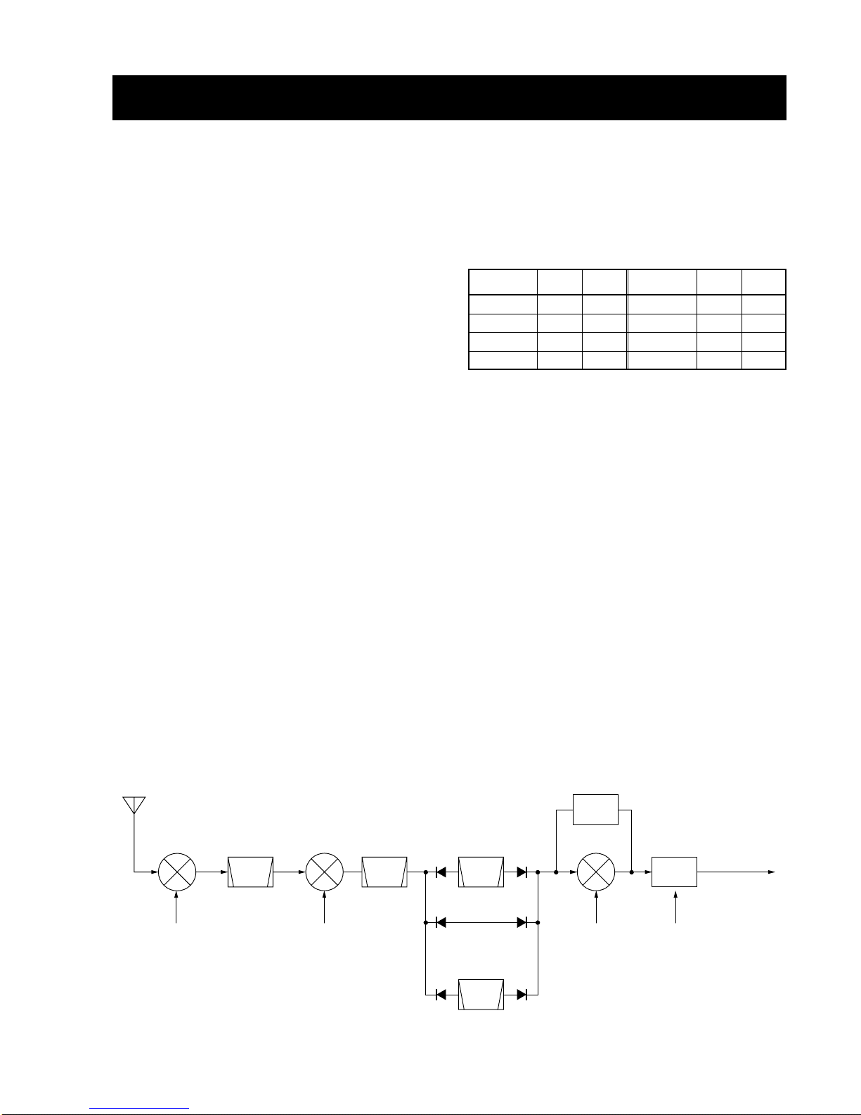
4-2-2 BALANCED MODULATOR (MAIN UNIT)
The balanced modulator converts the AF signal from the
microphone amplifier to a 455 kHz IF signal with a BFO sig-
nal.
Output signals from the microphone amplifier and the CW
keying signal are applied to the balanced modulator
(IC2301, pin 1). The BFO signal from the PLL unit is applied
to IC2301 (pin 10) as a carrier signal.
C2301 is a doubled balanced mixer IC and outputs a double
side band (DSB) signal with –40 dB carrier suppression.
R2303 adjusts the balanced level of IC2301 for maximum
carrier suppression. In CW mode, the CW keying signal
upsets the balance to create a carrier signal. In AM mode,
Q2302 and R2321 upset the balance to create an AM carri-
er signal.
4-2-3 CW KEYING CIRCUIT (MAIN UNIT)
When the CW key is closed, control signal is output from
CPU (LOGIC unit) and controls break-in operation, the side
tone signal.
The input signal (DOT or DAS) from CW keyer is applied to
the CPU (LOGIC unit; IC1, pins 71, 70) and then CPU out-
puts CW control signal (KDS) from pin 77. The CW control
signal is applied to the balanced modulator (IC2301) via
Q3701, Q3702, D3701 to unbalance the IC2301 input bias
voltage and create a carrier signal. R3703 determines the
transmit delay timing.
4-2-4 IF AMPLIFIER (MAIN UNIT)
The SSB/CW/RTTY 455 kHz IF signal passes through FI611
(FL-65) to suppress unwanted sideband signals, then the
signal is applied to a transmit IF amplifier (Q502). The
optional CW narrow filter is not used in transmitting.
The amplified signal from Q502 is mixed with the 2nd LO
signal and converted to a 64.455 MHz IF signal at D401.
D401 is used in receiving and transmitting. The AM signal
bypasses FI611, and is amplified at Q502 and is then
applied to D401.
The 64.455 MHz IF signal is filtered at FI301, amplified at
the IF amplifier (Q151) and is then converted to the dis-
played frequency at the balanced mixer (Q101, Q102) with
the 1st LO signal.
The gates of the IF amplifiers (Q151, Q502) are controlled
by ALC bias voltage from the ALC circuit. A thermistor
(R508), connected to the gate of Q502, improves the tem-
perature characteristics of the transmitter gain. R503 adjusts
the total transmitter gain.
4-2-5 RF CIRCUIT (MAIN AND PA UNITS)
The displayed frequency signal converted at the balanced
mixer (MAIN unit; Q101, Q102) is applied to the bandpass
filter (L101–L103, C101–C107) where unwanted LO signal
emission is reduced. The filtered signal is attenuated at
R5–R7 and amplified at IC1, and is then applied to the PA
unit via the attenuator (R1–R3).
The signals from the MAIN unit are amplified at the predrive
amplifier (Q1), drive amplifier (Q2, Q3) and power amplifier
(Q4, Q5) in the PA unit to obtain a stable 100 W of RF out-
put power.
The predrive amplifier is a class-A amplifier with a VCC of
13.8 V. The drive amplifier is a class-AB push-pull amplifier
with a VCC of 13.8 V. D1 controls bias voltage to the drive
amplifier.
The impedance of the signal from the drive amplifier is con-
verted at L2, and then the signal is applied to the power
amplifier (Q4, Q5). The power amplifier is a class-AB push-
pull amplifier and amplifies the input signal to 100 W. D2 and
D3 control bias voltage to the power amplifier. The signal
from the power amplifier is applied to one of the low-pass fil-
ters in the FILTER unit.
4-2-6 LOW-PASS FILTER CIRCUIT (FILTER UNIT)
The low-pass filter circuit consists of 6 Chebyschev low-
pass filters to suppress the higher harmonic components.
The signal from the power amplifier (Q4, Q5) is applied to
one of the low-pass filters (depending on its frequency). The
filter switching voltage from the MAIN unit (J4001) is applied
to the FILTER unit via J1.
The filtered signal passes through the SWR detector circuit
(L13) and is then applied to the antenna connector.
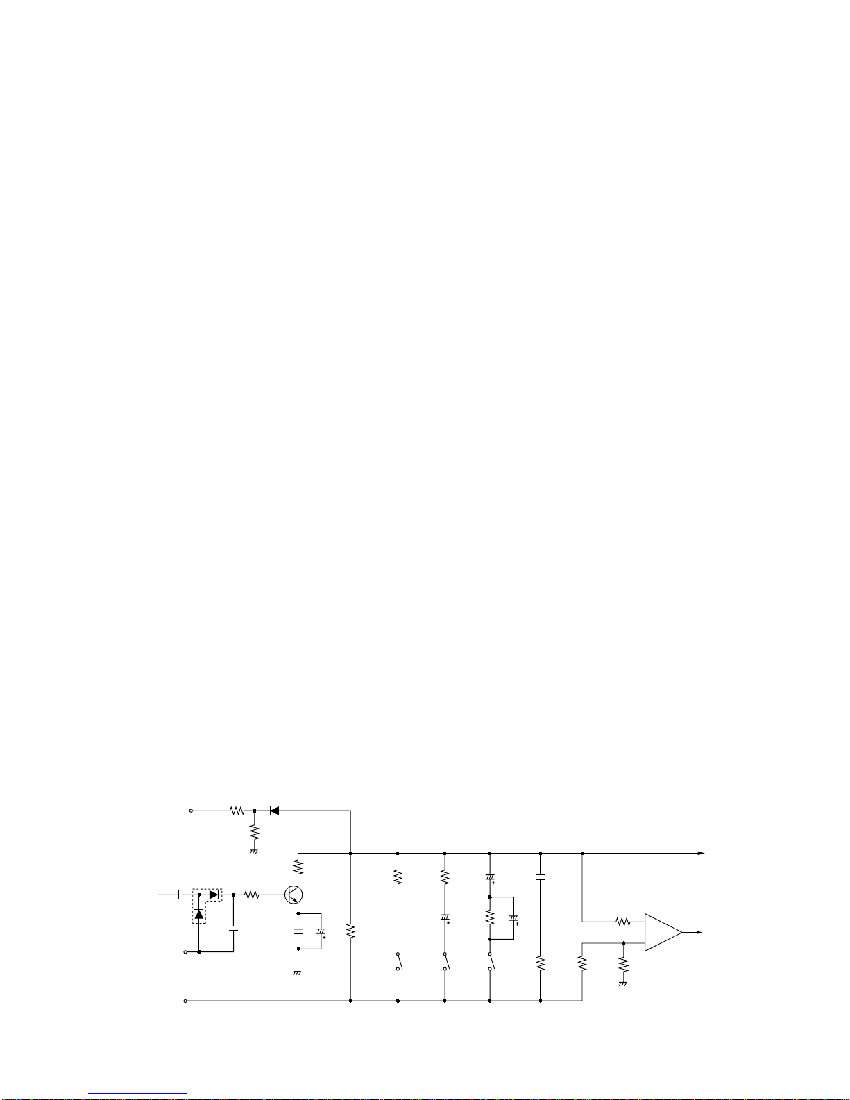
4-2-7 ALC CIRCUIT (MAIN UNIT)
The ALC (Automatic Level Control) circuit controls the gain
of IF amplifiers in order for the IC-718 to output a constant
RF power set by the [RF PWR] control even when the sup-
plied voltage shifts, etc.
The “FOR”voltage from the FILTER unit is applied to
IC1701c (pin 9) in the MAIN unit. The “POCV”voltage from
the D/A converter (IC3301, pin 2), determined by the RF
power setting, is applied to IC1701c (pin 10) as the refer-
ence voltage.

4 - 5
When the “FOR”voltage exceeds the “POCV”voltage, ALC
bias voltage from IC1701c (pin 8) controls the IF amplifiers
(Q151, Q502). This adjusts the output power to the deter-
mined level by the RF power setting until the “FOR”and
“POCV”voltages are equalized.
In AM mode, Q1705 turns ON and C1707, C1708 are con-
nected to the “FOR”voltage line to obtain an averaging ALC
operation. Q1706 turns ON and the “POCV”voltage is shift-
ed for 40 W AM output power (maximum) through R1730.
An external ALC input from the [ACC] socket or the [ALC]
jack is applied to the buffer amplifier (Q1703). External ALC
operation is identical to that of the internal ALC.
4-2-8 APC CIRCUIT (MAIN UNIT)
The APC (Automatic Power Control) circuit protects the
power amplifiers on the PA unit from high SWR and exces-
sive current.
Areflected wave signal appears and increases on the anten-
na connector when the antenna is mismatched. D3 of the
SWR detector circuit (L13, D2, D3) in the FILTER unit
detects the signal and applies it to IC1701b in the MAIN unit
as the “REF”signal. When the “REF”signal level increases,
IC1701b decreases the ALC line voltage via R1716 to acti-
vate the ALC.
For the currentAPC, the power transistor current is obtained
by detecting the voltage (“ICH”and “ICL”) which appear at
both terminals of a 0.012 Ωresistor (PA unit; R25). The
detected voltage is applied to the differential amplifier
(IC1701a, pins 2, 3). When the current of the final transistors
is more than 22 A, IC1701a controls the ALC line via D1705
to prevent excessive current flow.
During tuning of an antenna with an optional AH-4, The
“PODN”signal turns Q51 ON. As a result, the “POCV”volt-
age is shifted for approx. 10 W output power.
4-2-9 TEMPERATURE PROTECTION CIRCUIT
(MAIN UNIT)
A cooling fan (CHASSIS; MF1) is activated while transmit-
ting or if the temperature of Q4 (PA unit) exceeds the preset
value.
While transmitting, PAT8 voltage is provided to MF1 via R30.
Thermistor R30 on the PA unit detects the temperature of
Q4. If the Q4 temperature is more than 50˚C (122˚F), R30
becomes very low impedance. Then TEMP signal from PA
unit is applied to the A/D converter section of the CPU (IC1,
pin 92) in the LOGIC unit as PATL signal. And the CPU out-
puts control signal to rotate the cooling fan at high speed via
the I/O expander (IC3301)–even when the transceiver con-
dition has changed from transmit to receive.
4-2-10 RF METER CIRCUIT (MAIN UNIT)
The “FOR”voltage from the FILTER unit is applied to the RF
meter amplifier (IC1751a, pin 2) via the ALC amplifier
(IC1701c). The amplified voltage is output from IC1751a (pin
1) and then applied to the A/D converter section of the CPU
(IC1, pin 99) in the LOGIC unit.
4-3 PLL CIRCUITS
4-3-1 GENERAL DESCRIPTION
The PLL unit contains 2 DDS circuits for generating a 1st LO
signal (64.485–94.455 MHz variable) and a BFO frequency
(453.5–456.5 kHz). The 1st LO PLL employs a 1 loop DDS
PLL whose reference oscillator is also used as the 2nd LO
signal (64.00 MHz fixed). The DDS (Direct Digital
Synthesizer) circuit performs signal-sampling, generation of
digital sine wave and digital phase detection.
4-3-2 1ST LO CIRCUIT (PLL UNIT)
The PLL contain one VCO circuit (Q18, D4) for all HF band
coverage within 1 Hz step. The VCO oscillation signal is
buffer-amplified at Q26 and is then amplified at Q29, Q32
and Q30. The resulting signal is applied to the DDS IC (IC6).
The DDS IC outputs pulse-type signals. The signals are
applied to the loop filter to be converted into DC voltage
(lock voltage).
The lock voltage is applied to the varactor diode (D4) in the
VCO circuit to change the capacitance of this diode and con-
trol the oscillation frequency.
The VCO oscillating signal is then buffer-amplified at the
buffer amplifier (Q26), amplified at Q28, and finally applied
to the MAIN unit as a 1st LO signal.
•ALC CIRCUIT
REF voltageFOR voltage
EALC
(external ALC)
ALC
8V
14V
AMS
–5V
Q1705
C1744
R1725 R1724
R1706
D1706
D1707
D1701 D1703
D1702
D1704
Q1703
R1712R1729
C1707
C1706
R1714 R1716
R1713
Q1706
IC3301
ALC
amp.
IC1701b
–
+
57
6
R1709
R1708
R1703 POCV line
R1730
R1711
R1710
ALC
amp.
IC1701C
–
+
92 8
10 4
11
D/A
converter
R1707
RF power
setting

4 - 6
4-3-3 REFERENCE OSCILLATOR CIRCUIT
(PLL UNIT)
The reference oscillator circuit consists of Q9 and X1. A
32.00 MHz reference frequency is oscillated to produce a
2nd LO signal, DDS reference frequency and BFO DDS
clock signal.
The 32.00 MHz reference frequency is doubled at Q10 to
obtain the 2nd LO signal. The resulting 64.00 MHz signal is
filtered at the bandpass filter and is then applied to the MAIN
unit via J1 as the 2nd LO signal.
4-4 LOGIC CIRCUITS
4-4-1 BAND SELECTION DATA (MAIN UNIT)
To selection the correct bandpass filter and low-pass filter,
the CPU outputs the following band selection data from the
I/O expander (MAIN unit; IC3001) depending on the dis-
played frequency.
4-4-2 RIT CONTROL (FRONT UNIT)
The [RIT] control shifts the “RIV”voltage in order to shift the
receive frequency. The voltage is applied to the A/D con-
verter section of the CPU (IC1, pin 1). The CPU shifts the N-
data for the DDS IC.
4-4-3 CPU (LOGIC UNIT)
The CPU (IC1) contains an 8-bit CMOS CPU, a 60 k-byte
ROM, a 2 k-byte RAM. A 9.8304 MHz clock is used for rapid
operation. The CPU controls the operating frequency, mode,
function display, etc. The memory channel information is
stored in the EEPROM (IC2).
The Icom CI-V network system allows the IC-718 to be
remotely controlled by a personal computer using an RS-
232C I/O port.
4-5 REGULATOR CIRCUITS
Either +8 V, +5 V or –5 V DC is supplied from a corre-
sponding regulator circuit. +8 V, +5 V and –5 V DC are reg-
ulated at the following circuits using 13.8 V DC.
(1) +5 V REGULATOR (FRONT UNIT)
+ 5 V DC is provided by a three-terminal voltage regulator
(IC4).
(2) + 8 V REGULATOR (MAIN UNIT)
+ 8 V DC is provided by a three-terminal voltage regulator
(IC17).
(3) –5 V REGULATOR (MAIN UNIT)
IC16 generates a negative pulse-type voltage by converting
the DC input to AC voltage (approx. 6.7 kHz) as a multi-
vibrator. The voltage is rectified at D80 and D81, regulated
by a Zener diode (D82) and C249, and is then applied to the
MAIN and PLL units.
•FREQUENCY CONSTRUCTION
64.485–
97.455 MHz 453.3–
456.5 kHz
64.0 MHz
ANT 1st mixer
Q1101–Q1104
IC2
Q10
BFO2nd LO1st LO
PLL unit
MAIN unit
DDS
DDS
Crystal
filter
2nd mixer
D401 Demodulator
64.455 MHz
BPF
455 kHz to AF circuit
Reference
oscillator
X1: 32.0 MHz Q9
IC6
Q18
LPF
✕2
BPF
Loop
filter
BPF
•Band selection data
Band
0.03–1.59999 MHz
1.6–1.99999 MHz
2.0–3.99999 MHz
4.0–7.99999 MHz
8.0–10.99999 MHz
11.0–14.99999 MHz
15.0–21.99999 MHz
22.0–30.00000 MHz
Band
voltage
7.4 V
6.0 V
5.0 V
0 V
4.0 V
3.1 V
2.2V
BPF
B0
B1
B2
B3
B4
B5
B6
B7
LPF
L1
L2
L3
L4
L5
L6

SECTION 5 ADJUSTMENT PROCEDURES
5 - 1
5-1 PREPARATION BEFORE SERVICING
■REQUIRED TEST EQUIPMENT
DC power supply
RF power meter
(terminated type)
Frequency counter
RF voltmeter
Modulation analyzer
Distortion meter
Oscilloscope
Digital multimeter
Spectram analyzer
Standard signal
generator (SSG)
AC millivoltmeter
DC voltmeter
DC ammeter
Audio generator
Attenuator
External speaker
Terminator
EQUIPMENT GREDE AND RANGE EQUIPMENT GREDE AND RENGE
Output voltage : 13.8 V DC
Current capacity : 30 A or more
Measuring range : 10–200 W
Frequency range : 1.8–30 MHz
Impedance : 50 Ω
SWR : Less than 1.2 : 1
Frequency range : 0.1–100 MHz
Frequency accuracy : ±0.5 ppm or better
Sensitivity : 100 mV or better
Frequency range : 0.1–100 MHz
Measuring range : 0.01–10 V
Frequency range : At least 30 MHz
Measuring range : 0–100 %
Frequency range : 1 kHz ±10 %
Measuring range : 1–100 %
Frequency range : DC–20 MHz
Measuring range : 0.01–10 V
Imput impedance : 10 MΩ/DC or beter
Frequency range : At least 90 MHz
Spectraum bandwidth : 100 kHz or more
Frequency range : 0.1–100 MHz
Output level : 0.1 µV–32 mV
(–127 to –17 dBm)
Measuring range : 10 mV–10 V
Input impedance :
50 kΩ/V DC or better
Measurement capability: 1 A and 30 A
Frequency range : 300–3000 Hz
Measuring range : 1–500 mV
Power attenuation : 50 or 60 dB
Capacity : 150 W or more
Input impedance : 8 Ω
Capacity : 5 W or more
Resistance : 50 and 150 Ω
Capacity : 150 W or more
‘‘CONNECTIONS
Modulation analyzer
RF power meter
Spectrum analyzer
Attenuator
Distortion meter
DC power supply Ammeter
Standard signal
generator
CAUTION !
DO NOT transmit while
an SSG is connected to
the antenna connector.
to the antenna connector
to [DC 13.8 V]
to [EXT SP]
Speaker
Audio generator
PTT
,.
IC-718
•Microphone connector
(Front panel view)
Pin 1 Pin 7
Pin 6
Pin 5

5 - 2
5-2 PLL ADJUSTMENTS
REFERENCE
FREQUENCY
VCO LOCK
VOLTAGE
1ST LO
OUTPUT
LEVEL
2ND LO
OUTPUT
LEVEL
BFO
OUTPUT
ADJUSTMENT
ADJUSTMENT ADJUSTMENT CONDITION MEASUREMENT VALUE POINT
UNIT LOCATION UNIT ADJUST
1
2
3
1
2
1
2
1
1
2
3
•Display frequency: Any
•Set C16 as illustration at below.
•Receiving
•Display frequency: 29.99999 MHz
•Receiving
•Display frequency: 0.03000 MHz
•Receiving
•Display frequency: 29.99999 MHz
•Mode : USB
•Receiving
•Display frequency: 0.03000 MHz
•Mode : LSB
•Receiving
•Display frequency: 14.10000 MHz
•Mode : USB
•Receiving
•Display frequency: 14.10000 MHz
•Mode : USB
•Receiving
•Mode : AM
•Receiving
PLL
PLL
PLL
PLL
PLL
Connect a frequency
counter to check
point P1.
Connect an RF volt-
meter to check point
P1.
Connect a digital
multimeter or oscillo-
scope to check point
CP1.
Connect an RF volt-
meter to check point
P4.
Connect an RF volt-
meter to check point
P1.
Connect an RF volt-
meter to check point
P5.
Connect a frequency
counter to check
point P5.
64.00000 MHz
Maximum level
4.15 V
More than 0.8 V
–3 dBm to +3dBm
–2 dBm to +4 dBm
–18 dBm to –12 dBm
456.5 kHz
No output
PLL
PLL
L4
L6, L7
C165
Verify
Verify
Verify
Verify
Turn L6, L7 on the PLL unit to downside for
presetting until the frequency counter reads
frequency.
C16
CP1
C16
CP1
VCO lock voltage
check point
•PLL unit (bottom view)

5 - 3
2nd LO
J1
1
2
1
2
P2
BFO
J2
1
2
1st LO
J4
1
2
1
2P3
C7
C6
Reference
OSC level
adjustment
P1 Reference
frequency
check point
C16 Reference
frequency
pre-setting
P4 1st LO
output level
check point
P5
BFO
check point
C165
VCO lock voltage
adjustment
L4
Reference
freauency
adjustment
•PLL unit

5 - 4
5-3 TRANSMITTER ADJUSTMENTS
IDLING
CURRENT
(for driver)
(for final
amplifier)
SWR
DETECTOR
TRANSMITTER
TOTAL GAIN
OUTPUT
POWER
Ic APC
ADJUSTMENT
ADJUSTMENT ADJUSTMENT CONDITION MEASUREMENT VALUE POINT
UNIT LOCATION UNIT ADJUST
1
2
1
2
1
2
1
1
• Display frequency: 14.10000 MHz
• Mode : USB
• RF power : Minimum (L)
• Mic gain : Minimum (0)
• Disconnect J3601 (MAIN unit) and
preset R21, R24 (PA unit) to max.
counter clockwise.
• Transmitting
• Transmitting
• Display frequency: 14.10000 MHz
• Mode : USB
• RF power : Maximum (H)
• Connect J4 (FILTER) unit to GND.
• Connect an audio generator to
[MIC] connector and set as:
Frequency : 1.5 kHz
Level : 30 mVrms
• Transmitting
• Transmitting
• Display frequency: 14.10000 MHz
• Mode : USB
• RF power : Maximum (H)
• Mic gain : Center (50)
•
R2701 (MAIN unit)
: Center
• Connect an audio generator to
[MIC] connector and set as:
Frequency : 1.5 kHz
Level : 3 mVrms
• Transmitting
• Transmitting
• Display frequency: 14.10000 MHz
• Mode : USB
• RF power : Maximum (H)
• MIC gain : Center (50)
• Connect an audio generator to
[MIC] connector and set as:
Frequency : 1.5 kHz
Level : 30 mVrms
• Transmitting
• Display frequency: 3.55000 MHz
• Mode : USB
• Connect CP4002 (MAIN unit) to
GND.
• RF power : Maximum (H)
• Mic gain : Center (50)
• Connect an audio generator to
[MIC] connector and set as:
Frequency : 1.5 kHz
Level : 30 mVrms
• Transmitting
PA
Rear
panel
FILTER
Rear
panel
Rear
panel
Rear
panel
Connect an ammeter
(3 A) between power
supply and the IC-
718.
Connect an RF
power meter to [ANT]
connector.
Connect a digital
multimeter or oscillo-
scope to J5.
Connect an RF
power meter to [ANT]
connector.
Connect an RF
power meter to [ANT]
connector.
Connect an ammeter
(30A) between power
supply and the IC-
718.
At the point where the
Tx current Increases
200 mA.
At the point where the
Tx current Increases
400 mA.
100 W
Minimum voltage
Maximum output
power
50 W
100 W
22 A
PA
Front
panel
FILTER
MAIN
MAIN
MAIN
R21
R24
Mic gain
control in
the quick
set mode
C17
L106,
L151,
L301,
L302,
L303,
L501
R503
R1707
R1720
After adjustment, connect J3601 on the MAIN unit.
After adjustment, disconnect J4 on the FILTER unit from GND.
After adjustment, disconnect CP4002 on the MAIN unit from GND.

5 - 5
CP4002
Ic APC pre-setting
J3601
Idling current
pre-setting
R1707
Output power
adjustment
L151
Tx total gain
adjustment
L106
R503
L501
L303
L302
L301
R1720
Ic APC
adjustment
R2701
Tx total gain
pre-setting
R21
Idling current
adjustment
(Driver)
R24
Idling current
adjustment
(Final)
J5
SWR detector
check point
J4
SWR detector
pre-setting
C17
SWR detector
adjustment
•PA unit •FILTER unit
•MAIN unit

5 - 6
TRANSMITTER ADJUSTMENTS—continued
CARRIER
SUPPRESSION
AM
CARRIER
AM
MODULATION
CW
CARRIER
ADJUSTMENT
ADJUSTMENT ADJUSTMENT CONDITION MEASUREMENT VALUE POINT
UNIT LOCATION UNIT ADJUST
1
1
1
2
1
•Display frequency: 14.10000 MHz
•Mode : USB
•Mic gain : Minimum (0)
•Apply no audio signals to [MIC]
connector.
•Transmitting
•Display frequency: 14.10000 MHz
•Mode : AM
•RF power : Maximum (H)
•Mic gain : Minimum (0)
•
R2321 (MAIN unit)
: Center
•
R2385 (MAIN unit)
: Center
•Apply no audio signals to [MIC]
connector.
•Transmitting
•Display frequency: 14.10000 MHz
•Mode : AM
•RF power : Maximum (H)
•Mic gain : Center (50)
•
R2385 (MAIN unit)
: Center
•Connect an audio generator to
[MIC] connector and set as:
Frequency : 1 kHz
Level : 30 mVrms
•Transmitting
•Set an AG as:
Frequency : 1 kHz
Level : 3 mVrms
•Transmitting
•Display frequency: 14.10000 MHz
•Mode : CW
•RF power : Maximum (H)
•Connect a keyer to the [KEY] jack.
•Key down (transmitting)
Rear
panel
Rear
panel
Rear
panel
MAIN
Connect a spectrum
analyzer to the [ANT]
connector through an
attenuator.
Connect an RF
power meter to [ANT]
connector.
Connect a modula-
tion analyzer to the
[ANT] connector
through an attenua-
tor.
Connect an oscillo-
scope to CP3701 and
[ANT] connector.
Minimum carrier level
40 W
90% modulation
70% modulation
Adjust as follows:
MAIN
MAIN
MAIN
MAIN
R2303
R1730
R2321
Verify
R3703
10 msec.
Keying (CP3701)

5 - 7
CP3701
CW carrier
check point
R3703
CW carrier
adjustment
R1730
AM carrier
adjustment
R2321
AM modulation
adjustment
(or AM carrier pre-setting)
R2385
AM carrier and
AM modulation
pre-setting
R2303
Carrier suppression
adjustment
•MAIN unit

5 - 8
*This output level of a standard signal generator (SSG) is indicated as SSG’s open circuit.
5-4 RECEIVER ADJUSTMENTS
Receiver total gain adjustment must perform after transmitter total gain adjustment.
RECEIVER
TOTAL GAIN
NOISE
BLANKER
ADJUSTMENT
ADJUSTMENT ADJUSTMENT CONDITION MEASUREMENT VALUE POINT
UNIT LOCATION UNIT ADJUST
1
2
1
2
•R2701 (MAIN unit): Center
•Turn R1614 (MAIN unit) to 90˚
counter clockwise from center posi-
tion.
•Display frequency: 14.10000 MHz
•Mode : USB
•[RIT] : OFF (Center)
•[NB] : OFF
•[P.AMP] : ON
•[ATT] : OFF
•Connect an SSG to [ANT] connec-
tor and set as:
Frequency : 14.10150 MHz
Level : 1.0 µV* (–107 dBm)
Modulation: OFF
•Receiving
•[P.AMP] : OFF
•[ATT] : OFF
•Set an SSG as:
Level : 1.0 mV* (–47 dBm)
and OFF
•Receiving
•Display frequency: 14.10000 MHz
•Mode : USB
•[P.AMP] : ON
•[NB] : OFF
•Connect an SSG to [ANT] connec-
tor and set as:
Frequency : 14.10150 MHz
Level : 3.2 µV* (–97 dBm)
Modulation: OFF
and apply following signal to [ANT]
connector.
•Receiving
•[NB] : ON
•Receiving
Rear
panel
MAIN
Connect an AC milli-
volt meter to [EXT
SP] connector with
an 8 Ωload.
Connect an oscillo-
scope to check point
CP1501.
Maximum audio output
level
30 dB of AF level differ-
ence
Maximum noise wave-
form
The noise must be
blanked
MAIN
MAIN
MAIN
L1103,
L1201,
L1202,
L1621,
R1614
L1501,
L1502
Verify
100 msec.
1 msec.
Other manuals for IC-718
10
This manual suits for next models
1
Table of contents
Other Icom Transceiver manuals