Icom IC-F620 User manual

SERVICE
MANUAL
UHF TRANSCEIVER
iF610
iF620
iF621

VERSION
Europe
General
Europe (MPT)
General (MPT)
U.S.A.
U.S.A. (MPT)
U.S.A.
General
SYMBOL
EUR
GEN
MTE
MTG
USA
MTU
USA
GEN
INTRODUCTION
This service manual describes the latest service information
for the IC-F610,IC-F620 and IC-F621 UHF TRANS-
CEIVERS at the time of publication.
DANGER
NEVER connect the transceiver to an AC outlet or to a DC
power supply that uses more than 16 V. This will ruin the
transceiver.
DO NOT expose the transceiver to rain, snow or any liquids.
DO NOT reverse the polarities of the power supply when
connecting the transceiver.
DO NOT apply an RF signal of more than 20 dBm (100 mW)
to the antenna connector. This could damage the transceiv-
er’s front end.
ORDERING PARTS
Be sure to include the following four points when ordering
replacement parts:
1. 10-digit order numbers
2. Component part number and name
3. Equipment model name and unit name
4. Quantity required
<SAMPLE ORDER>
1110003490 S.IC TA31136FN IC-F610 MAIN UNIT 5 pieces
8810009990 Screw PH BT M3×8 ZK IC-F620 Bottom cover 10 pieces
Addresses are provided on the inside back cover for your
convenience.
REPAIR NOTES
1. Make sure a problem is internal before disassembling the
transceiver.
2. DO NOT open the transceiver until the transceiver is
disconnected from its power source.
3. DO NOT force any of the variable components. Turn
them slowly and smoothly.
4. DO NOT short any circuits or electronic parts. An insu-
lated tuning tool MUST be used for all adjustments.
5. DO NOT keep power ON for a long time when the trans-
ceiver is defective.
6. DO NOT transmit power into a signal generator or a
sweep generator.
7. ALWAYS connect a 50 dB to 60 dB attenuator between
the transceiver and a deviation meter or spectrum ana-
lyzer when using such test equipment.
8. READ the instructions of test equipment thoroughly
before connecting equipment to the transceiver.
MODEL
IC-F610
IC-F620
IC-F621
To upgrade quality, any electrical or mechanical parts and
internal circuits are subject to change without notice or
obligation.

TABLE OF CONTENTS
SECTION 1 SPECIFICATIONS
SECTION 2 INSIDE VIEW
SECTION 3 DISASSEMBLY INSTRUCTIONS
SECTION 4 CIRCUIT DESCRIPTION
4 - 1 RECEIVER CIRCUITS . . . . . . . . . . . . . . . . . . . . . . . . . . . . . . . . . . . . . . . . . . . . . . . . . . . . . . . . . . . . 4 - 1
4 - 2 TRANSMITTER CIRCUITS . . . . . . . . . . . . . . . . . . . . . . . . . . . . . . . . . . . . . . . . . . . . . . . . . . . . . . . . 4 - 2
4 - 3 PLL CIRCUITS . . . . . . . . . . . . . . . . . . . . . . . . . . . . . . . . . . . . . . . . . . . . . . . . . . . . . . . . . . . . . . . . . 4 - 3
4 - 4 POWER SUPPLY CIRCUITS . . . . . . . . . . . . . . . . . . . . . . . . . . . . . . . . . . . . . . . . . . . . . . . . . . . . . . . 4 - 4
4 - 5 PORT ALLOCATIONS . . . . . . . . . . . . . . . . . . . . . . . . . . . . . . . . . . . . . . . . . . . . . . . . . . . . . . . . . . . . 4 - 4
SECTION 5 ADJUSTMENT PROCEDURES
5 - 1 PREPARATION . . . . . . . . . . . . . . . . . . . . . . . . . . . . . . . . . . . . . . . . . . . . . . . . . . . . . . . . . . . . . . . . . 5 - 1
5 - 2 PLL ADJUSTMENT . . . . . . . . . . . . . . . . . . . . . . . . . . . . . . . . . . . . . . . . . . . . . . . . . . . . . . . . . . . . . . 5 - 3
5 - 3 SOFTWARE ADJUSTMENT . . . . . . . . . . . . . . . . . . . . . . . . . . . . . . . . . . . . . . . . . . . . . . . . . . . . . . . 5 - 4
SECTION 6 PARTS LIST
SECTION 7 MECHANICAL PARTS
SECTION 8 SEMI-CONDUCTOR INFORMATION
SECTION 9 BOARD LAYOUTS
9 - 1 FRONT UNIT . . . . . . . . . . . . . . . . . . . . . . . . . . . . . . . . . . . . . . . . . . . . . . . . . . . . . . . . . . . . . . . . . . . 9 - 1
9 - 2 MAIN UNIT . . . . . . . . . . . . . . . . . . . . . . . . . . . . . . . . . . . . . . . . . . . . . . . . . . . . . . . . . . . . . . . . . . . . 9 - 3
SECTION 10 BLOCK DIAGRAM
SECTION 11 VOLTAGE DIAGRAMS
11 - 1 FRONT UNIT . . . . . . . . . . . . . . . . . . . . . . . . . . . . . . . . . . . . . . . . . . . . . . . . . . . . . . . . . . . . . . . . . . 11 - 1
11 - 2 MAIN UNIT . . . . . . . . . . . . . . . . . . . . . . . . . . . . . . . . . . . . . . . . . . . . . . . . . . . . . . . . . . . . . . . . . . . 11 - 2
EXPLICIT DEFINITIONS
H1-band
H2-band
400 –430 MHz
440 –490 MHz
480 –512 MHz
480 –520 MHz
L-band
M-band
H-band
FREQUENCY COVERAGE
12.5 kHz / 25 kHz
12.5 kHz / 20 kHz
Narrow/Wide-type
Narrow/Middle-type
CHANNEL SPACING

1 - 1
SECTION 1 SPECIFICATIONS
Measurement method
Frequency coverage
Type of emission
Number of conventional channels
Power supply voltage (negative ground)
Current drain (approx.)
Frequency error
Usable temperature range
Dimensions (proj. not included)
Weight
RF output power
Modulation system
Maximum permissible deviation
Spurious emissions
Adjacent channel power
Audio frequency response
Audio hormonic distortion
FM hum and noise (typical)
(without CCICT filter)
Residual modulation (typical)
(with CCICT filter)
Limitting charact of modulator
Microphone connector
Receive system
Intermediate frequencies
Sensitivity (typical)
Squelch sencitivity (at threshold) (typical)
Adjcent channel selectivity (typical)
Spurious response
Intermoduration (typical)
Hum and noise (without CCITT filter)
(typical) (with CCITT filter)
Audio output power
External SP connector
All stated specifications are subject to change without notice or obligation.
USA/GEN EUR
RECEIVER TRANSMITTER GENERAL
EIA-152-C/204D or TIA-603 ETS 300 086
[L-band]: 400.000–430.000 MHz
[M-band]: 440.000–490.000 MHz
[H-band]: 480.000–512.000 MHz [USA], 480.000–520.000 MHz [EUR]/[GEN]
[N/W]: 8K50F3E/16K0F3E (12.5 kHz; Narrow/25 kHz; Wide),
[N/M]: 8K50F3E/14K0F3E (12.5 kHz; Narrow/20 kHz; Middle)
Max. 256 ch (16 channels ×16 banks), Max. 32 ch (MPT Trunking)
13.6 V DC nominal 13.2 V DC nominal
TX (at 25 W) 7.0 A [25W], (at 45 W) 13.0 A [45W]
Rx (max. audio) 1200 mA
(stand-by) 300 mA
2.5 ppm ±1.5 kHz
–30˚C to +60˚C (–22˚F to +140˚F) –25˚C to +55˚C (–13˚F to +131˚F)
140(W) ×40(H) ×170(D) mm; 51⁄2(W) ×19⁄16(H) ×611⁄16(D) inch
1.2 kg; 2 lb 10 oz
High/Low2/Low1: 25 W/10 W/2.5 W [25W], 45 W/25 W/4.5 W [45W]
Variable reactance frequency modulation
±2.5 kHz [Narrow], ±4.0 kHz [Middle], ±5.0 kHz [Wide]
70 dBc typical 0.25 µW ≤1GHz, 1.0 µW >1 GHz
60 dB [Narrow], 70 dB [Middle]/[Wide]
+2 dB to –5 dB of 6 dB/octarve
range from 300 Hz to 2550 Hz [Narrow]/3000 Hz [Middle]/[Wide]
3% typical at 1 kHz, 40% deviation
40 dB [Narrow], 46 dB [Wide] ——
—— 50 dB [Narrow], 53 dB [Middle],
55 dB [Wide]
60–100% of max. deviation
8-pin modular (600 Ω)
Double-conversion superheterodyne system
1st: 46.35 MHz, 2nd: 450 kHz
0.25 µV at 12 dB SINAD –4 dBµV (emf) at 20 dB SINAD
0.25 µV –4 dBµV (emf)
65 dB [Narrow], 75 dB [Middle]/[Wide]
75 dB
75 dB 67 dB
40 dB [Narrow], 45 dB [Wide] ——
——
50 dB [Narrow], 53 dB [Middle], 55 dB [Wide]
4 W typical at 10% distortion with a 4 Ωload
2-conductor 3.5 (d) mm (1⁄8")/4 Ω

SECTION 2 INSIDE VIEW
2 - 1
(
IC3: RA30H4047M [L]
RA30H4452M [M]-25W, [H]
RA45H4452M [M]-45W
8V regurator
(IC9: TA7808F)
AF amplifier
(IC8: LA4425A)
CPU 5V regurator*
(IC10: AN78L05M)
VCO circuit
CPU*
(IC20: HD64F2268TF)
Antenna switch/
Low-pass filter circuits
1st mixer*
(Q3: 3SK272)
2nd IF filter
(FI2: ALFYM450F=K)
FM IF IC
(IC1: TA31136FN)
D/A converter
(IC6: M62364FP)
Referance crystal osillator
(X2: CR-671A 15.3 MHz)
PLL IC
(IC4: SA7026DH)
*Located under side of the point.
1st IF filter
FI1: FL-313 [USA], [GEN]
FL-335 [EUR]
(
(
Power module

SECTION 3 DISASSEMBLY INSTRUCTIONS
3 - 1
• Opening case
➀Unscrew 4 screws A, and remove the bottom cover.
➁Disconnect the flat cable Bfrom J2.
➂Unscrew 2 screws c, and remove the front unit.
A
B
C
J2
➃Unsolder 1 point Dfrom the plate, and remove the plate.
➄Unsolder 3 points Efrom the antenna connector.
➅Remove the clip F.
➆Disconnect the cable Gfrom J5.
➇Unscrew 11 screws H.
H
G
F
D E
J5
➈Lift up the front portion of the main unit and remove it.
• Instllation location
UT-105 SmarTrank2 Logic Board
UT-108 DTMF decoder unit
UT-109 Voice scrambler unit
UT-110
UT-111 Trunking unit
UT-105
UT-108
UT-109
UT-110
UT-111
J1

SECTION 4 CIRCUIT DESCRIPTION
4 - 1
4-1 RECEIVER CIRCUITS
4-1-1 ANTENNA SWITCHING CIRCUIT (MAIN unit)
The antenna switching circuit functions as a low-pass filter
while receiving and as resonator circuit while transmitting.
The circuit does not allow transmit signals to enter receiver
circuits.
Received signals enter the antenna connector and pass
through the low-pass filter (L1–L3, C1, C2, C6–8, C16). The
filtered signals are then applied to the RF circuit passed
through the λ⁄4type antenna switching circuit (D5, D6, L6).
4-1-2 RF CIRCUIT (MAIN unit)
The RF circuit amplifies signals within the range of frequen-
cy coverage and filters out-of-band signals.
The signals from the antenna switching circuit pass through
the two-stage tunable bandpass filters (D8, D4). The filtered
signals are amplified at the RF amplifier (Q2) and then enter
other two-stage bandpass filters (D9, D10) to suppress
unwanted signals. The filtered signals are applied to the 1st
mixer circuit (Q3).
The tunable bandpass filters (D4, D8–D10) employ varactor
diodes to tune the center frequency of the RF passband for
wide bandwidth receiving and good image response rejec-
tion. These diodes are controlled by the CPU (IC20) via the
D/A converter (IC7).
The gate control circuit reduces RF amplifier gain and atten-
uates RF signal to keep the audio output at a constant level.
The receiver gain is determined by the voltage on the “RSSI”
line from the FM IF IC (IC1, pin 12). The gate control circuit
supplies control voltage to the RF amplifier (Q2) and sets
the receiver gain.
When receiving strong signals, the “RSSI”voltage increases
and the gate control voltage decreases. As the gate control
voltage is used for the bias voltage of the RF amplifier (Q2),
then the RF amplifier gain is decreased.
4-1-3 1ST MIXER AND 1ST IF CIRCUITS
(MAIN unit)
The 1st mixer circuit converts the received signals to a fixed
frequency of the 1st IF signal with the PLL output frequency.
By changing the PLL frequency, only the desired frequency
will pass through a MCF (Monolithic Crystal Filter; FI1) at the
next stage of the 1st mixer.
The RF signals from the bandpass filter are applied to the
1st mixer circuit (Q3). The applied signals are mixed with the
1st LO signal coming from the RX VCO circuit (Q13) to pro-
duce a 46.35 MHz 1st IF signal. The 1st IF signal passes
through a MCF (Monolithic Crystal Filter; FI1) to suppress
out-of-band signals. The filtered signal is amplified at the 1st
IF amplifier (Q4) and applied to the 2nd IF circuit.
4-1-4 2ND IF AND DEMODULATOR CIRCUITS
(MAIN unit)
The 2nd mixer circuit converts the 1st IF signal to a 2nd IF
signal. A double-conversion superheterodyne system
improves the image rejection ratio and obtains stable receiv-
er gain.
The 1st IF signal from the 1st IF amplifier (Q4) is applied to
the 2nd mixer section of the FM IF IC (IC1, pin 16) and is
then mixed with the 2nd LO signal for conversion to a 450
kHz 2nd IF signal.
IC1 contains the 2nd mixer, limiter amplifier, quadrature
detector, active filter and noise amplifier circuits, etc. A
tripled frequency from the PLL reference oscillator is used
for the 2nd LO signal (45.9 MHz).
The 2nd IF signal from the 2nd mixer (IC1, pin 3) passes
through a ceramic filter (FI2) to remove unwanted hetero-
dyned frequencies. It is then amplified at the limiter amplifi-
er section (IC1, pin 5) and applied to the quadrature detec-
tor section (IC1, pins 10, 11 and X1) to demodulate the 2nd
IF signal into AF signals.
The AF signals are output from pin 9 (IC1) and are then
applied to the AF amplifier circuit.
• 2nd IF and demodulator circuits
FI2
2nd IF filter
450 kHz
Noise
detector
Q34
Limiter
amp.
FM
detector
Active
filter
AF signals
5V
X1 Discriminator
IC6
RSSI
Mixer
X2
15.3 MHz
45.9 MHz
1st IF from the IF amplifier (Q4)
NOIS signal to the CPU (IC20)
8
24
23
75
BPF
32
3
161311109
IC1
TA31136FN

4 - 2
4-1-5 AF AMPLIFIER CIRCUIT (MAIN unit)
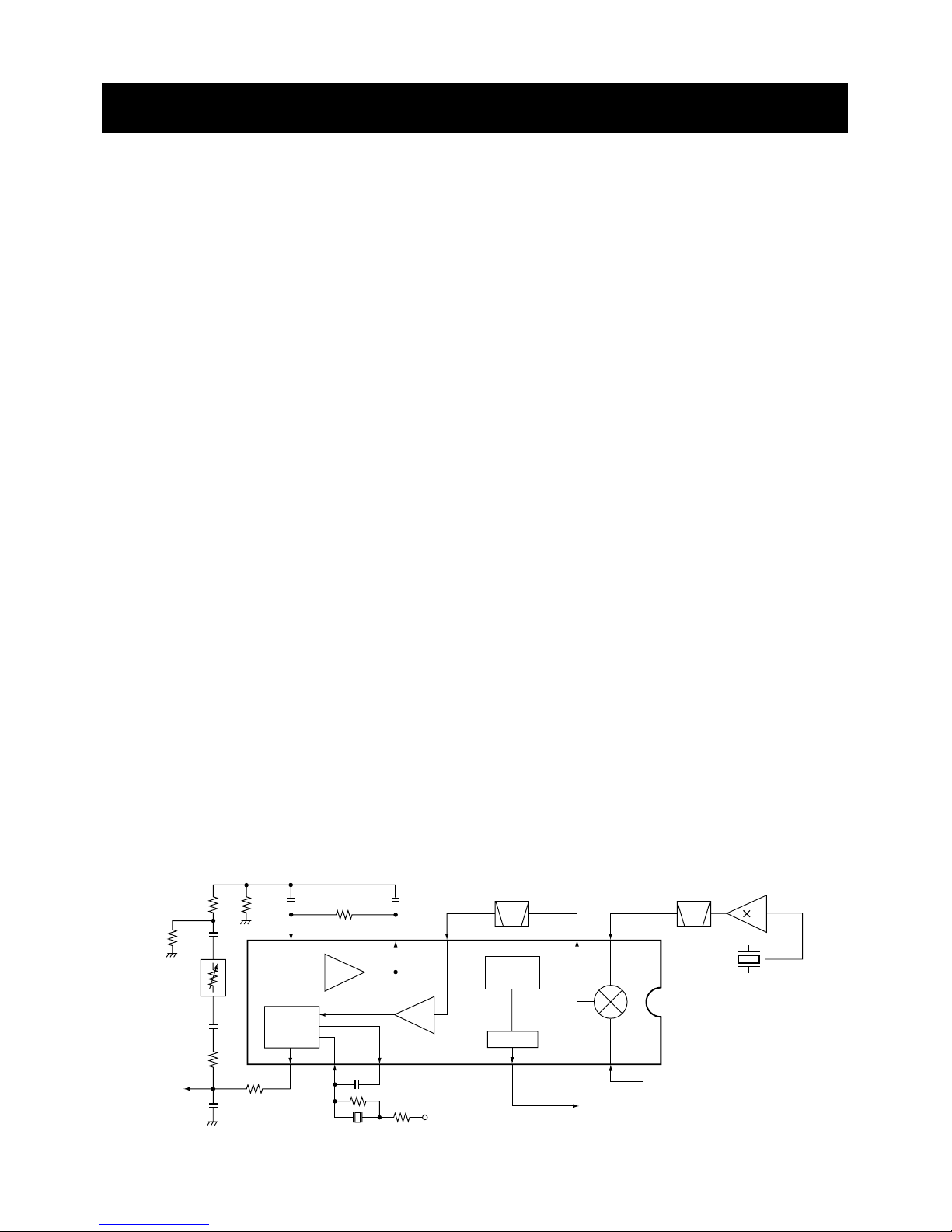
The AF amplifier circuit amplifies the demodulated AF sig-
nals to drive a speaker.
The AF signals from the FM IF IC (IC1, pin 9) are amplified
at the AF amplifier section of the compander IC (IC14, pins
5, 4) and are then applied to the high-pass filter circuit
(IC21b).
The high-pass filter characteristics are controlled by the
FSW signal from the LCD driver IC (FRONT unit; IC1, pin 6).
When FSW signal is high, the cut-off frequency is shifted
higher to remove CTCSS or DTCS signals.
The filtered AF signals from the high-pass filter (IC21b,
pin 7) are applied to the de-emphasis section of compander
IC (IC14, pin 3) with frequency characteristics of –6
dB/octave, and are then passed through the low-pass filter,
high-pass filter, expander sections of compander IC (IC14).
The output signal from IC14 (pin 38) is applied to the elec-
tronic volume controller (IC6, pin 1).
The output AF signals from the electronic volume controller
(IC6, pin 2) are applied to the AF amplifier (IC18) and AF
power amplifier (IC8) to drive the speaker.
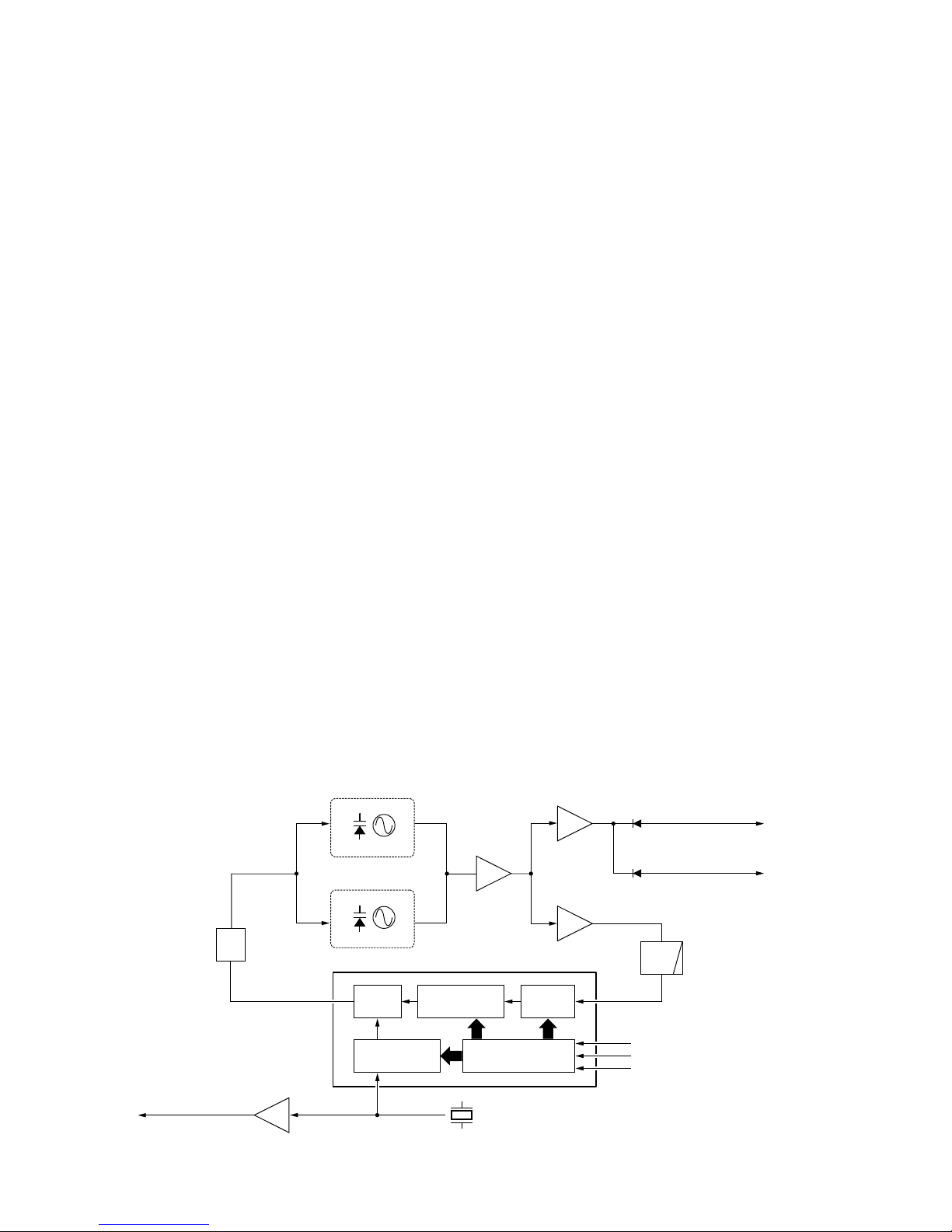
4-1-6 RECEIVER MUTE CIRCUITS (MAIN unit)
• NOISE SQUELCH
The noise squelch circuit cuts out AF signals when no RF
signals are received. By detecting noise components in the
AF signals, the squelch circuit switches the AF mute switch.
Some noise components in the AF signals from the FM IF IC
(IC1, pin 9) are passed through the level controller (IC6, pins
24, 23). The level controlled signals are applied to the active
filter section in the FM IF IC (IC1, pin 8). Noise components
about 10 kHz are amplified and output from pin 7.
The filtered signals are converted into the pulse-type signals
at the noise detector section and output from pin 13 (NOIS).
The NOIS signal from the FM IF IC is applied to the CPU
(IC20, pin 37). The CPU then analyzes the noise condition
and controls the AF mute signal via “AFON”line (IC20, pin
18) to the AF regulator (Q39, Q40, D31).
•CTCSS AND DTCS
The tone squelch circuit detects AF signals and opens the
squelch only when receiving a signal containing a matching
subaudible tone (CTCSS or DTCS). When tone squelch is in
use, and a signal with a mismatched or no subaudible tone
is received, the tone squelch circuit mutes the AF signals
even when noise squelch is open.
A portion of the AF signals from the FM IF IC (IC1, pin 9)
passes through the low-pass filter (IC5) to remove AF
(voice) signals and is applied to the CTCSS or DTCS
decoder inside the CPU (IC20, pin 46) via the “CDEC”line
to control the AF mute switch.
4-2 TRANSMITTER CIRCUIT
4-2-1 MICROPHONE AMPLIFIER CIRCUIT
(MAIN unit)
The microphone amplifier circuit amplifies audio signals
within +6 dB/octave pre-emphasis characteristics from the
microphone to a level needed for the modulation circuit.
The AF signals (MIC) from the FRONT unit via J2 (pin 1) are
passed through the level controller (IC6, pins 9, 10) to the
microphone amplifier circuit.
The AF signals from the level controller (IC6) are applied to
the microphone amplifier section of compander IC (IC14, pin
12). The amplified signals are passed through the compres-
sor, low-pass filter and high-pass filter sections of IC14.
The filtered AF signals are amplified at the buffer amplifier
(Q21) and pre-emphasized with +6dB/octave at the pre-
emphasis circuit (R122, C187), and are then applied to the
IDC amplifier section of IC14 (pin 8).
The amplified AF signals are passed through the limitter
amplifier, low-pass filter and smoothing filter sections of
IC14 after being passed through the AF mute switch inside
of IC14.
The output signals from pin 6 are passed through the ana-
log switch (IC15), splatter filter (IC21d) and applied to the
level controller (IC6, pins 21, 22). The deviation level con-
trolled signals are then applied to modulation circuit as the
“MOD”signal.
The narrow/wide switch (Q22) is connected to the input of
the splatter filter (IC21d) and switched by the “NWC”signal
coming from the CPU (IC20, pin 19). When “NWC”is at a
high level, the narrow/wide switch (Q22) shifts the filter cut-
off frequency for narrow deviation selection.
4-2-2 MODULATION CIRCUIT
The modulation circuit modulates the VCO oscillating signal
(RF signal) using the microphone audio signals.
The AF signals from the level controller (IC6, pin 22) change
the reactance of varactor diode (D18) to modulate the oscil-
lated signal at the TX VCO circuit (Q14, D17). The modulat-
ed VCO signal is amplified at the buffer amplifiers (Q11,
Q10) and is then applied to the drive amplifier circuit via the
T/R switch (D14).
The CTCSS/DTCS signals from the CPU (IC20, pins 89–91)
are passed through the low-pass filter (Q37), level controller
(IC6, pins 12, 11) and mixer (IC21a), and are then applied to
the VCO circuit via the splatter filter (IC21d).
4-2-3 DRIVE AMPLIFIER CIRCUIT (MAIN unit)
The drive amplifier circuit amplifies the VCO oscillating sig-
nal to the level needed at the power amplifier.
The RF signal from the buffer amplifier (Q10) passes
through the T/R switch (D14) and is amplified at the YGR
(Q9) and pre-drive (Q8) amplifiers. The amplified signal is
applied to the power amplifier circuit.

4 - 3
4-2-4 POWER AMPLIFIER CIRCUIT (MAIN unit)
The power amplifier circuit amplifies the driver signal to an
output power level.
The RF signal from the pre-drive amplifier (Q8) is applied to
the power module (IC3) to obtain 25 W for IC-F610/F620, or
45 W for IC-F621 of RF power.
The amplified signal is passed through the antenna switch-
ing circuit (D2), low-pass filter and APC detector, and is then
applied to the antenna connector.
Control voltage for the power amplifier (IC3, pin 3) comes
from the APC amplifier (IC2) to stabilize the output power.
The transmit mute switch (D32) controls the APC amplifier
when transmit mute is necessary.
4-2-5 APC CIRCUIT (MAIN unit)
The APC circuit protects the power amplifier from a mis-
matched output load and stabilizes the output power.
The APC detector circuit detects forward signals and reflec-
tion signals at D11 and D1 respectively. The combined volt-
age is at minimum level when the antenna impedance is
matched at 50 Ω, and is increased when it is mismatched.
The detected voltage is applied to the APC amplifier (IC2,
pin 3), and the power setting “T4”signal from the D/A con-
verter (IC7, pin 4), controlled by the CPU (IC20), is applied
to the other input for reference. When antenna impedance is
mismatched, the detected voltage exceeds the power set-
ting voltage. Then the output voltage of the APC amplifier
(IC2, pin 4) controls the input current of the power module
(IC3) to reduce the output power.
4-3 PLL CIRCUITS
4-3-1 PLL CIRCUIT
A PLL circuit provides stable oscillation of the transmit fre-
quency and receive 1st LO frequency. The PLL output com-
pares the phase of the divided VCO frequency to the refer-
ence frequency. The PLL output frequency is controlled by
the divided ratio (N-data) of a programable divider.
The PLL circuit contains the TX/RX VCO circuit (Q14, Q13).
The oscillated signal is amplified at the buffer amplifiers
(Q11, Q12) and then applied to the PLL IC (IC4, pin 5) via
the low-pass filter (L32, C298, C299).
The PLL IC contains a prescaler, programable counter, pro-
gramable divider and phase detector, etc. The entered sig-
nal is divided at the prescaler and programable counter sec-
tion by the N-data ratio from the CPU. The reference signal
is generated at the reference oscillator (X2) and is also
applied to the PLL IC. The PLL IC detects the out-of-step
phase using the reference frequency and outputs it from
pin 9. The output signal is passed thorough the loop filter
and is then applied to the VCO circuit as the lock voltage.
If the oscillated signal drifts, its phase changes from that of
the reference frequency, causing a lock voltage change to
compensate for the drift in the oscillated frequency.
4-3-2 VCO CIRCUIT
The VCO circuit contains a separate RX VCO (Q13, D16)
and TX VCO (Q14, D17, D18). The oscillated signal is ampli-
fied at the buffer amplifiers (Q11, Q10) and is then applied to
the T/R switch circuit (D14, D15). Then the receive 1st LO
(Rx) signal is applied to the 1st mixer (Q3) and the transmit
(Tx) signal to the YGR amplifier circuit (Q9).
A portion of the signal from the buffer amplifier (Q11) is fed
back to the PLL IC (IC4, pin 5) via the buffer amplifier (Q12)
and low-pass filter (L32, C298, C299) as the comparison
signal.
•PLL circuit
Shift register
×3
Prescaler
Phase
detector
Loop
filter
Programable
counter
Programable
divider
X2
15.3 MHz
45.9 MHz signal
to the FM IF IC 16
Q13, D16
RX VCO
TX VCO
Buffer
Buffer
Buffer
Q10
Q12
Q11
Q34
19
18
17
PLST
IC4 (PLL IC)
SO
SCK
to transmitter circuit
to 1st mixer circuit
D15
D14
85
Q14, D17, D18
LPF

4-4 POWER SUPPLY CIRCUITS
4-4-1 VOLTAGE LINES (MAIN unit)
4-5 PORT ALLOCATIONS
4-5-1 OUTPUT EXPANDER (FRONT unit; IC1)
4-5-2 OUTPUT EXPANDER (MAIN unit; IC7)
4-5-3 CPU (MAIN unit; IC20)
Description
The voltage from a DC power supply.
The same voltage as the HV line which is con-
trolled by the power switching circuit (Q23, Q24).
When the [POWER] switch is pushed, the CPU
outputs the “PWON”control signal to the power
switching circuit to turn the circuit ON.
Common 5 V for the CPU converted from the HV
line by the CPU5V regulator circuit (IC10). The
circuit outputs the voltage regardless of the
power ON/OFF condition.
Common 8 V converted from the VCC line by the
8V regulator circuit (IC9).
Common 5 V converted from the VCC line by the
5V regulator circuit (Q27, Q28).
Receive 8 V controlled by the R8 regulator circuit
(Q26, Q30, D24) using the “TXC”signal from the
CPU (IC20, pin 16).
Transmit 8 V controlled by the T8 regulator circuit
(Q25, Q29, D23) using the “TMUT”signal from
the CPU (IC20, pin 17).
Line
HV
VCC
CPU5V
8V
5V
R8V
T8V
I/O port for data signals from/to the D/A
converter (IC7).
Outputs strobe signals for the level
controller (or D/A converter) (IC6).
Output ports for LCD control signals to
the LCD driver (FRONT unit; IC1)
Outputs clock signal for the LCD driver
(FRONT unit; IC1)
Outputs data signals for the LCD driver
(FRONT unit; IC1)
Outputs strobe signals for the PLL IC
(IC4).
Outputs R8 regulator circuit (Q26, Q30,
D24) control signal.
Outputs T8 regulator circuit (Q25, Q29,
D23) control signal.
Outputs control signal for the AF regu-
lator circuit (Q39, Q40, D31).
High : While AF amplifier (IC8) is acti-
vated.
Outputs IF bandwidth control signal.
High : While IF bandwidth is narrow.
Input port for the data signals from the
DTMF decoder (IC19).
Outputs clock signal to the DTMF
decoder (IC19).
Outputs data signals to the PLL IC
(IC4), level controller (or D/A converter)
(IC6), compander IC (IC14) and option-
al board (connect to J1).
Input port for the clock signal from the
optional board via J1.
Outputs clock signal to the PLL IC
(IC4), level controller (or D/A converter)
(IC6), D/A converter (IC7), compander
IC (IC14) and optional board (connect
to J1).
Outputs chip select signal for the
optional board via J1.
Input ports for the key matrix.
Input port for the PTT switch from the
optional board via J1.
Low : External PTT switch is ON.
Input port for the microphone hanger
detection signal.
Low : Microphone on hook
Outputs BUSY detection signal for the
optional board via J1.
Input port for AF mute signal from the
optional board via J1.
1
2
8,
9
10
11
13
16
17
18
19
20
21
22
23
24
25
26–28
29
30
31
32
DSDA
DAST
LINH,
LCS
LCK
LSO
PLST
TXC
TMUT
AFON
NWC
DDSD
DDAC
SO
SI
SCK
CCS
KR2–
KR0
PTTO
HANG
BUSY
RMUT
Pin Port Description
number name
4 - 4
Output tunable band pass filter control
signals.
Output port for
tunable band pass filter control signal
while receiving.
output power control signal while
transmitting.
1–3
4
T1–T3
T4
Pin Port Description
number name
Output ports for key matrix.
Outputs LCD backlight control signal.
Low : While LCD backlight is dim.
Outputs LCD backlight control signal.
Low : While LCD backlight is OFF.
Outputs high-pass filter’s characteris-
tics select signal.
Outputs external device control signal.
High :
When matched 2/5-tone signals
are received.
Output ports for LCD control signal.
1–3
4
5
6
7
12–55
KS0–KS2
DIM1
DIM2
FSW
HORN
SEG1–SEG40,
COM1–COM4
Pin Port Description
number name

4 - 5
CPU (IC20)—continued CPU (IC20)—continued
Input port for MIC mute signal from the
optional board via J1.
I/O ports for the optional board control
signals.
NOIS signal input port from the FM IF
IC (MAIN unit; IC1) for noise squelch
operation.
Input for the POWER switch.
Low :
While POWER switch is pushed.
Input port for DTMF detection signal
from the DTMF decoder (IC19).
Remote power control signal input port
from the external connector (J8).
Outputs control signal for the power
switching circuit (Q24, Q23) via D28.
Outputs single tone signal.
Outputs beep audio signals.
Single tone signal input port for decod-
ing from the LPF (IC21c).
CTCSS/DTCS signals input port for
decoding from the LPF (IC5).
Input port for the PLL unlock signal
from the PLL IC (IC4).
Input port for the overvoltage detection
from the connected power supply.
Input port for the PLL lock voltage.
Input port for receiving signal strength
level detection.
Input port for the transceiver’s internal
temperature.
Input port for the AF volume control
(FRONT unit; R12).
High : [VOL] is maximum clockwise.
Input port for the PTT switch from the
external connector (J6).
Low : External PTT switch is ON.
Input port for the reset signal.
Output port for the cloning signal.
Input port for the cloning signal.
Outputs CPU clock shift signal.
Outputs cut-off frequency control signal
to the low-pass filter (IC5) for
CTCSS/DTCS switching.
Input port for the connected modem
unit via external connector (J9).
Output port for the connected modem
unit via external connector (J9).
33
34–36
37
38
39
40
41
43
44
45
46
47
48
49
50
51
52
55
59
68
69
70
71
74
75
MMUT
OPT1–
OPT3
NOIS
POSW
DDST
IGSW
PWON
SENC
BEEP
SDEC
CDEC
ULCK
BATV
LVIN
RSSI
TEMP
AFVI
EPTT
RES
CLO
CLI
CSFT
DUSE
XCTS
XRTS
Pin Port Description
number name
Input port for serial data signals from
the connected MAP27 unit via external
connector (J9).
Outputs serial data signals for the con-
nected MAP27 unit via external con-
nector (J9).
Output serial data signals (data format
is in accordance with NMEA0183) for
the connected unit via external connec-
tor (J8).
Input port for serial data signals (data
format is in accordance with
NMEA0183) from the connected unit
via external connector (J8).
Input port for interruption signal from
the optional board via J1
Input port for the LCD backlight control
signal from the external connector (J6).
Output ports for the CTCSS/ DTCS sig-
nals.
Outputs reset signal for the compander
IC (IC14).
Output control signals for the compan-
der IC (IC14).
Outputs strobe signals to the compan-
der IC (IC14).
Outputs control signal for the MSK
PM/FM switching circuit (IC15).
I/O port for the data signals from the
EEPROM (IC23).
Outputs clock signal for the EEPROM
(IC23).
Outputs MIC audio select signal for the
analog switch (IC25).
Low : While “Public-address”function
is ON.
76
77
79
80
81
88
89–91
92
94,
95
96
97
98
99
100
XTXD
XRXD
NTXD
NRXD
CIRQ
DIM
CENC2–
CENC0
AFCL
AMSK,
ADIN
APST
PMFM
ESDA
ESCL
PA
Pin Port Description
number name

■REQUIRED TEST EQUIPMENT
Note: [MPT] versions must use ‘CS-F600’instead of ‘CS-F500’.
5-1 PREPARATION
When you adjust the contents on pages 5-4 and 5-5, SOFT-
WARE ADJUSTMENT, the optional CS-F500 ADJ ADJUSTMENT
SOFTWARE (Rev. 1.0 or later), *OPC-1122 JIG CABLE (modified
OPC-1122 CLONING CABLE; see illustration below) are required.
■SYSTEM REQUIREMENTS
•IBM PC compatible computer with an RS -232C serial port
(38400 bps or faster)
•Microsoft Windows 95/98 or Windows ME
•Intel Pentium 100 MHz processor or faster
•At least 16 MB RAM and 10 MB of hard disk space
•640×480 pixel display (800×600 pixel display recommended)
■ADJUSTMENT SOFTWARE INSTALLATION
qBoot up Windows.
- Quit all applications when Windows is running.
wInsert the ‘CS-F500’into the appropriate CD-ROM drive.
eSelect ‘Run’from the [Start] menu.
rType the setup program name using the full path name,
then push [Enter] key.
(ex. D:\CSF500ADJ\disk1\Setup.exe)
tFollow the prompts.
yProgram group ‘CS-F500 ADJ’appears in the ‘Programs’
folder of the [Start] menu.
■STARTING SOFTWARE ADJUSTMENT
qConnect IC-F610, F620 or F621 and PC with *OPC-1122
JIG CABLE.
wTurn the transceiver power ON.
eBoot up Windows, and click the program group ‘CS-F500
ADJ’in the ‘Programs’folder of the [Start] menu, then
CS-F500 ADJ’s window appears.
rClick ‘Connect’on the CS-F500’s window, then appears
IC-F610, F620 or F621’s up-to-date condition.
tSet or modify adjustment data as desired.
5 - 1
EQUIPMENT
DC power supply
RF power meter
(terminated type)
Frequency counter
FM deviation meter
DC voltmeter
GRADE AND RANGE
Output voltage : 13.2 (13.6) V DC
Current capacity : 20 A or more
Measuring range : 1–75 W
Frequency range : 300–600 MHz
Impedance : 50 Ω
SWR : Less than 1.2 : 1
Frequency range : 0.1–600 MHz
Frequency accuracy : ±1 ppm or better
Sensitivity : 100 mV or better
Frequency range : DC–600 MHz
Measuring range : 0 to ±10 kHz
Input impedance : 50 kΩ/V DC or better
EQUIPMENT
Audio generator
Standard signal
generator (SSG)
Oscilloscope
AC millivoltmeter
External speaker
Attenuator
GRADE AND RANGE
Frequency range : 300–3000 Hz
Measuring range : 1–500 mV
Frequency range : 0.1–600 MHz
Output level : 0.1 µV–32 mV
(–127 to –17 dBm)
Frequency range : DC–20 MHz
Measuring range : 0.01–20 V
Measuring range : 10 mV–10 V
Input impedance : 4 Ω
Capacity : 7 W or more
Power attenuation : 50 or 60 dB
Capacity : 100 W or more
SECTION 5 ADJUSTMENT PROCEDURES
+Audio generator
300 Hz to 3 kHz
AC
millivoltmeter
MICE
MIC
PTT
PTT switch
PTTE
Add a jumper wire here
•*OPC-1122 (JIG CABLE)
Electrolytic
capacitor
47 µF
OPC-1122
(Cloning cable)
IBM is a registered trademark of International Bussiness
Machines Corporation in the U.S.A. and other countries.
Microsoft and Windows are registered trademarks of
Microsoft Corporation in the U.S.A. and other countries.
Screen shots produced with permission from Microsoft
Corporation. All other products or brands are registered
trademarks or trademarks of their respective holders.

5 - 2
FM deviation meter
(DC measurable)
Attenuator
50 dB or 60 dB
to the MIC
connector
to the antenna connector
to DC cable
to an RS-232C port
DB9 female plug
Personal
computer
Standard signal generator
–127 to –17 dBm
(0.1 µV to 32 mV)
CAUTION:
DO NOT transmit while
SSG is connected to
the antenna connector.
RF power meter
50 Ω/ 1–75 W
DC power supply
13.2 (13.6) V / 20 A
Frequency
counter
RS-232C cable
(straight)
*OPC-1122
(JIG CABLE) AC millivoltmeter
Audio generator
•Connections
CS-F500 ADJ Rev.1.0
File
COM 1: OPEN
Option
Connect Reload (F5) Disp para
[A / D]
VIN : 156 : 9Ch : 12.24 V
TEMPS : 187 : BBh : 30.81 'C
LVIN : 57 : 32h : 0.98 V
SD : 36 : 24h : 0.71 V
Power (Hi) : 181 [ # # # # # # # # # # # # # # ––––––]
Power (L2) : 120 [ # # # # # # # # # –––––––––––]
Power (L1) : 69 [ # # # # # –––––––––––––––]
Ballance : 54 [ # # # # ––––––––––––––––]
MOD W : 157 [ # # # # # # # # # # # # ––––––––]
MOD N : 83 [ # # # # # # # –––––––––––––]
CTCS/DTCS : 67 [ # # # # # –––––––––––––––]
SQL : 0 [ ––––––––––––––––––––]
BPF ALL : [Enter] to sweep
BPF T1 : 0 [ # # # # # # # # # –––––––––––] [Enter] to sweep
BPF T2 : 0 [ # # # # # # # # # –––––––––––] [Enter] to sweep
BPF T3 : 0 [ # # # # # # # # # –––––––––––] [Enter] to sweep
BPF T4 : 0 [ # # # # # # # # # –––––––––––] [Enter] to sweep
TXF : [Enter] to start
S-METER : [Enter] to start
[D / A]
BPF T1 : 50 : 32h : 0.98 V
BPF T2 : 50 : 32h : 0.98 V
BPF T3 : 50 : 32h : 0.98 V
T4/POW : 50 : 32h : 0.98 V
REF : 45 : 2Dh : 0.88 V
MOD BAL : 54 : 36h : 21.18 %
Dev : 157 : 9Dh : 3.08 V
CTCSS : 66 : 42h : 1.29 V
SQL Lev : 0 : 00h : 0.00 %
CH No. : 01 RX Freq = 440.050, TX Freq = <–RF Power: High Mode: Wide
: Transceiver's connection state
: Reload adjustment data
:
Receive sensitivity measurement
: Connected DC voltage
NOTE:
•Screen display exampe
1
5
4
6
10
11
12
15
9
14
16
1
2
3
4
9
10
: PLL lock voltage
:
Operating channel select
: RF output power
: Modulation balance
5
6
7
8
11
12
: FM deviation
:
CTCSS/DTCS deviation
: Squelch level
: Receive sensitivity
(automatically)
13 :
Receive sensitivity (manually)
: Reference frequency
: S-meter
: Adjustment items
14
15
16
The above values for settings are example only.
Each transceiver has its own specific values for each setting.
3
2
8
7
13

LV
PLL lock voltage
check point
C134
PLL lock voltage
adjustment for TX
C133
PLL lock voltage
adjustment for RX
DC power supply
13.2 (13.6) V / 20 A
5 - 3
5-2 PLL ADJUSTMENT
PLL LOCK
VOLTAGE
1
2
3
4
•Operating freq. : 400.000 MHz [L]
440.000 MHz [M]
480.000 MHz [H]
•Receiving
•Output power : Low1
•Transmitting
•Operating freq. : 430.000 MHz [L]
490.000 MHz [M]
520.000 MHz [H]
•Receiving
•Output power : Low1
•Transmitting
MAIN Connect a digital multi-
meter or an oscillo-
scope to the check
point, “LV”.
1.0 V
1.1 V
3.0–4.2 V [L]
3.3–4.5 V [M]
3.3–4.5 V [H]
MAIN C133
C134
Verify
ADJUSTMENT ADJUSTMENT CONDITIONS
UNIT LOCATION
VALUE
UNIT ADJUST
MEASUREMENT ADJUSTMENT

5 - 4
5-3 SOFTWARE ADJUSTMENT
Select an operation using [↑] / [↓] keys, then set specified value using [←] / [→] keys on the connected computer keyboard.
1
1
2
3
1
1
2
•Operating freq. : 430.000 MHz [L]
490.000 MHz [M]
520.000 MHz [H]
•Output power : Low1
•Connect the RF power meter or 50 Ω
dummy load to the antenna connector.
•Transmitting
•Operating freq. : 400.000 MHz [L]
440.000 MHz [M]
480.000 MHz [H]
•Output power : High
•Transmitting
•Output power : Low2
•Transmitting
•Output power : Low1
•Transmitting
•Operating freq. : 415.000 MHz [L]
465.000 MHz [M]
500.000 MHz [H]
•Output power : Low1
•Push [P0] key while transmitting
•Operating freq. : 415.000 MHz [L]
465.000 MHz [M]
500.000 MHz [H]
•Output power : Low1
•IF bandwidth : Wide
•Connect an audio generator to the [MIC]
jack through the JIG cable and set as:
1.0 kHz/40 mVrms
•Set an FM deviation meter as:
HPF : OFF
LPF : 20 kHz
De-emphasis: OFF
Detector : (P–P)/2
•Transmitting
•IF bandwidth : Narrow
•Transmitting
•Operating freq. : 415.000 MHz [L]
465.000 MHz [M]
500.000 MHz [H]
•Output power : Low1
•IF bandwidth : Wide
•CTCSS : 88.5 Hz
•DTCS code : 007
•Set the FM deviation meter as:
HPF : OFF
LPF : 20 kHz
De-emphasis: OFF
Detector : (P–P)/2
•No audio applied to the [MIC] connector.
•Transmitting
REFERENCE
FREQUENCY
[TXF]
OUTPUT
POWER
[Power (Hi)]
[Power (L2)]
[Power (L1)]
MODULATION
BALLANCE
[Ballance]
FM
DEVIATION
[MOD W]
[MOD N]
CTCSS/DTCS
DEVIATON
[CTCS/DTCS]
Rear
panel
Rear
panel
Rear
panel
Rear
panel
Rear
panel
Loosely couple a frequnecy
counter to the antenna connec-
tor.
Connect an RF power meter to
the antenna connector.
Connect an FM deviation meter
with an oscilloscope to the
antenna connector through an
attenuator.
Connect an FM deviation meter
to the antenna connector
through the attenuator.
Connect an FM deviation meter
to the antenna connector
through the attenuator.
430.0000 MHz [L]
490.0000 MHz [M]
520.0000 MHz [H]
25.0 W [25W]
45.0 W [45W]
10.0 W [25W]
25.0 W [45W]
2.5 W [25W]
4.5 W [45W]
±4.1 kHz [N/W]
±3.3 kHz [N/M]
±2.1 kHz
±0.70 kHz [N/W]
±0.56 kHz [N/M]
ADJUSTMENT ADJUSTMENT CONDITION MEASUREMENT VALUE
UNIT LOCATION
Set to square wave
form

*The output level of the standard signal generator (SSG) is indicated as the SSG’s open circuit.
5 - 5
SOFTWARE ADJUSTMENT –continued
Select an operation using [↑] / [↓] keys, then set specified value using [←] / [→] keys on the connected computer keyboard.
Minimum distortion
level
Push [ENTER] key
on the connected
computer keyboard
to set “S3 level”.
Push [ENTER] key
on the connected
computer keyboard
to set “S1 level”.
Set “SQL level”to
close squelch.
Then set “SQL level”
at the point where
the audio signals
just appears.
1
1
2
1
•Operating freq. : 400.000 MHz [L]
440.000 MHz [M]
480.000 MHz [H]
•IF bandwidth : Wide
•Connect a standard signal generator to
the antenna connector and set as:
Frequency : 400.000 MHz [L]
440.000 MHz [M]
480.000 MHz [H]
Level : 10 µV* (–87 dBm)
Modulation : 1 kHz
Deviation : ±3.5 kHz [N/W]
±2.8 kHz [N/M]
•Receiving
•Operating freq. : 400.000 MHz [L]
440.000 MHz [M]
480.000 MHz [H]
•IF bandwidth : Wide
•Connect an SSG to the antenna con-
nector and set as:
Frequency : 400.000 MHz [L]
440.000 MHz [M]
480.000 MHz [H]
Level : 14 µV* (–84 dBm)
Modulation : 1 kHz
Deviation : ±3.5 kHz [N/W]
±2.8 kHz [N/M]
•Receiving
•Set an SSG as :
Level : 0.45 µV* (–114 dBm)
Modulation : 1 kHz
Deviation : ±3.5 kHz [N/W]
±2.8 kHz [N/M]
•Receiving
•Operating freq. : 415.000 MHz [L]
465.000 MHz [M]
500.000 MHz [H]
•IF bandwidth : Narrow
•Connect an SSG to the antenna con-
nector and set as:
Frequency : 415.000 MHz [L]
465.000 MHz [M]
500.000 MHz [H]
Level : 0.2 µV* (–121 dBm)
Modulation : 1 kHz
Deviation : ±1.75 kHz
•Receiving
RX
SENSITIVITY
[BPF T1] –
[BPF T4]
S-METER
[S-METER]
SQUELCH
LEVEL
[SQL]
MAIN
Rear
panel
Connect a SINAD meter with a
4Ωload to the external [SP]
jack.
Connect a SINAD meter with a
4Ωload to the external [SP]
jack.
ADJUSTMENT ADJUSTMENT CONDITION MEASUREMENT VALUE
UNIT LOCATION
CONVENIENT:
The BPF T1–BPF T4 can be adjusted automatically.
q-1: Set the cursol to “BPF ALL”on the adjustment program and then push [ENTER] key.
q-2: The connected PC tunes BPF T1–BPF T4 to peak levels.
or
w-1: Set the cursol to one of BPF T1, T2, T3, or T4 as desired.
w-2: Push [ENTER] key to start tuning.
w-3: Repeat w-1 and w-2 to perform additional BPF tuning.

[FRONT UNIT][FRONT UNIT]
IC1 1130010800 S.IC LC75824W
IC2 1130008560 S.IC TC75S51F (TE85L)
Q1 1590000720 S.TRANSISTOR DTA144EUA T106
Q2 1590000430 S.TRANSISTOR DTC144EUA T106
Q3 1590000430 S.TRANSISTOR DTC144EUA T106
Q4 1590000720 S.TRANSISTOR DTA144EUA T106
D1 1790001670 S.DIODE RB706F-40T106
D2 1790001670 S.DIODE RB706F-40T106
D3 1790001670 S.DIODE RB706F-40T106
D4 1790001250 S.DIODE MA2S111-(TX)
D5 1790001250 S.DIODE MA2S111-(TX)
D6 1790001250 S.DIODE MA2S111-(TX)
L1 6200003960 S.COIL MLF1608A 1R0K-T
R1 7030003440 S.RESISTOR ERJ3GEYJ 102 V (1 kΩ)
R2 7030003440 S.RESISTOR ERJ3GEYJ 102 V (1 kΩ)
R3 7030003390 S.RESISTOR ERJ3GEYJ 391 V (390 Ω)
R4 7030003390 S.RESISTOR ERJ3GEYJ 391 V (390 Ω)
R5 7030003520 S.RESISTOR ERJ3GEYJ 472 V (4.7 kΩ)
R6 7030003440 S.RESISTOR ERJ3GEYJ 102 V (1 kΩ)
R7 7030000330 S.RESISTOR MCR10EZHJ 390 Ω(391)
R8 7410000950 S.ARRAY EXB-V8V 102JV
R9 7410000770 S.ARRAY EXB-V4V 102JV (1 kΩ)
R10 7030003680 S.RESISTOR ERJ3GEYJ 104 V (100 kΩ)
R11 7030003680 S.RESISTOR ERJ3GEYJ 104 V (100 kΩ)
R12 7210003020 VARIABLE EVU-F2KFK1 B14 (10KB)
R13 7030003730 S.RESISTOR ERJ3GEYJ 274 V (270 kΩ)
R14 7030003680 S.RESISTOR ERJ3GEYJ 104 V (100 kΩ)
R16 7030003440 S.RESISTOR ERJ3GEYJ 102 V (1 kΩ)
R17 7030003560 S.RESISTOR ERJ3GEYJ 103 V (10 kΩ)
R18 7030003560 S.RESISTOR ERJ3GEYJ 103 V (10 kΩ)
R19 7030003560 S.RESISTOR ERJ3GEYJ 103 V (10 kΩ)
R20 7030003510 S.RESISTOR ERJ3GEYJ 392 V (3.9 kΩ)
R21 7030003800 S.RESISTOR ERJ3GEYJ 105 V (1 MΩ)
R22 7030003560 S.RESISTOR ERJ3GEYJ 103 V (10 kΩ)
R23 7030003560 S.RESISTOR ERJ3GEYJ 103 V (10 kΩ)
R24 7030003480 S.RESISTOR ERJ3GEYJ 222 V (2.2 kΩ)
R25 7030003640 S.RESISTOR ERJ3GEYJ 473 V (47 kΩ)
C1 4030007090 S.CERAMIC C1608 CH 1H 470J-T
C2 4030007090 S.CERAMIC C1608 CH 1H 470J-T
C3 4030007090 S.CERAMIC C1608 CH 1H 470J-T
C4 4030007090 S.CERAMIC C1608 CH 1H 470J-T
C5 4030007090 S.CERAMIC C1608 CH 1H 470J-T
C6 4030007090 S.CERAMIC C1608 CH 1H 470J-T
C7 4030007090 S.CERAMIC C1608 CH 1H 470J-T
C8 4030007090 S.CERAMIC C1608 CH 1H 470J-T
C9 4030007090 S.CERAMIC C1608 CH 1H 470J-T
C10 4030007090 S.CERAMIC C1608 CH 1H 470J-T
C11 4030007090 S.CERAMIC C1608 CH 1H 470J-T
C12 4030007090 S.CERAMIC C1608 CH 1H 470J-T
C13 4030007090 S.CERAMIC C1608 CH 1H 470J-T
C14 4030007090 S.CERAMIC C1608 CH 1H 470J-T
C15 4030007090 S.CERAMIC C1608 CH 1H 470J-T
C16 4030007090 S.CERAMIC C1608 CH 1H 470J-T
C17 4030007090 S.CERAMIC C1608 CH 1H 470J-T
C18 4030007090 S.CERAMIC C1608 CH 1H 470J-T
C19 4030006860 S.CERAMIC C1608 JB 1H 102K-T
C20 4030006860 S.CERAMIC C1608 JB 1H 102K-T
C21 4030007090 S.CERAMIC C1608 CH 1H 470J-T
C22 4030007090 S.CERAMIC C1608 CH 1H 470J-T
C23 4030007090 S.CERAMIC C1608 CH 1H 470J-T
C24 4030007090 S.CERAMIC C1608 CH 1H 470J-T
C25 4030007090 S.CERAMIC C1608 CH 1H 470J-T
C26 4030007090 S.CERAMIC C1608 CH 1H 470J-T
C27 4030007090 S.CERAMIC C1608 CH 1H 470J-T
C28 4030007090 S.CERAMIC C1608 CH 1H 470J-T
C29 4030007090 S.CERAMIC C1608 CH 1H 470J-T
S.=Surface mount
C30 4030011600 S.CERAMIC C1608 JB 1E 104K-T
C31 4030011600 S.CERAMIC C1608 JB 1E 104K-T
C32 4030011600 S.CERAMIC C1608 JB 1E 104K-T
C33 4030007130 S.CERAMIC C1608 CH 1H 101J-T
C34 4030007090 S.CERAMIC C1608 CH 1H 470J-T
C35 4030007090 S.CERAMIC C1608 CH 1H 470J-T
C37 4550000550 S.TANTALUM TESVA 1V 224M1-8L
C39 4030006900 S.CERAMIC C1608 JB 1H 103K-T
C40 4550005980 S.TANTALUM TEMSVA 1A 475M-8L
C41 4030006860 S.CERAMIC C1608 JB 1H 102K-T
J1 6450002210 CONNECTOR 3017-8821
J2 6510023090 S.CONNECTOR 20FLT-SM1-TB
DS1 5040002310 S.LED SML-311YTT86
DS2 5040002310 S.LED SML-311YTT86
DS3 5040002310 S.LED SML-311YTT86
DS4 5040002310 S.LED SML-311YTT86
DS5 5040002310 S.LED SML-311YTT86
DS6 5040002310 S.LED SML-311YTT86
DS7 5040002310 S.LED SML-311YTT86
DS8 5040002310 S.LED SML-311YTT86
DS9 5040002310 S.LED SML-311YTT86
DS10 5040002310 S.LED SML-311YTT86
DS11 5040002310 S.LED SML-311YTT86
DS12 5030002230 LCD L1-0483TAT
W1 8900010950 CABLE OPC-1126 (P=0.5 N=20 L=90)
EP1 0910054932 PCB B 5809B
EP2 8930057820 LCD CONTACT SRCN-2526-SP-N-W
6 - 1
SECTION 6 PARTS LIST
REF ORDER DESCRIPTION
NO. NO.
REF ORDER DESCRIPTION
NO. NO.

S.=Surface mount
[MAIN UNIT][MAIN UNIT]
IC1 1110003490 S.IC TA31136FN (D, EL)
IC2 1130008560 S.IC TC75S51F (TE85L)
IC3 1150002090 IC RA30H4047M-01 [L]
1150002030 IC RA30H4452M [M]-25W, [H]
1150002060 IC RA45H4452M [M]-45W
IC4 1130010810 S.IC SA7026DH-T
IC5 1110005330 S.IC NJM12904V-TE1
IC6 1190001350 S.IC M62364FP 600D
IC7 1190001340 S.IC M62334FP 600C
IC8 1110003090 IC LA4425A
IC9 1180001250 S.IC TA7808F (TE16L)
IC10 1180000970 S.IC AN78L05M-(E1)
IC11 1130008560 S.IC TC75S51F (TE85L)
IC14 1130009330 S.IC TC35453F (BR, DRY)
IC15 1130006220 S.IC TC4W53FU (TE12L)
IC18 1110002750 S.IC TA75S01F (TE85R)
IC19 1130009700 S.IC LC73872M-TRM
IC20 1140010190 S.IC HD64F2268TF (EMPTY)
IC21 1110005340 S.IC NJM12902V-TE1
IC22 1130004200 S.IC TC4S66F (TE85R)
IC23 1140009240 S.IC HN58X24128FPI
IC24 1130009110 S.IC S-80942ANMP-DD6-T2
IC25 1130004200 S.IC TC4S66F (TE85R)
Q1 1560000840 S.FET 2SK1829 (TE85R)
Q2 1580000730 S.FET 3SK293 (TE85L)
Q3 1580000660 S.FET 3SK272-(TX)
Q4 1530002600 S.TRANSISTOR 2SC4215-O (TE85R)
Q5 1530002850 S.TRANSISTOR 2SC4116-BL (TE85R)
Q6 1590000720 S.TRANSISTOR DTA144EUA T106
Q8 1530000372 S.TRANSISTOR 2SC3356 R24-T1B
Q9 1530003310 S.TRANSISTOR 2SC5107-O (TE85R)
Q10 1530003310 S.TRANSISTOR 2SC5107-O (TE85R)
Q11 1530003310 S.TRANSISTOR 2SC5107-O (TE85R)
Q12 1530003310 S.TRANSISTOR 2SC5107-O (TE85R)
Q13 1530002920 S.TRANSISTOR 2SC4226-T1 R25
Q14 1530002920 S.TRANSISTOR 2SC4226-T1 R25
Q15 1590001400 S.TRANSISTOR XP1214 (TX)
Q16 1590000430 S.TRANSISTOR DTC144EUA T106
Q17 1530002850 S.TRANSISTOR 2SC4116-BL (TE85R)
Q18 1560000540 S.FET 2SK880-Y (TE85R)
Q19 1530002600 S.TRANSISTOR 2SC4215-O (TE85R)
Q20 1530003090 S.TRANSISTOR 2SC4213-B (TE85R)
Q21 1530002850 S.TRANSISTOR 2SC4116-BL (TE85R)
Q22 1590000430 S.TRANSISTOR DTC144EUA T106
Q23 1550000020 S.FET 2SJ377 (TE16R)
Q24 1590000430 S.TRANSISTOR DTC144EUA T106
Q25 1540000550 S.TRANSISTOR 2SD1664 T100Q
Q26 1540000550 S.TRANSISTOR 2SD1664 T100Q
Q27 1520000460 S.TRANSISTOR 2SB1132 T100 R
Q28 1590001190 S.TRANSISTOR XP6501-(TX) .AB
Q29 1590000430 S.TRANSISTOR DTC144EUA T106
Q30 1590000430 S.TRANSISTOR DTC144EUA T106
Q31 1590001450 S.FET 2SJ144-GR (TE85R)
Q32 1590000430 S.TRANSISTOR DTC144EUA T106
Q33 1590000430 S.TRANSISTOR DTC144EUA T106
Q34 1530002850 S.TRANSISTOR 2SC4116-BL (TE85R)
Q35 1590001400 S.TRANSISTOR XP1214 (TX)
Q36 1530002850 S.TRANSISTOR 2SC4116-BL (TE85R)
Q37 1530002850 S.TRANSISTOR 2SC4116-BL (TE85R)
Q38 1590000430 S.TRANSISTOR DTC144EUA T106
Q39 1590000990 S.TRANSISTOR DTC363EK T146
Q40 1590000430 S.TRANSISTOR DTC144EUA T106
Q41 1590000720 S.TRANSISTOR DTA144EUA T106
Q42 1590000430 S.TRANSISTOR DTC144EUA T106
Q43 1590000430 S.TRANSISTOR DTC144EUA T106
Q44 1590000430 S.TRANSISTOR DTC144EUA T106
Q48 1590000430 S.TRANSISTOR DTC144EUA T106
Q49 1590000430 S.TRANSISTOR DTC144EUA T106
Q50 1590000430 S.TRANSISTOR DTC144EUA T106
Q51 1530002850 S.TRANSISTOR 2SC4116-BL (TE85R) [45W]
D1 1790000660 S.DIODE MA728 (TX)
D2 1750000510 S.DIODE UM9401F [25W]
D3 1710001060 DIODE XB15A407 [45W]
D4 1750000710 S.VARICAP HVC350BTRF
D5 1750000760 S.DIODE MA4PH224
D6 1790000620 S.DIODE MA77 (TX)
D8 1750000710 S.VARICAP HVC350BTRF
D9 1750000710 S.VARICAP HVC350BTRF
D10 1750000710 S.VARICAP HVC350BTRF
D11 1790000660 S.DIODE MA728 (TX)
D14 1790000620 S.DIODE MA77 (TX)
D15 1790000620 S.DIODE MA77 (TX)
D16 1750000710 S.VARICAP HVC350BTRF
D17 1750000710 S.VARICAP HVC350BTRF
D18 1720000570 S.VARICAP MA368 (TX)
D19 1790001250 S.DIODE MA2S111-(TX)
D20 1790001250 S.DIODE MA2S111-(TX)
D21 1750000830 S.VARICAP HVC362TRF
D22 1790000700 DIODE DSA3A1
D23 1750000370 S.DIODE DA221 TL
D24 1750000370 S.DIODE DA221 TL
D25 1790001250 S.DIODE MA2S111-(TX)
D26 1790001250 S.DIODE MA2S111-(TX)
D27 1790000620 S.DIODE MA77 (TX)
D28 1750000520 S.DIODE DAN222TL
D30 1790001250 S.DIODE MA2S111-(TX)
D31 1750000520 S.DIODE DAN222TL
D32 1790001250 S.DIODE MA2S111-(TX)
D33 1790001250 S.DIODE MA2S111-(TX)
D34 1790001250 S.DIODE MA2S111-(TX)
D35 1750000520 S.DIODE DAN222TL
D36 1750000520 S.DIODE DAN222TL
D37 1750000520 S.DIODE DAN222TL
FI1 2010002450 S.XTAL FL-313 (46.35 MHz) [USA], [GEN]
2030000150 S.MONOLITH FL-335 (46.350 MHz) [EUR]
FI2 2020001840 CERAMIC ALFYM450F=K
FI3 2040001440 S.LC NFE31PT152Z1E9L
FI4 2040001440 S.LC NFE31PT152Z1E9L
FI5 2040001440 S.LC NFE31PT152Z1E9L [45W]
X1 6070000190
S.DISCRIMINATOR
CDBCB450KCAY24-R0
X2 6050011120 S.XTAL CR-671A (15.300 MHz)
X3 6050009910 S.XTAL CR-563 (3.579545 MHz)
X4 6050009520 S.XTAL CR-520 (19.6608 MHz+)
L1 6110001520 COIL LA-232 [25W]
6110002110 COIL LA-382 [45W]
L2 6110001520 COIL LA-232
L3 6110002110 COIL LA-382
L4 6200008330 S.COIL 0.45-1.4-4TL 15N
L5 6170000230 COIL LW-25
L6 6200008330 S.COIL 0.45-1.4-4TL 15N
L7 6200007230 S.COIL LQW2BHN15NJ01L [L]
6200007670 S.COIL LQW2BHN10NJ01L [M], [H]
L8 6200007680 S.COIL LQW2BHN12NJ01L [L]
6200007670 S.COIL LQW2BHN10NJ01L [M], [H]
L9 6200007680 S.COIL LQW2BHN12NJ01L [L]
6200007670 S.COIL LQW2BHN10NJ01L [M], [H]
L11 6200007680 S.COIL LQW2BHN12NJ01L [L]
6200007670 S.COIL LQW2BHN10NJ01L [M], [H]
L12 6200005720 S.COIL ELJRE 33NG-F
L13 6200003350 S.COIL ELJNC R27K-F
L16 6110001520 COIL LA-232 [25W]
6110002110 COIL LA-382 [45W]
L18 6200005690 S.COIL ELJRE 18NG-F [L]
6200005680 S.COIL ELJRE 15NG-F [M], [H]
L19 6200005690 S.COIL ELJRE 18NG-F [L]
6200005680 S.COIL ELJRE 15NG-F [M], [H]
L20 6200005710 S.COIL ELJRE 27NG-F [L]
6200005700 S.COIL ELJRE 22NG-F [M], [H]
L21 6200005710 S.COIL ELJRE 27NG-F [L]
6200005700 S.COIL ELJRE 22NG-F [M], [H]
L22 6200005710 S.COIL ELJRE 27NG-F
L23 6200004950 S.COIL NL 252018T-1R8J
L24 6200004950 S.COIL NL 252018T-1R8J
L25 6200009360 S.COIL 0.45-1.4-3TL 11N
L26 6200009360 S.COIL 0.45-1.4-3TL 11N
L27 6200004950 S.COIL NL 252018T-1R8J
L28 6200004950 S.COIL NL 252018T-1R8J
L29 6200004950 S.COIL NL 252018T-1R8J
L31 6200007740 S.COIL LQW2BHN47NJ01L
L32 6200005690 S.COIL ELJRE 18NG-F [L]
6200005680 S.COIL ELJRE 15NG-F [M], [H]
L33 6200002850 S.COIL NL 252018T-R82J
L35 6200002840 S.COIL NL 252018T-R22J
L36 6200002860 S.COIL NL 252018T-4R7J
6 - 2
REF ORDER DESCRIPTION
NO. NO.
REF ORDER DESCRIPTION
NO. NO.

S.=Surface mount
[MAIN UNIT][MAIN UNIT]
L37 6200006980 S.COIL ELJRE R10G-F
L38 6200005690 S.COIL ELJRE 18NG-F
R1 7030000620 S.RESISTOR MCR10EZHJ 100 kΩ
R2 7030000260 S.RESISTOR MCR10EZHJ 100 Ω(101)
R3 7030000220 S.RESISTOR MCR10EZHJ 47 Ω(470) [25W]
7030000280 S.RESISTOR MCR10EZHJ 150 Ω(151) [45W]
R4 7030003320 S.RESISTOR ERJ3GEYJ 101 V (100 Ω)
R5 7030003320 S.RESISTOR ERJ3GEYJ 101 V (100 Ω)
R6 7030003320 S.RESISTOR ERJ3GEYJ 101 V (100 Ω)
R7 7030003320 S.RESISTOR ERJ3GEYJ 101 V (100 Ω) [25W]
7030003340 S.RESISTOR ERJ3GEYJ 151 V (150 Ω) [45W]
R8 7030001170 S.RESISTOR MCR50JZHJ 220 Ω(221)
R9 7030001170 S.RESISTOR MCR50JZHJ 220 Ω(221)
R10 7030003470 S.RESISTOR ERJ3GEYJ 182 V (1.8 kΩ)
R11 7030003720 S.RESISTOR ERJ3GEYJ 224 V (220 kΩ)
R12 7030003560 S.RESISTOR ERJ3GEYJ 103 V (10 kΩ)
R13 7030003720 S.RESISTOR ERJ3GEYJ 224 V (220 kΩ)
R14 7030003560 S.RESISTOR ERJ3GEYJ 103 V (10 kΩ)
R15 7030003670 S.RESISTOR ERJ3GEYJ 823 V (82 kΩ)
R16 7030003340 S.RESISTOR ERJ3GEYJ 151 V (150 Ω)
R17 7030004050 S.RESISTOR ERJ3GEYJ 1R0 V (1 Ω)
R18 7030003560 S.RESISTOR ERJ3GEYJ 103 V (10 kΩ)
R19 7030003720 S.RESISTOR ERJ3GEYJ 224 V (220 kΩ)
R20 7030003440 S.RESISTOR ERJ3GEYJ 102 V (1 kΩ)
R21 7030003720 S.RESISTOR ERJ3GEYJ 224 V (220 kΩ)
R22 7030003560 S.RESISTOR ERJ3GEYJ 103 V (10 kΩ)
R23 7030003720 S.RESISTOR ERJ3GEYJ 224 V (220 kΩ)
R24 7030003560 S.RESISTOR ERJ3GEYJ 103 V (10 kΩ)
R25 7030003520 S.RESISTOR ERJ3GEYJ 472 V (4.7 kΩ)
R29 7030003330 S.RESISTOR ERJ3GEYJ 121 V (120 Ω)
R30 7030003440 S.RESISTOR ERJ3GEYJ 102 V (1 kΩ)
R31 7030003320 S.RESISTOR ERJ3GEYJ 101 V (100 Ω)
R32 7030003320 S.RESISTOR ERJ3GEYJ 101 V (100 Ω)
R33 7030003340 S.RESISTOR ERJ3GEYJ 151 V (150 Ω)
R34 7030003690 S.RESISTOR ERJ3GEYJ 124 V (120 kΩ)
R35 7030003440 S.RESISTOR ERJ3GEYJ 102 V (1 kΩ)
R36 7030003510 S.RESISTOR ERJ3GEYJ 392 V (3.9 kΩ)
R37 7030003500 S.RESISTOR ERJ3GEYJ 332 V (3.3 kΩ) [N/W]
7030003520 S.RESISTOR ERJ3GEYJ 472 V (4.7 kΩ) [N/M]
R38 7030003680 S.RESISTOR ERJ3GEYJ 104 V (100 kΩ)
R39 7030003280 S.RESISTOR ERJ3GEYJ 470 V (47 Ω)
R40 7030003460 S.RESISTOR ERJ3GEYJ 152 V (1.5 kΩ)
R41 7030003640 S.RESISTOR ERJ3GEYJ 473 V (47 kΩ)
R42 7030003640 S.RESISTOR ERJ3GEYJ 473 V (47 kΩ)
R43 7030003400 S.RESISTOR ERJ3GEYJ 471 V (470 Ω)
R44 7030003640 S.RESISTOR ERJ3GEYJ 473 V (47 kΩ)
R45 7030003620 S.RESISTOR ERJ3GEYJ 333 V (33 kΩ)
R46 7030003460 S.RESISTOR ERJ3GEYJ 152 V (1.5 kΩ)
R47 7030003500 S.RESISTOR ERJ3GEYJ 332 V (3.3 kΩ)
R50 7030003560 S.RESISTOR ERJ3GEYJ 103 V (10 kΩ)
R52 7030003560 S.RESISTOR ERJ3GEYJ 103 V (10 kΩ)
R53 7030003320 S.RESISTOR ERJ3GEYJ 101 V (100 Ω)
R54 7030003560 S.RESISTOR ERJ3GEYJ 103 V (10 kΩ)
R55 7030003480 S.RESISTOR ERJ3GEYJ 222 V (2.2 kΩ) [L]
7030003440 S.RESISTOR ERJ3GEYJ 102 V (1 kΩ) [M], [H]
R56 7030003700 S.RESISTOR ERJ3GEYJ 154 V (150 kΩ)
R57 7030003560 S.RESISTOR ERJ3GEYJ 103 V (10 kΩ)
R58 7030003280 S.RESISTOR ERJ3GEYJ 470 V (47 Ω) [L]
7030003320 S.RESISTOR ERJ3GEYJ 101 V (100 Ω) [M], [H]
R59 7030003560 S.RESISTOR ERJ3GEYJ 103 V (10 kΩ) [25W]
7030003570 S.RESISTOR ERJ3GEYJ 123 V (12 kΩ) [45W]
R61 7030003290 S.RESISTOR ERJ3GEYJ 560 V (56 Ω) [25W]
7030003340 S.RESISTOR ERJ3GEYJ 151 V (150 Ω) [45W]
R62 7030003570 S.RESISTOR ERJ3GEYJ 123 V (12 kΩ) [25W]
7030003600 S.RESISTOR ERJ3GEYJ 223 V (22 kΩ) [45W]
R65 7030003360 S.RESISTOR ERJ3GEYJ 221 V (220 Ω) [25W]
7030003340 S.RESISTOR ERJ3GEYJ 151 V (150 Ω) [45W]
R66 7030003680 S.RESISTOR ERJ3GEYJ 104 V (100 kΩ)
R67 7030003560 S.RESISTOR ERJ3GEYJ 103 V (10 kΩ)
R68 7030003440 S.RESISTOR ERJ3GEYJ 102 V (1 kΩ)
R69 7030003520 S.RESISTOR ERJ3GEYJ 472 V (4.7 kΩ)
R70 7030003320 S.RESISTOR ERJ3GEYJ 101 V (100 Ω)
R71 7030003260 S.RESISTOR ERJ3GEYJ 330 V (33 Ω)
R72 7030003400 S.RESISTOR ERJ3GEYJ 471 V (470 Ω)
R73 7030003360 S.RESISTOR ERJ3GEYJ 221 V (220 Ω)
R74 7030003680 S.RESISTOR ERJ3GEYJ 104 V (100 kΩ)
[L], [M]-45W
7030003660 S.RESISTOR ERJ3GEYJ 683 V (68 kΩ)
[M]-25W, [H]
R75 7030003700 S.RESISTOR ERJ3GEYJ 154 V (150 kΩ)
R76 7030003360 S.RESISTOR ERJ3GEYJ 221 V (220 Ω)
R77 7030003560 S.RESISTOR ERJ3GEYJ 103 V (10 kΩ)
R78 7030003410 S.RESISTOR ERJ3GEYJ 561 V (560 Ω)
R79 7030003500 S.RESISTOR ERJ3GEYJ 332 V (3.3 kΩ)
R80 7030003440 S.RESISTOR ERJ3GEYJ 102 V (1 kΩ)
R81 7030003200 S.RESISTOR ERJ3GEYJ 100 V (10 Ω)
R82 7030004040 S.RESISTOR ERJ3GEYJ 4R7 V (4.7 Ω)
R83 7030003500 S.RESISTOR ERJ3GEYJ 332 V (3.3 kΩ)
R84 7030003500 S.RESISTOR ERJ3GEYJ 332 V (3.3 kΩ)
R85 7030003500 S.RESISTOR ERJ3GEYJ 332 V (3.3 kΩ)
R86 7030003720 S.RESISTOR ERJ3GEYJ 224 V (220 kΩ)
R88 7030003580 S.RESISTOR ERJ3GEYJ 153 V (15 kΩ)
R89 7030003560 S.RESISTOR ERJ3GEYJ 103 V (10 kΩ)
R90 7030003680 S.RESISTOR ERJ3GEYJ 104 V (100 kΩ)
R91 7030003600 S.RESISTOR ERJ3GEYJ 223 V (22 kΩ) [L]
7030003640 S.RESISTOR ERJ3GEYJ 473 V (47 kΩ) [M], [H]
R92 7030003690 S.RESISTOR ERJ3GEYJ 124 V (120 kΩ)
R93 7030003280 S.RESISTOR ERJ3GEYJ 470 V (47 Ω)
R94 7030003280 S.RESISTOR ERJ3GEYJ 470 V (47 Ω)
R95 7030003400 S.RESISTOR ERJ3GEYJ 471 V (470 Ω)
R96 7030003520 S.RESISTOR ERJ3GEYJ 472 V (4.7 kΩ)
R97 7030003200 S.RESISTOR ERJ3GEYJ 100 V (10 Ω)
R98 7030003480 S.RESISTOR ERJ3GEYJ 222 V (2.2 kΩ)
R99 7030003440 S.RESISTOR ERJ3GEYJ 102 V (1 kΩ)
R100 7030003640 S.RESISTOR ERJ3GEYJ 473 V (47 kΩ)
R101 7030003440 S.RESISTOR ERJ3GEYJ 102 V (1 kΩ)
R102 7030003580 S.RESISTOR ERJ3GEYJ 153 V (15 kΩ)
R104 7030003450 S.RESISTOR ERJ3GEYJ 122 V (1.2 kΩ)
R105 7030003640 S.RESISTOR ERJ3GEYJ 473 V (47 kΩ)
R106 7030003670 S.RESISTOR ERJ3GEYJ 823 V (82 kΩ)
R107 7030003640 S.RESISTOR ERJ3GEYJ 473 V (47 kΩ)
R108 7030003600 S.RESISTOR ERJ3GEYJ 223 V (22 kΩ)
R109 7410000950 S.ARRAY EXB-V8V 102JV
R110 7030003280 S.RESISTOR ERJ3GEYJ 470 V (47 Ω)
R111 7030003600 S.RESISTOR ERJ3GEYJ 223 V (22 kΩ)
R112 7030003560 S.RESISTOR ERJ3GEYJ 103 V (10 kΩ)
R113 7030003750 S.RESISTOR ERJ3GEYJ 394 V (390 kΩ)
R115 7030003570 S.RESISTOR ERJ3GEYJ 123 V (12 kΩ)
R116 7030003460 S.RESISTOR ERJ3GEYJ 152 V (1.5 kΩ)
R117 7030003530 S.RESISTOR ERJ3GEYJ 562 V (5.6 kΩ)
R118 7030003660 S.RESISTOR ERJ3GEYJ 683 V (68 kΩ)
R119 7030003710 S.RESISTOR ERJ3GEYJ 184 V (180 kΩ)
R120 7030003680 S.RESISTOR ERJ3GEYJ 104 V (100 kΩ)
R121 7030003560 S.RESISTOR ERJ3GEYJ 103 V (10 kΩ)
R122 7030003560 S.RESISTOR ERJ3GEYJ 103 V (10 kΩ)
R123 7030003520 S.RESISTOR ERJ3GEYJ 472 V (4.7 kΩ)
R124 7030003620 S.RESISTOR ERJ3GEYJ 333 V (33 kΩ)
R125 7030003600 S.RESISTOR ERJ3GEYJ 223 V (22 kΩ)
R126 7030003600 S.RESISTOR ERJ3GEYJ 223 V (22 kΩ)
R127 7030003600 S.RESISTOR ERJ3GEYJ 223 V (22 kΩ)
R128 7030003640 S.RESISTOR ERJ3GEYJ 473 V (47 kΩ)
R129 7030003760 S.RESISTOR ERJ3GEYJ 474 V (470 kΩ)
R130 7030003610 S.RESISTOR ERJ3GEYJ 273 V (27 kΩ)
R131 7030003660 S.RESISTOR ERJ3GEYJ 683 V (68 kΩ)
R132 7030003650 S.RESISTOR ERJ3GEYJ 563 V (56 kΩ)
R133 7030003720 S.RESISTOR ERJ3GEYJ 224 V (220 kΩ)
R134 7030003700 S.RESISTOR ERJ3GEYJ 154 V (150 kΩ)
R135 7030003680 S.RESISTOR ERJ3GEYJ 104 V (100 kΩ)
R136 7030003440 S.RESISTOR ERJ3GEYJ 102 V (1 kΩ)
R137 7410000770 S.ARRAY EXB-V4V 102JV (1 kΩ)
R138 7030003640 S.RESISTOR ERJ3GEYJ 473 V (47 kΩ)
R139 7030003640 S.RESISTOR ERJ3GEYJ 473 V (47 kΩ)
R140 7030003640 S.RESISTOR ERJ3GEYJ 473 V (47 kΩ)
R141 7410000750 S.ARRAY EXB-V4V 104JV (100 kΩ)
R142 7410000750 S.ARRAY EXB-V4V 104JV (100 kΩ)
R143 7410000750 S.ARRAY EXB-V4V 104JV (100 kΩ)
R144 7410000750 S.ARRAY EXB-V4V 104JV (100 kΩ)
R145 7410000750 S.ARRAY EXB-V4V 104JV (100 kΩ)
R146 7030003680 S.RESISTOR ERJ3GEYJ 104 V (100 kΩ)
R147 7410000750 S.ARRAY EXB-V4V 104JV (100 kΩ)
R148 7030003680 S.RESISTOR ERJ3GEYJ 104 V (100 kΩ)
R149 7030003560 S.RESISTOR ERJ3GEYJ 103 V (10 kΩ)
R150 7030003680 S.RESISTOR ERJ3GEYJ 104 V (100 kΩ)
R151 7410000750 S.ARRAY EXB-V4V 104JV (100 kΩ)
R152 7410000750 S.ARRAY EXB-V4V 104JV (100 kΩ)
R153 7030003680 S.RESISTOR ERJ3GEYJ 104 V (100 kΩ)
R154 7410000750 S.ARRAY EXB-V4V 104JV (100 kΩ)
R155 7410000750 S.ARRAY EXB-V4V 104JV (100 kΩ)
R156 7030003520 S.RESISTOR ERJ3GEYJ 472 V (4.7 kΩ)
R157 7030003560 S.RESISTOR ERJ3GEYJ 103 V (10 kΩ)
R158 7030003560 S.RESISTOR ERJ3GEYJ 103 V (10 kΩ)
R159 7030003560 S.RESISTOR ERJ3GEYJ 103 V (10 kΩ)
6 - 3
REF ORDER DESCRIPTION
NO. NO.
REF ORDER DESCRIPTION
NO. NO.

S.=Surface mount
[MAIN UNIT][MAIN UNIT]
R173 7030003800 S.RESISTOR ERJ3GEYJ 105 V (1 MΩ)
R174 7030003800 S.RESISTOR ERJ3GEYJ 105 V (1 MΩ)
R175 7030003800 S.RESISTOR ERJ3GEYJ 105 V (1 MΩ)
R176 7030003740 S.RESISTOR ERJ3GEYJ 334 V (330 kΩ)
R177 7030003740 S.RESISTOR ERJ3GEYJ 334 V (330 kΩ)
R178 7030003740 S.RESISTOR ERJ3GEYJ 334 V (330 kΩ)
R179 7030003620 S.RESISTOR ERJ3GEYJ 333 V (33 kΩ)
R180 7030003530 S.RESISTOR ERJ3GEYJ 562 V (5.6 kΩ)
R181 7030003660 S.RESISTOR ERJ3GEYJ 683 V (68 kΩ)
R182 7030003660 S.RESISTOR ERJ3GEYJ 683 V (68 kΩ)
R185 7030003620 S.RESISTOR ERJ3GEYJ 333 V (33 kΩ)
R186 7030003630 S.RESISTOR ERJ3GEYJ 393 V (39 kΩ)
R187 7030003650 S.RESISTOR ERJ3GEYJ 563 V (56 kΩ)
R188 7030003590 S.RESISTOR ERJ3GEYJ 183 V (18 kΩ)
R189 7030003610 S.RESISTOR ERJ3GEYJ 273 V (27 kΩ)
R190 7030004040 S.RESISTOR ERJ3GEYJ 4R7 V (4.7 Ω)
R191 7030003720 S.RESISTOR ERJ3GEYJ 224 V (220 kΩ)
R192 7030003720 S.RESISTOR ERJ3GEYJ 224 V (220 kΩ)
R193 7030003680 S.RESISTOR ERJ3GEYJ 104 V (100 kΩ)
R194 7030003480 S.RESISTOR ERJ3GEYJ 222 V (2.2 kΩ)
R195 7030003440 S.RESISTOR ERJ3GEYJ 102 V (1 kΩ)
R196 7030003600 S.RESISTOR ERJ3GEYJ 223 V (22 kΩ)
R197 7030003560 S.RESISTOR ERJ3GEYJ 103 V (10 kΩ)
R198 7030003560 S.RESISTOR ERJ3GEYJ 103 V (10 kΩ)
R199 7030003560 S.RESISTOR ERJ3GEYJ 103 V (10 kΩ)
R200 7030003560 S.RESISTOR ERJ3GEYJ 103 V (10 kΩ)
R201 7030003400 S.RESISTOR ERJ3GEYJ 471 V (470 Ω)
R202 7030000460 S.RESISTOR MCR10EZHJ 4.7 kΩ
R203 7030000460 S.RESISTOR MCR10EZHJ 4.7 kΩ
R204 7030000460 S.RESISTOR MCR10EZHJ 4.7 kΩ
R205 7030000460 S.RESISTOR MCR10EZHJ 4.7 kΩ
R206 7030003760 S.RESISTOR ERJ3GEYJ 474 V (470 kΩ)
R207 7030003720 S.RESISTOR ERJ3GEYJ 224 V (220 kΩ)
R208 7030004040 S.RESISTOR ERJ3GEYJ 4R7 V (4.7 Ω)
R209 7510001470 S.THERMISTOR NTCG20 4AG 473JT
R210 7030005871 S.RESISTOR ERA3YKD 104V (100 kΩ)
R215 7030003510 S.RESISTOR ERJ3GEYJ 392 V (3.9 kΩ)
R216 7030003620 S.RESISTOR ERJ3GEYJ 333 V (33 kΩ)
R217 7030003610 S.RESISTOR ERJ3GEYJ 273 V (27 kΩ)
R218 7030003610 S.RESISTOR ERJ3GEYJ 273 V (27 kΩ)
R219 7030003600 S.RESISTOR ERJ3GEYJ 223 V (22 kΩ)
R220 7030003650 S.RESISTOR ERJ3GEYJ 563 V (56 kΩ)
R222 7030003400 S.RESISTOR ERJ3GEYJ 471 V (470 Ω)
R223 7030003440 S.RESISTOR ERJ3GEYJ 102 V (1 kΩ)
R224 7030003280 S.RESISTOR ERJ3GEYJ 470 V (47 Ω)
R225 7030003560 S.RESISTOR ERJ3GEYJ 103 V (10 kΩ)
R226 7030003680 S.RESISTOR ERJ3GEYJ 104 V (100 kΩ)
R227 7030003800 S.RESISTOR ERJ3GEYJ 105 V (1 MΩ)
R228 7030003680 S.RESISTOR ERJ3GEYJ 104 V (100 kΩ)
R229 7030003800 S.RESISTOR ERJ3GEYJ 105 V (1 MΩ)
R230 7030003560 S.RESISTOR ERJ3GEYJ 103 V (10 kΩ)
R231 7030003440 S.RESISTOR ERJ3GEYJ 102 V (1 kΩ)
R232 7030003290 S.RESISTOR ERJ3GEYJ 560 V (56 Ω)
R233 7030003680 S.RESISTOR ERJ3GEYJ 104 V (100 kΩ)
R234 7030003640 S.RESISTOR ERJ3GEYJ 473 V (47 kΩ)
R235 7030003440 S.RESISTOR ERJ3GEYJ 102 V (1 kΩ)
R236 7030003450 S.RESISTOR ERJ3GEYJ 122 V (1.2 kΩ)
R237 7030003780 S.RESISTOR ERJ3GEYJ 684 V (680 kΩ)
R238 7030003680 S.RESISTOR ERJ3GEYJ 104 V (100 kΩ)
R239 7030003520 S.RESISTOR ERJ3GEYJ 472 V (4.7 kΩ)
R240 7030003680 S.RESISTOR ERJ3GEYJ 104 V (100 kΩ)
R241 7030003680 S.RESISTOR ERJ3GEYJ 104 V (100 kΩ)
R242 7030003630 S.RESISTOR ERJ3GEYJ 393 V (39 kΩ)
R243 7030003670 S.RESISTOR ERJ3GEYJ 823 V (82 kΩ)
R244 7030003750 S.RESISTOR ERJ3GEYJ 394 V (390 kΩ)
R245 7030003710 S.RESISTOR ERJ3GEYJ 184 V (180 kΩ)
R246 7030003460 S.RESISTOR ERJ3GEYJ 152 V (1.5 kΩ)
R247 7030003600 S.RESISTOR ERJ3GEYJ 223 V (22 kΩ)
R248 7030003600 S.RESISTOR ERJ3GEYJ 223 V (22 kΩ)
R249 7030003600 S.RESISTOR ERJ3GEYJ 223 V (22 kΩ)
R250 7030003690 S.RESISTOR ERJ3GEYJ 124 V (120 kΩ)
R251 7030003660 S.RESISTOR ERJ3GEYJ 683 V (68 kΩ)
R252 7030003720 S.RESISTOR ERJ3GEYJ 224 V (220 kΩ)
R253 7030003590 S.RESISTOR ERJ3GEYJ 183 V (18 kΩ)
R254 7030003640 S.RESISTOR ERJ3GEYJ 473 V (47 kΩ)
R255 7030003640 S.RESISTOR ERJ3GEYJ 473 V (47 kΩ)
R256 7030003680 S.RESISTOR ERJ3GEYJ 104 V (100 kΩ)
R257 7030003760 S.RESISTOR ERJ3GEYJ 474 V (470 kΩ)
R258 7030003400 S.RESISTOR ERJ3GEYJ 471 V (470 Ω)
R259 7030003530 S.RESISTOR ERJ3GEYJ 562 V (5.6 kΩ)
R260 7030003620 S.RESISTOR ERJ3GEYJ 333 V (33 kΩ)
R261 7030003620 S.RESISTOR ERJ3GEYJ 333 V (33 kΩ)
R262 7030003620 S.RESISTOR ERJ3GEYJ 333 V (33 kΩ)
R263 7030003600 S.RESISTOR ERJ3GEYJ 223 V (22 kΩ)
R264 7030003490 S.RESISTOR ERJ3GEYJ 272 V (2.7 kΩ)
R265 7030003630 S.RESISTOR ERJ3GEYJ 393 V (39 kΩ)
R266 7030003510 S.RESISTOR ERJ3GEYJ 392 V (3.9 kΩ)
R267 7030003600 S.RESISTOR ERJ3GEYJ 223 V (22 kΩ)
R268 7030003650 S.RESISTOR ERJ3GEYJ 563 V (56 kΩ)
R269 7030003710 S.RESISTOR ERJ3GEYJ 184 V (180 kΩ)
R270 7030003640 S.RESISTOR ERJ3GEYJ 473 V (47 kΩ)
R271 7030003640 S.RESISTOR ERJ3GEYJ 473 V (47 kΩ)
R272 7030003640 S.RESISTOR ERJ3GEYJ 473 V (47 kΩ)
R273 7030003520 S.RESISTOR ERJ3GEYJ 472 V (4.7 kΩ)
R274 7030003640 S.RESISTOR ERJ3GEYJ 473 V (47 kΩ)
R275 7030003610 S.RESISTOR ERJ3GEYJ 273 V (27 kΩ)
R276 7030003570 S.RESISTOR ERJ3GEYJ 123 V (12 kΩ)
R277 7030003570 S.RESISTOR ERJ3GEYJ 123 V (12 kΩ)
R278 7030003570 S.RESISTOR ERJ3GEYJ 123 V (12 kΩ)
R280 7030003200 S.RESISTOR ERJ3GEYJ 100 V (10 Ω)
R281 7030003560 S.RESISTOR ERJ3GEYJ 103 V (10 kΩ)
R282 7030003680 S.RESISTOR ERJ3GEYJ 104 V (100 kΩ)
R284 7030003440 S.RESISTOR ERJ3GEYJ 102 V (1 kΩ)
R285 7030003520 S.RESISTOR ERJ3GEYJ 472 V (4.7 kΩ)
R286 7030003440 S.RESISTOR ERJ3GEYJ 102 V (1 kΩ)
R287 7030003560 S.RESISTOR ERJ3GEYJ 103 V (10 kΩ)
R288 7030003560 S.RESISTOR ERJ3GEYJ 103 V (10 kΩ)
R289 7030003320 S.RESISTOR ERJ3GEYJ 101 V (100 Ω)
R290 7030003400 S.RESISTOR ERJ3GEYJ 471 V (470 Ω)
R291 7030003680 S.RESISTOR ERJ3GEYJ 104 V (100 kΩ)
R292 7030003550 S.RESISTOR ERJ3GEYJ 822 V (8.2 kΩ)
R293 7410000950 S.ARRAY EXB-V8V 102JV
R294 7410000950 S.ARRAY EXB-V8V 102JV
R295 7410000950 S.ARRAY EXB-V8V 102JV
R296 7410000770 S.ARRAY EXB-V4V 102JV (1 kΩ)
R297 7030005651 S.RESISTOR ERA3YKD 304V (300 kΩ)
R298 7030005871 S.RESISTOR ERA3YKD 104V (100 kΩ)
R299 7030003680 S.RESISTOR ERJ3GEYJ 104 V (100 kΩ)
R302 7030003560 S.RESISTOR ERJ3GEYJ 103 V (10 kΩ)
R303 7030003680 S.RESISTOR ERJ3GEYJ 104 V (100 kΩ)
R304 7030003650 S.RESISTOR ERJ3GEYJ 563 V (56 kΩ)
R305 7030003720 S.RESISTOR ERJ3GEYJ 224 V (220 kΩ)
R306 7030003320 S.RESISTOR ERJ3GEYJ 101 V (100 Ω)
R307 7030003600 S.RESISTOR ERJ3GEYJ 223 V (22 kΩ)
R308 7030003380 S.RESISTOR ERJ3GEYJ 331 V (330 Ω)
R309 7030003380 S.RESISTOR ERJ3GEYJ 331 V (330 Ω) [25W]
7030003430 S.RESISTOR ERJ3GEYJ 821 V (820 Ω) [45W]
R310 7030003230 S.RESISTOR ERJ3GEYJ 180 V (18 Ω) [25W]
7030004030 S.RESISTOR ERJ3GEYJ 5R6 V (5.6 Ω) [45W]
R311 7030003380 S.RESISTOR ERJ3GEYJ 331 V (330 Ω) [25W]
7030003430 S.RESISTOR ERJ3GEYJ 821 V (820 Ω) [45W]
R312 7030003510 S.RESISTOR ERJ3GEYJ 392 V (3.9 kΩ)
R316 7030003680 S.RESISTOR ERJ3GEYJ 104 V (100 kΩ)
R317 7030003680 S.RESISTOR ERJ3GEYJ 104 V (100 kΩ)
R318 7030003570 S.RESISTOR ERJ3GEYJ 123 V (12 kΩ)
R319 7030003640 S.RESISTOR ERJ3GEYJ 473 V (47 kΩ)
R320 7030003500 S.RESISTOR ERJ3GEYJ 332 V (3.3 kΩ)
R321 7030003660 S.RESISTOR ERJ3GEYJ 683 V (68 kΩ)
R322 7030003680 S.RESISTOR ERJ3GEYJ 104 V (100 kΩ)
R323 7030003680 S.RESISTOR ERJ3GEYJ 104 V (100 kΩ) [45W]
R324 7030003640 S.RESISTOR ERJ3GEYJ 473 V (47 kΩ)
R325 7520000160 S.POSISTOR PRF21BD471QB3RA [45W]
C1 4030011090 S.CERAMIC GRM31M2C2H7R0DV01L
C2 4030011090 S.CERAMIC GRM31M2C2H7R0DV01L
C3 4030006860 S.CERAMIC C1608 JB 1H 102K-T
C4 4030011770 S.CERAMIC C1608 CH 1H 060B-T
C5 4030006860 S.CERAMIC C1608 JB 1H 102K-T
C6 4030011050 S.CERAMIC GRM31M3C2H3R0CY21L
C7 4030011090 S.CERAMIC GRM31M2C2H7R0DV01L [L]
C7 4030011080 S.CERAMIC GRM31M2C2H6R0DV01L [M], [H]
C8 4030011040 S.CERAMIC GRM31M4C2H2R0CY21L
C9 4030011080 S.CERAMIC GRM31M2C2H6R0DV01L
C10 4030006860 S.CERAMIC C1608 JB 1H 102K-T
C11 4030006860 S.CERAMIC C1608 JB 1H 102K-T
C12 4030006850 S.CERAMIC C1608 JB 1H 471K-T
C13 4030007090 S.CERAMIC C1608 CH 1H 470J-T
C14 4030011240 S.CERAMIC GRM31M2C2H470JV01L [25W]
C15 4030011100 S.CERAMIC GRM31M2C2H8R0DV01L
C16 4030011040 S.CERAMIC GRM31M4C2H2R0CY21L [L]
4030011020 S.CERAMIC GRM31M4C2H1R0CY21L [M], [H]
C17 4030007010 S.CERAMIC C1608 CH 1H 100D-T [25W]
4030007000 S.CERAMIC C1608 CH 1H 090D-T [45W]
6 - 4
REF ORDER DESCRIPTION
NO. NO.
REF ORDER DESCRIPTION
NO. NO.
Other manuals for IC-F620
3
This manual suits for next models
8
Table of contents
Other Icom Transceiver manuals

Icom
Icom IC-F3210D Series User manual

Icom
Icom IC-V3MR User manual

Icom
Icom IC-210 User manual

Icom
Icom RS-MS3A User manual

Icom
Icom IC-F3062T User manual

Icom
Icom IC-280E User manual

Icom
Icom IC-F5220D User manual

Icom
Icom IC-7610 Installation guide

Icom
Icom IC-F5020 Series User manual

Icom
Icom IC-F110 User manual

Icom
Icom IC-2200H User manual

Icom
Icom IC-2200H User manual

Icom
Icom GM600 User manual

Icom
Icom IC-7000 Instruction Manual

Icom
Icom IC-F3000 Series User manual

Icom
Icom IC-F5121D User manual

Icom
Icom IC-F620 Guide

Icom
Icom IC-7100 Installation and operating instructions

Icom
Icom IC-M604 User manual

Icom
Icom IC-7600 User manual