Icom IC-F410 User manual

SERVICE
MANUAL
UHF FM TRANSCEIVER
iF410
iF410S
iF420
iF420S
6-9-16, Kamihigashi, Hirano-ku Osaka 547-0002, Japan A-5560SI-SU
© 1999 by Icom Inc.
iF410 iF410S iF420 iF420S
Cover420s 99.2.17 10:40 AM Page 1

INTRODUCTION
This service manual describes the latest service information
for the IC-F410, IC-F410S, IC-F420 and IC-F420S UHF FM
TRANSCEIVERS at the time of publication.
To upgrade quality, any electrical or mechanical parts and
internal circuits are subject to change without notice or
obligation.
DANGER
NEVER connect the transceiver to an AC outlet or to a DC
power supply that uses more than 16 V. This will ruin the
transceiver.
DO NOT expose the transceiver to rain, snow or any liquids.
DO NOT reverse the polarities of the power supply when
connecting the transceiver.
DO NOT apply an RF signal of more than 20 dBm (100 mW)
to the antenna connector. This could damage the transceiv-
er's front end.
ORDERING PARTS
Be sure to include the following four points when ordering
replacement parts:
1. 10-digit order numbers
2. Component part number and name
3. Equipment model name and unit name
4. Quantity required
<SAMPLE ORDER>
1150001670 IC SC-1322 IC-F410 MAIN UNIT 5 pieces
8810005840 Screw
PH BT M3 x 8 NI-ZU
IC-F410 Bottom cover 10 pieces
Addresses are provided on the inside back cover for your
convenience.
REPAIR NOTES
1. Make sure a problem is internal before disassembling the
transceiver.
2. DO NOT open the transceiver until the transceiver is dis-
connected from its power source.
3. DO NOT force any of the variable components. Turn
them slowly and smoothly.
4. DO NOT short any circuits or electronic parts. An insu-
lated tuning tool MUST be used for all adjustments.
5. DO NOT keep power ON for a long time when the trans-
ceiver is defective.
6. DO NOT transmit power into a signal generator or a
sweep generator.
7. ALWAYS connect a 50 dB to 60 dB attenuator between
the transceiver and a deviation meter or spectrum ana-
lyzer when using such test equipment.
8. READ the instructions of test equipment thoroughly
before connecting equipment to the transceiver.
6-9-16, Kamihigashi, Hirano-ku, Osaka 547-0002, Japan
Phone : 06 6793 5302
Fax : 06 6793 0013
Communication Equipment
Himmelgeister Str. 100, D-40225 Düsseldorf, Germany
Phone: 0211 346047 Fax : 0211 333639
URL : http://www.icomeurope.com
Unit 9, Sea St., Herne Bay, Kent, CT6 8LD, U.K.
Phone: 01227 741741 Fax : 01227 741742
URL : http://www.icomuk.co.uk
Zac de la Plaine, Rue Brindejonc des Moulinais
BP 5804, 31505 Toulouse Cedex, France
Phone: 561 36 03 03 Fax : 561 36 03 00
URL : http://www.icom-france.com
<
Corporate Headquarters
>
2380 116th Avenue N.E., Bellevue, WA 98004, U.S.A.
Phone: (425)454-8155 Fax : (425)454-1509
URL : http://www.icomamerica.com
<
Customer Service
>
Phone: (425)454-7619
A.C.N. 006 092 575
290-294 Albert Street, Brunswick, Victoria, 3056, Australia
Phone: 03 9387 0666 Fax : 03 9387 0022
URL : http://www.icom.net.au
6F No. 68, Sec. 1 Cheng-Teh Road, Taipei, Taiwan R.O.C.
Phone: (02) 2559 1899 Fax : (02) 2559 1874
A Division of Icom America Inc.
3071 #5 Road, Unit 9, Richmond, B.C., V6X 2T4, Canada
Phone: (604)273-7400 Fax : (604)273-1900
Crta. de Gracia a Manresa Km. 14,750
08190 Sant Cugat del Valles Barcelona, SPAIN
Phone: (93)590 26 70 Fax : (93)589 04 46
URL : http://www.icomspain.com
iF410/F420
iF410S/F420S
Cover420s 99.2.17 10:40 AM Page 2

TABLE OF CONTENTS
SECTION 1 SPECIFICATIONS
SECTION 2 INSIDE VIEW
SECTION 3 DISASSEMBLY INSTRUCTIONS
SECTION 4 CIRCUIT DESCRIPTION
4 - 1 RECEIVER CIRCUITS.................................................................................................................................4 - 1
4 - 2 TRANSMITTER CIRCUITS..........................................................................................................................4 - 2
4 - 3 PLL CIRCUITS.............................................................................................................................................4 - 3
4 - 4 POWER SUPPLY CIRCUITS.......................................................................................................................4 - 4
4 - 5 PORT ALLOCATIONS..................................................................................................................................4 - 4
SECTION 5 ADJUSTMENT PROCEDURES
5 - 1 PREPARATION ............................................................................................................................................5 - 1
5 - 2 PLL ADJUSTMENT ......................................................................................................................................5 - 3
5 - 3 TRIMMER ADJUSTMENT............................................................................................................................5 - 4
5 - 4 BEEP ADJUSTMENT...................................................................................................................................5 - 6
SECTION 6 PARTS LIST
SECTION 7 MECHANICAL PARTS
SECTION 8 SEMI-CONDUCTOR INFORMATION
SECTION 9 BOARD LAYOUTS
9 - 1 FRONT UNIT (IC-F410/F420)......................................................................................................................9 - 1
9 - 2 FRONT UNIT (IC-F410S/F420S) .................................................................................................................9 - 3
9 - 3 MAIN UNIT...................................................................................................................................................9 - 5
SECTION 10 BLOCK DIAGRAM
SECTION 11 VOLTAGE DIAGRAM
11 - 1 FRONT UNIT..............................................................................................................................................11 - 1
11 - 2 MAIN UNIT .................................................................................................................................................11 - 2
Frequency Coverage Channel Spacing
L-band 400–430 MHz 25/12.5 kHz
ML-band 440–470 MHz 25/12.5 kHz
MH-band 470–490 MHz 25/12.5 kHz
H-band 490–520 MHz 25/12.5 kHz
EXPLICIT DEFINITIONS
• IC-F410/F410S [PMR (Personal Mobile Radio)]
Frequency Coverage Channel Spacing
L-band 400–430 MHz 25/12.5 kHz
ML-band 450–470 MHz 25/12.5 kHz
MH-band 470–490 MHz 25/12.5 kHz
H-band 490–512 MHz 25/12.5 kHz
• IC-F420/F420S [LMR (Land Mobile Radio)]

All stated specifications are subject to change without notice or obligation.
Mesurement method
Frequency coverage
Number of channels
Type of emission
Frequency stability
Operating temperature range
Power supply voltage
Current drain TX max. power
(approx.) RX max. audio
stand-by
Antenna connector
Dimensions (proj. not included)
Weight
Output power
Modulation system
Max. freqequency deviation
Spurious emissions
Adjacent channel power
Residual modulation
Limitting
Microphone connector
Intermediate freq.
Sensitivity (typical))
Squelch sencitivity
Adjcent chnnel selectivity
Spurious response
Intermoduration
Hum and noise
Audio output power
External SP connector
IC-F410/F410S (PMR) IC-F420/F420S (LMR)
RECEIVER TRANSMITTER GENERAL
ETS 300 086 EIA/TIA-152C/204D
400–430 MHz 400–430 MHz
440–470 MHz 450–470 MHz
470–490 MHz 470–490 MHz
490–520 MHz 490–512 MHz
F410 : 32 (16 ch ×2 banks) F420 : 32 (16 ch ×2 banks)
F410S: 8 ch, or 4 ch ×2 banks F420S: 4 ch
16K0F3E (25 kHz; Wide)
8K50F3E (12.5 kHz; Narrow)
±1500 Hz ±0.0005%
–20˚C to +55˚C –30˚C to +60˚C; –22˚F to +140˚F
13.2 V DC (negative ground) 13.6 V DC (negative ground)
7.0 A (at 25 W) / 5.0 A (at 10 W) 10.0 A (at 35 W)
700 mA
200 mA
SO-239 (50 Ω)
140(W) ×40(H) ×170(D) mm; 51⁄2(W) ×119⁄32(H) ×611⁄16(D) inch
1.2 kg; 2 lb 10 oz
25 W / 10 W 35 W
Variable reactance frequency modulation
±5.0 kHz (Wide)
±2.5 kHz (Narrow)
0.25 µW 70 dB
70 dB (Wide)
60 dB (Narrow)
55 dB typical (Wide) 46 dB typical (Wide)
50 dB typical (Narrow) 40 dB typical (Narrow)
60–100 % of modulation
8-pin modular (600 Ω)
1st: 46.35 MHz
2nd: 450 kHz
–2 dBµV (emf) at 20 dB SINAD 0.25 µV typical at 12 dB SINAD
–2 dBµV (emf) 0.25 µV typical
70 dB (Wide)
60 dB (Narrow)
70 dB
65 dB
50 dB typical (Wide) 46 dB typical (Wide)
45 dB typical (Narrow) 40 dB typical (Narrow)
3.5 W typical at 5% distortion with a 4 Ωload
2-conductor 3.5 (d) mm (1⁄8")/4 Ω
SECTION 1 SPECIFICATIONS
1 - 1

2 - 1
SECTION 2 INSIDE VIEW
AF power amplifier
(IC9: LA4425)
PLL reference TCXO
(X2: CR-601)
I/O expander
(IC13: BU4094BCF)
AF switching IC
(IC11: BU4066BCF)
VCO circuit
2nd IF filter (FI2)
2nd IF filter (FI3)
*1st mixer (Q3: 3SK241)
1st IF filter (FI1)
FM IF IC
(IC1: TA31136FN)
Discriminator
(X1: CDBCA450CX24)
High-pass filter
(IC6: NJM2902M)
*Level controller
*(IC12: M62363FP)
*Microphone amplifier
*(IC8: NJM2904M)
*RF amplifier
*(Q1: 3SK241)
Low-pass filter
Power module (IC5)
Note:
* Located under side of the point.

3 - 1
SECTION 3 DISASSEMBLY INSTRUCTIONS
• Opening case
1Unscrew 4 screws, A, and remove the bottom cover.
2Unscrew 2 screws, B, and remove the front case.
3Unscrew 10 screws, C, and remove 2 clips, D.
4Remove shield case, E.
5Unsolder 3 points, F, from the antenna connector.
6Lift the front portion of the main unit and remove it.
• Instllation location
UT-96 TONE UNIT
UT-105 SmarTrank 2TM Logic Board
A
B
C
F
D
E
J5
J4
UT-96
UT-105

SECTION 4 CIRCUIT DESCRIPTION
4 - 1
4-1 RECEIVER CIRCUITS
4-1-1 ANTENNA SWITCHING CIRCUIT (MAIN unit)
The antenna switching circuit functions as a low-pass filter
while receiving and as resonator circuit while transmitting.
The circuit does not allow transmit signals to enter receiver
circuits.
Received signals enter the antenna connector and pass
through the low-pass filter (L1–L3, C1, C2, C9–12). The fil-
tered signals are then applied to the RF circuit passed
through the λ⁄4type antenna switching circuit (D4, D5, L5).
4-1-2 RF CIRCUIT (MAIN unit)
The RF circuit amplifies signals within the range of frequen-
cy coverage and filters out-of-band signals.
The signals from the antenna switching circuit pass through
the attenuator circuit (D4, D5) and the two-stage tunable
bandpass filters (D7, D8). The filtered signals are amplified
at the RF amplifier (Q2) and then enter other two-stage
bandpass filters (D9, D10) to suppress unwanted signals.
The filtered signals are applied to the 1st mixer circuit (Q3).
The tunable bandpass filters (D7–D10) employ varactor
diodes to tune the center frequency of the RF passband for
wide bandwidth receiving and good image response rejec-
tion. These diodes are controlled by the CPU (FRONT unit;
IC1) via the level controller (IC12).
The attenuator circuit (D4, D5) functions only when the
attenuator function is assigned to a programable key and
turnes on to protect the RF amplifier from distortion caused
by receiving excessively strong signals.
When the attenuator function is turned on, the CPU (FRONT
unit; IC1, pin 32) switches the voltage level of the “RF ATT”
line from high to low and then controls the attenuator switch
(Q1). In this case, the current of D4, D5 is increased and D4,
D5 act as an attenuator.
4-1-3 1ST MIXER AND 1ST IF CIRCUITS
(MAIN unit)
The 1st mixer circuit converts the received signals to a fixed
frequency of the 1st IF signal with the PLL output frequency.
By changing the PLL frequency, only the desired frequency
will pass through a pair of crystal filters at the next stage of
the 1st mixer.
The RF signals from the bandpass filter are applied to the
1st mixer circuit (Q3). The applied signals are mixed with the
1st LO signal coming from the RX VCO circuit (Q23) to pro-
duce a 46.35 MHz 1st IF signal. The 1st IF signal passes
through a pair of crystal filters (FI1a/b) to suppress out-of-
band signals. The filtered signal is amplified at the 1st IF
amplifier (Q4) and applied to the 2nd IF circuit.
4-1-4 2ND IF AND DEMODULATOR CIRCUITS
(MAIN unit)
The 2nd mixer circuit converts the 1st IF signal to a 2nd IF
signal. A double-conversion superheterodyne system
improves the image rejection ratio and obtains stable receiv-
er gain.
The 1st IF signal from the IF amplifier (Q4) is applied to the
2nd mixer section of the FM IF IC (IC1, pin 16) and is then
mixed with the 2nd LO signal for conversion to a 450 kHz
2nd IF signal.
IC1 contains the 2nd mixer, limiter amplifier, quadrature
detector, active filter and noise amplifier circuits, etc. A
tripled frequency from the PLL reference oscillator is used
for the 2nd LO signal (45.9 MHz).
The 2nd IF signal from the 2nd mixer (IC1, pin 3) passes
through ceramic filters (FI2 and FI3) during narrow channel
spacing selection or passes through FI2 (bypassing FI3)
only during wide channel spacing selection. It is then ampli-
fied at the limiter amplifier section (IC1, pin 5) and applied to
the quadrature detector section (IC1, pins 10, 11 and X1) to
demodulate the 2nd IF signal into AF signals.
The AF signals are output from pin 9 (IC1) and are then
applied to the AF amplifier circuit.
• 2nd IF and demodulator circuits
FI2
2nd IF filter
Noise
detector
PLL IC
IC10
Limiter
amp.
FM
detector
Active
filter
AF signals
5V
X1 Discriminator
IC12
RSSI Mixer
X2
15.3 MHz
45.9 MHz
1st IF from the IF amplifier (Q4)
NOIS signal to the CPU (FRONT unit; IC1)
875FI3 BPF
32
3
17 16
161311109
IC1
TA31136FN

4 - 2
4-1-5 AF AMPLIFIER CIRCUIT (MAIN unit)
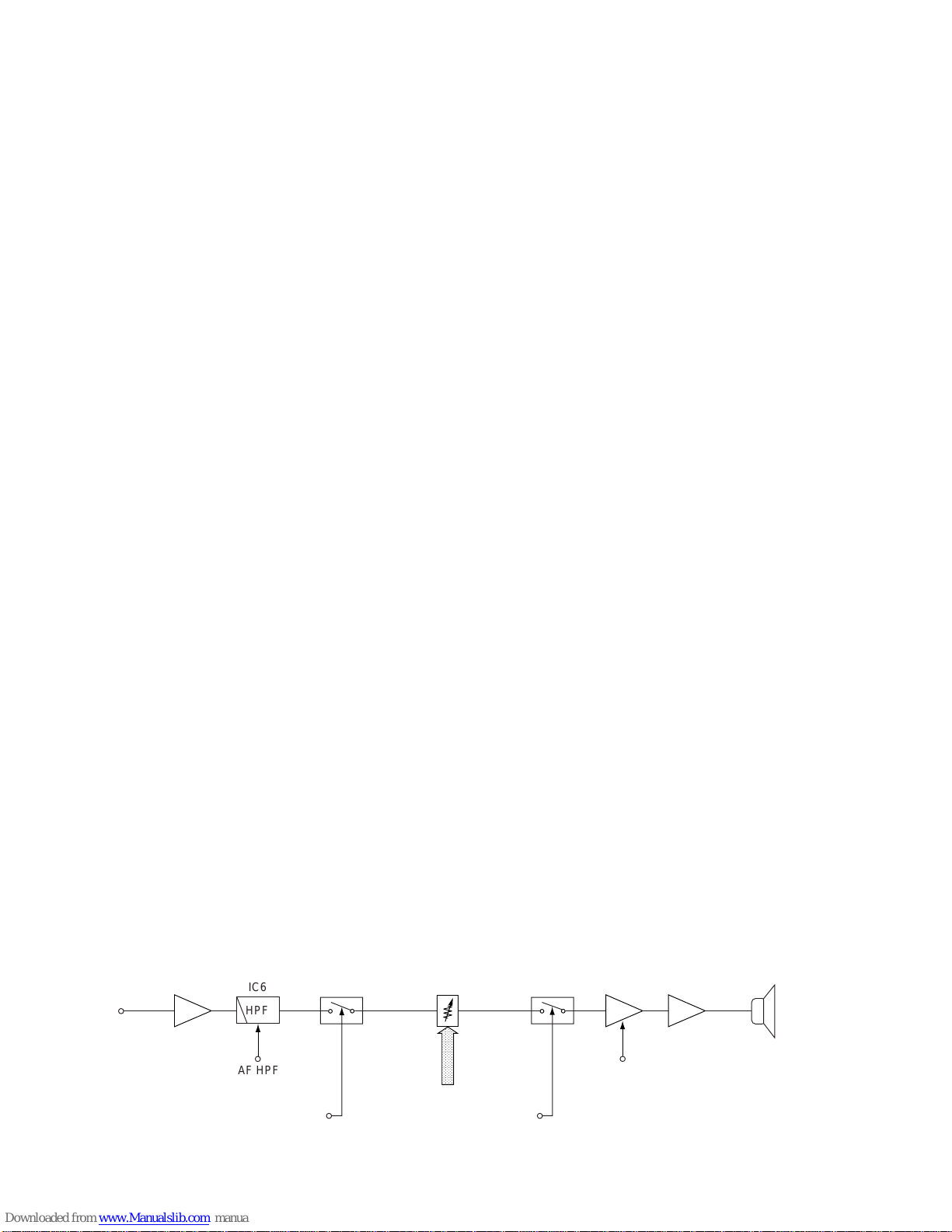
The AF amplifier circuit amplifies the demodulated AF sig-
nals to drive a speaker.
AF signals from the FM IF IC (IC1, pin 9) are amplified at the
AF amplifier (IC7a) and then pass through the high-pass fil-
ter (IC6) whose characteristics are controlled by the
“AFHPF” line. When “AFHPF” is at a high level, the cut off
frequency is shifted higher to remove CTCSS or DTCS sig-
nals.
The filtered signals from IC6 (pin 14) pass through the AF
switching IC ( IC11, pin 8, 9) and are applied to the level con-
troller (IC12, pin 16, 15). The audio level controlled signals
are again passed through the AF switching IC (IC11, pin 2,
1), applied to the de-emphasis circuit (IC4) with frequency
characteristics of –6 dB/octave, and are then power ampli-
fied at the AF amplifier (IC9) to drive a speaker.
4-1-6 RECEIVER MUTE CIRCUITS
(MAIN and FRONT units)
• NOISE SQUELCH
The noise squelch circuit cuts out AF signals when no RF
signals are received. By detecting noise components in the
AF signals, the squelch circuit switches the AF mute switch.
Aportion of the AF signals from the FM IF IC (IC1, pin 9) are
applied to the level controller (IC12, pin 24). The level con-
trolled noise components are output from pin 23 and are
applied to the active filter in IC1 (pin 8). Noise components
are amplified and output from pin 7 and are then applied to
the noise detector section (pins 10, 11). The detected noise
signals are rectified and output from pin 13 without smooth-
ing.
The noise signal (NOIS) from IC1 (pin 13) is applied to the
CPU (FRONT unit; IC1, pin 19). The CPU analyzes the
noise condition and outputs the RMUT signal via the I/O
expander IC (IC13) to toggle the AF mute switches (IC11a).
• CTCSS AND DTCS
The tone squelch circuit detects AF signals and opens the
squelch only when receiving a signal containing a matching
subaudible tone (CTCSS or DTCS). When tone squelch is in
use, and a signal with a mismatched or no subaudible tone
is received, the tone squelch circuit mutes the AF signals
even when noise squelch is open.
A portion of the AF signals from the AF amplifier (IC7b)
passes through the low-pass filter (FRONT unit; Q5) to
remove AF (voice) signals and is applied to the CTCSS or
DTCS decoder inside the CPU (FRONT unit; IC1, pin 97) via
the “CTCIN” line to control the AF mute switch via the I/O
expander IC (IC13).
4-2 TRANSMITTER CIRCUIT
4-2-1 MICROPHONE AMPLIFIER CIRCUIT
(MAIN unit)
The microphone amplifier circuit amplifies the audio signals
from the microphone, within +6 dB/octave pre-emphasis
characteristics, to a level needed for the modulation circuit.
The AF signals from the microphone are amplified at the AF
(IC8b) and limiter (IC8a) amplifiers and are then passed
through the pre-emphasis circuit (R152, C180) which has +6
dB/octave pre-emphasis characteristics.
The pre-emphasized signals are passed through the splatter
filter (IC7a) and are then applied to the AF switching IC
(IC11, pins 11, 10).
The signals are applied to the level controller (IC12, pins 16,
15). The deviation level controlled signals are passed
through the AF switching IC (IC11, pins 3, 4), and are then
applied to modulation circuit as the “MOD” signal.
The narrow/wide switch (Q35) is connected to the input of
the splatter filter (IC7a) and switched by the “NWC” signal
coming from the I/O expander IC (IC13). When “NWC” is at
a high level, the narrow/wide switch (Q35) shifts the filter
cut-off frequency for narrow deviation selection.
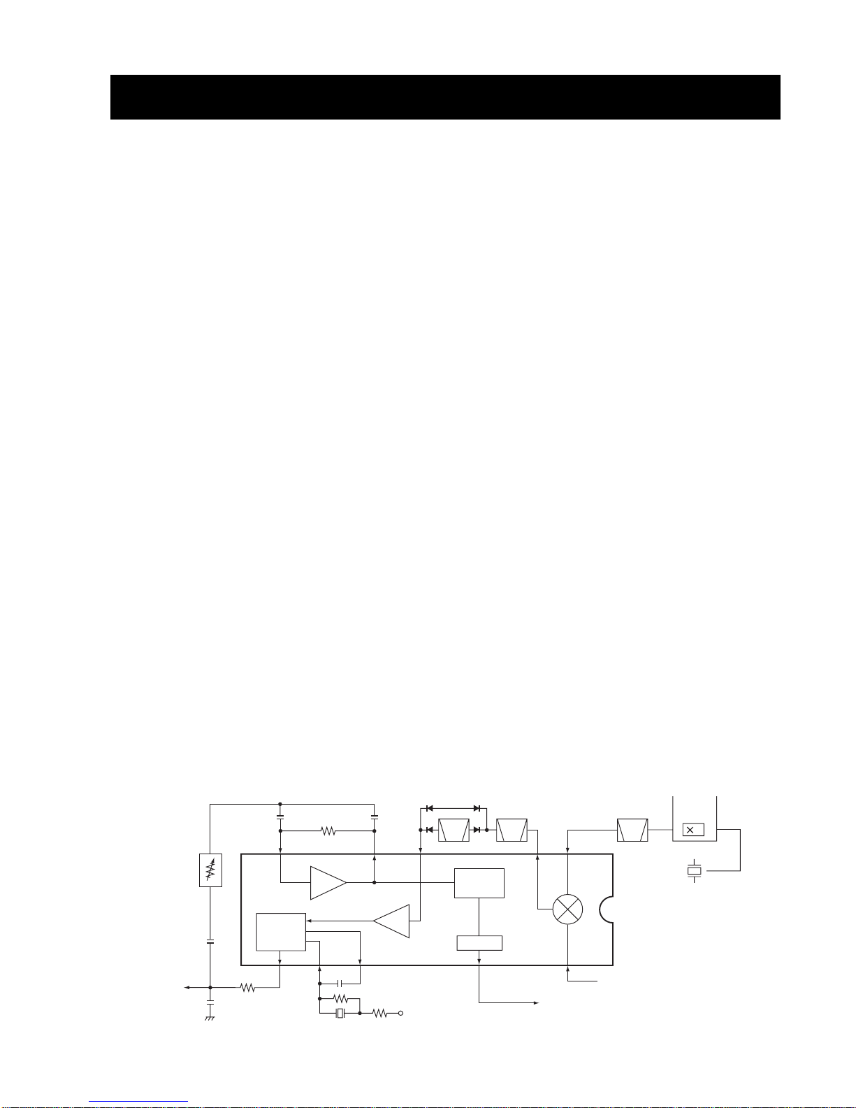
4-2-2 MODULATION CIRCUIT (MAIN unit)
The modulation circuit modulates the VCO oscillating signal
(RF signal) using the microphone AF signals.
The “MOD” signals from the AF switching IC (IC11, pin 4)
change the reactance of D21 to modulate the oscillated sig-
nal at the TX VCO circuit (Q25). The modulated signal is
amplified at the buffer amplifiers (Q28, Q30) and is then
applied to the drive amplifier circuit.
• AF circuit
Speaker
TXC RMUT
Volume control signal
Amp. Amp.
AF mute
switch AF mute
switch AF power
amp.
AF ATT
IC11c IC11a
IC12 IC4aIC7b
IC9
89
62116 15 13
AF signal
from IC1
,,,,
,,,,
,,,,
,,,,
,,,,
,,,,
,,,,
,,,,
,,,,
,,,,
,,,,
,,,,
,,,,
HPF
AF HPF
IC6

4 - 3
4-2-3 DRIVE AMPLIFIER CIRCUIT (MAIN unit)
The drive amplifier circuit amplifies the VCO oscillating sig-
nal to the level needed at the power amplifier.
The RF signal from the buffer amplifier (Q30) passes
through the T/R switch (D18) and is amplified at the buffer
(Q21, Q20) and drive (Q19) amplifiers. The amplified signal
is applied to the power amplifier circuit.
4-2-4 POWER AMPLIFIER CIRCUIT (MAIN unit)
The power amplifier circuit amplifies the driver signal to an
output power level.
The RF signal from the drive amplifier (Q19) is applied to the
power module (IC5) to obtain 35 W (for IC-F420/F420S; 25
W for IC-F410/F410S) of RF power.
The amplified signal is passed through the antenna switch-
ing circuit (D3), low-pass filter andAPC detector, and is then
applied to the antenna connector.
Collector voltages for the driver (Q19) and control voltage
for the power amplifier (IC5, pin 2) come from the APC con-
troller (Q17, Q18) to stabilize the output power. The transmit
mute switch (Q16) controls theAPC controller when transmit
mute is necessary.
4-2-5 APC CIRCUIT (MAIN unit)
The APC circuit protects the power amplifier from a mis-
matched output load and stabilizes the output power.
The APC detector circuit (D1) detects forward signals and
reflection signals. The combined voltage is at minimum level
when the antenna impedance is matched at 50 Ωand is
increased when it is mismatched.
The detected voltage is applied to the inverse amplifier
(IC4b, pin 6), and the power setting voltage (T4) is applied
to the other input (pin 5) for the reference. When antenna
impedance is mismatched, the detected voltage exceeds
the power setting voltage. The output voltage of the inverse
amplifier (IC4b, pin 7) controls the input current of the power
module (IC5) and drive amplifier (Q19) to reduce the output
power via the APC controller (Q17, Q18).
4-3 PLL CIRCUITS
4-3-1 PLL CIRCUIT
A PLL circuit provides stable oscillation of the transmit fre-
quency and receive 1st LO frequency. The PLL circuit con-
sists of the PLL IC (IC2), loop filter and reference oscillator
circuit and employs a pulse swallow counter.
An oscillated signal from the VCO (Q23, Q25) passes
through the buffer amplifiers (Q28, Q29), is applied to the
PLL IC (IC10, pin 2) and is prescaled in the PLL IC based on
the divided ratio (N-data). The reference signal is generated
at the reference oscillator (X2) and is also applied to the PLL
IC. The PLL IC detects the out-of-step phase using the ref-
erence frequency and outputs it from pin 8. The output sig-
nal is passed thorough the loop filter (Q34, R180, R181,
C203, C231) and is then applied to the VCO circuit as the
lock voltage.
4-3-2 VCO CIRCUIT (MAIN unit)
The VCO circuit contains a separate RX VCO (Q23, D20,
D34) and TX VCO (Q25, D22, D33). The oscillated signal is
amplified at the buffer amplifiers (Q28, Q29) and is then
applied to the T/R switching circuit (D18, D19). The Rx sig-
nal is applied to the 1st mixer circuit (Q3) and the Tx signal
to the driver (Q19) via the buffer amplifers (Q21, Q20).
A portion of the signal from Q28 is amplified at the buffer
amplifier (Q29) and is then fed back to the PLL IC (IC10,
pin 2).
• PLL circuit
Shift register
×3
Prescaler
Phase
detector
Loop
filter
Programmable
counter
Programmable
divider
X1
15.3 MHz
45.9 MHz signal
to the FM IF IC
15
Q23, D20, D34
RX VCO
TX VCO
Buffer
Buffer
Buffer
Q30
Q29
Q28
3
4
5PLST
IC10 (PLL IC)
SCK
SO
to transmitter circuit
to 1st mixer circuit
D19
D18
17
82
Q25, D22, D33

4-4 POWER SUPPLY CIRCUITS
4-4-1 VOLTAGE LINES (MAIN unit)
4-5 PORT ALLOCATIONS
4-5-1 CPU (FRONT unit; IC1)
CPU (IC1)—continued
4 - 4
Description
The voltage from a DC power supply.
The same voltage as the VCC line which is con-
trolled by the power switching circuit (Q14, Q15).
When the [POWER] switch is pushed, the CPU
outputs the “PWON” control signal to the power
switching circuit to turn the circuit ON.
Common 5 V for the CPU converted from the
VCC line by the CPU5V regulator circuit (IC3).
The circuit outputs the voltage regardless of the
power ON/OFF condition.
Common 8 V converted from the HV line by the
8V regulator circuit (IC2).
Common 5 V converted from the HV line by the
5V regulator circuit (Q12, Q13).
Receive 8 V controlled by the R8 regulator circuit
(Q10, Q11) using the “TXC” signal from the I/O
expander IC (IC13).
Transmit 8 V controlled by the T8 regulator circuit
(Q8, Q9) using the “TXC” signal from the I/O
expander IC (IC13).
Line
VCC
HV
CPU5V
8V
5V
R8
T8
Outputs RF attenuator control signal to
the attenuator switch
(MAIN unit; Q1).
Low : While attenuator function is ON.
Input port for PLL unlock signal from
the PLL IC (MAIN unit; IC10).
High: During unlock.
Outputs control signal for the power
switching circuit (MAIN unit; Q14, Q15).
Outputs control signal for LCD back-
light.
Low : While LCD backlight is ON.
Input port for the PTT switch from the
external connector (MAIN unit; J5).
Low : External PTT switch is ON.
Input port for the LCD backlight control
signal from the external connector
(MAIN unit; J5).
Low : External dimmer switch is ON.
Outputs strobe signals for the PLL IC
(MAIN unit; IC10).
Outputs strobe signals for the level
controller IC (MAIN unit; IC12).
Outputs strobe signals for the I/O
expander IC (MAIN unit; IC13).
Output ports for the key matrix.
Input ports for the key matrix.
Outputs control signal for the beep
mute circuit (Q10).
High: Beep muted.
Output ports for the CTCSS/ DTCS sig-
nals.
Input port for the microphone hanger
detection signal.
Low : Microphone on hook
Output port
beep audio while receiving.
2/5 tone signals while transmitting.
Outputs DTMF signals.
Input port for the option connector state
(MAIN unit; J4).
Input port for the CTCSS/DTCS
decode signals.
Input port for S-meter signal.
Input port for PLL lock voltage.
Input port for the transceiver’s internal
temperature.
32
36
37
38
39
40
41
42
43
45, 46
47–50
51
52–54
55
90
91
94–96
97
98
99
100
RFATT
UNLK
PWON
DIM
EXTPTT
DIMIN
PLST
DAST
EXST
KS1, KS0
KR3–
KR0
BM
CTDA0–
CTDA2
HANG
MTONE
TONED
OPV3–
OPV1
CTCIN
SD
LVIN
TEMP
Pin Port Description
number name
Input port for overvoltage detection
from the connected power supply.
Outputs clock signal to the EEPROM
(IC3), PLL IC (MAIN unit; IC10) and
expander ICs (MAIN unit; IC12, IC13),
etc.
Input port for the data signals from the
EEPROM (IC3), etc.
Outputs data signals to the EEPROM
(IC3), PLL IC (MAIN unit; IC10) and
expander ICs (MAIN unit; IC12, IC13),
etc.
Input port for the cloning signal.
Output port for the cloning signal.
Input for the POWER switch.
Low : While POWER switch is
pushed.
NOIS signal input port from the FM IF
IC (MAIN unit; IC1) for noise squelch
operation.
Input port for the PTT switch.
Low : While PTT switch is pushed.
1
12
13
14
16
17
18
19
26
VIN
SCK
SI
SO
CLIN
CLOUT
POSW
NOIS
PTT
Pin Port Description
number name

4 - 5
4-5-2 I/O expander IC
(1) IC12 (MAIN unit)
(2) IC13 (MAIN unit)
Output tunable band pass filter control
signals.
Output port for
tunable band pass filter control signal
while receiving.
output power control signal while
transmitting.
Output port for reference frequency
control voltage.
2, 3, 10
11
14
T1–T3
T4
REF
Pin Port Description
number name
Outputs control signal for the R8 regu-
rator circuits (MAIN unit; Q10, Q11).
High: While transmitting.
Outputs control signal for the T8 regu-
rator circuits (MAIN unit; Q8, Q9).
High: While Tx is muted.
Outputs AF mute switch (MAIN unit;
IC11) control signal for the receiver cir-
cuit.
High: While no receive audio is emit-
ed.
Outputs MIC mute control signal.
High: While DTMF signals are output,
etc.
Outputs external device control signal.
High: When matched 2/5-tone signals
are received.
Outputs control signal for the AF ampli-
fier regulator circuit.
High: When squelch is open, etc.
Outputs AF filter control signal.
High: Filters out CTCSS or DTCS fre-
quency.
Outputs receive/transmit passband
width control signal.
High: While narrow bandwidth is
selected.
4
5
6
7
11
12
13
14
TXC
TMUT
RM
MM
HORNO
AFATT
AFHPF
NWC
Pin Port Description
number name

5-1 PREPARATION
‘‘REQUIRED TEST EQUIPMENT
‘‘ADJUSTMENT FREQUENCY DATA
Before starting the adjustment, back up the original frequen-
cy data and program adjustment frequency at right using the
optional programming software (EX-2057 Rev. 1.0 or later
for IC-F410/F420, CS-F300S for IC-F410S/F420S), cloning
cable (OPC-478) and adaptor cable (OPC-592) for your con-
venience.
‘‘TRIMMER ADJUSTMENT
When you adjust the contents on page 5-4, TRIMMER
ADJUSTMENT, the optional EX-2057 (or CS-F300S), OPC-
478 and JIG CABLE (See illustration at CONNECTIONS.)
are required.
• STARTING TRIMMER ADJUSTMENT
Turn the transceiver power ON, connect a computer to the [MIC] jack using the optional OPC-478 CLONING CABLE and JIG
CABLE, then start up the "ADJUST" program in EX-2057 (or CS-F300S).
•STARTING THE PROGRAM
qBoot up DOS.
wInsert the EX-2057 (CS-F300S) backup disk into drive A.
eType the following to start up the program:
ADJ>ADJUST [/A : /B]*1[/1 : /2]*2[Enter]
• The adjustment screen appears after reading set data from
the transceiver.
rAfter the adjustment screen appears, set or modify the data as
desired.
*1PLL reference crystal type.
/A: This does not activate for IC-F410/F410S/F420/F420S’s
adjustment.
/B: TCXO crystal type. (You must select [/B] for IC-
F410/F410S/F420/F420S’s adjustment.)
*2RS-232C port number.
NOTE: When the EEPROM (FRONT unit; IC3) is replaced or the transceiver displays an error message and beeps, the
following operation is necessary before starting the ADJUSTMENT.
1. Download the programmed data using the EX-2057 or CS-F300S from an exact same version of the transceiver, then
save it. (See the instructions for detailed operation.)
2. Set the cursor to the [MODEL] and push the [↓] key on the computer keyboard.
3. Type "RESERVE" then push [Enter].
"Reserved" indicator flashes at the right hand, top corner on the computer screen.
4. Connect the transceiver which has been repaired, then write the data to the transceiver.
EQUIPMENT
DC power supply
RF power meter
(terminated type)
Frequency counter
FM deviation meter
DC voltmeter
GRADE AND RANGE
Output voltage : 13.2 (13.6) V DC
Current capacity : 15 A or more
Measuring range : 1–50 W
Frequency range : 300–600 MHz
Impedance : 50 Ω
SWR : Less than 1.2 : 1
Frequency range : 0.1–600 MHz
Frequency accuracy: ±1 ppm or better
Sensitivity : 100 mV or better
Frequency range : DC–600 MHz
Measuring range : 0 to ±10 kHz
Input impedance : 50 kΩ/V DC or better
EQUIPMENT
Audio generator
Standard signal
generator (SSG)
Oscilloscope
AC millivoltmeter
External speaker
Attenuator
GRADE AND RANGE
Frequency range : 300–3000 Hz
Measuring range : 1–500 mV
Frequency range : 0.1–600 MHz
Output level : 0.1 µV–32 mV
(–127 to –17 dBm)
Frequency range : DC–20 MHz
Measuring range : 0.01–20 V
Measuring range : 10 mV–10 V
Input impedance : 4 Ω
Capacity : 5 W or more
Power attenuation : 50 or 60 dB
Capacity : 50 W or more
• ADJUSTMENT FREQUENCY
∏∏: IC-F410/F410S (PMR), ÒÒ: IC-F420/F420S (LMR)
L: L-band, ML: ML-band, MH: MH-band, H: H-band
SECTION 5 ADJUSTMENT PROCEDURES
5 - 1
A:\>CD ADJ Boot up DOS,
and change the
directory.
Program starts up,
then the adjust-
ment screen
appears after read-
ing set data from
the transceiver.
A:\>ADJ>ADJUST [/B] [/1]
Memory CH
: 1
Power(Hi) : 174
‘ ‘ ‘ ‘ ‘ ‘ ‘ ‘ ‘ ‘ ‘ – – – – – – – – –
Power(L2) : 88
‘ ‘ ‘ ‘ ‘ ‘ ‘ – – – – – – – – – – – – – –
Power(L1) : 44
‘ ‘ ‘ – – – – – – – – – – – – – – – – – – –
M O D N : 68
‘ ‘ ‘ ‘ ‘– – – – – – – – – – – – – – – – –
M O D W : 137
‘ ‘ ‘ ‘ ‘ ‘ ‘ ‘ ‘ ‘ ‘ – – – – – – – – –
DTCS N : 24
‘ ‘ – – – – – – – – – – – – – – – – – – – –
DTCS W : 51
‘ ‘ ‘ ‘– – – – – – – – – – – – – – – – – –
TXF SET :
BPF T1 : 40
‘ ‘ ‘ ‘ ‘ – – – – – – – – – – – – – – – – –
BPF T2 : - 9
‘ ‘ ‘ ‘ – – – – – – – – – – – – – – – – – –
BPF T3 : -17
‘ ‘ ‘ ‘ – – – – – – – – – – – – – – – – – –
BPF T4 : -15
‘ ‘ ‘ ‘ ‘– – – – – – – – – – – – – – – – –
AF Vol.L : 1
– – – – – – –– – – – – – – – – – – – – – – –
S Q L : 10
‘ ‘ – – – – – – – – – – – – – – – – – – – –
∗∗∗∗∗ Trimmer Control Software for IC–F300 Series ∗∗∗∗∗ Rev. 1.0
A/D VIN 165 : A5h 13.23V
A/D TEMPS 173: ADh 24.81'C
A/D LVIN 47 : 2Fh 0.92V
A/D SD 38 : 26h 0.75V
D/A DTCS BL 149 : 95h 58.43%
D/A SQL Lev 0 : 00h 0.00%
D/A BP T1 98: 62h 2.03V
D/A BP T2 49: 31h 1.41V
D/A BP T3 41: 29h 1.31V
D/A T4/POW 43 : 2Bh 1.34V
D/A REF 147: 93h 2.40V
D/A AF/Dev 0: 00h 0.00%
RX:440.20000MHz TX:440.10000MHz MODE: Wide
POW: High
[Space]: A/D, D/A Read
[TAB]: Display Parameters [F8] at BPF: Sweep [F9] at BPF T1: Sweep T1~T4
[Enter] at TXF: REF Set Mode ↑ / ↓: Cursor Up/Down < / > : –/+ ESC : Quit
Startup command.
,
,,,
,,,,
,,,,
,,,,
,,,,
,,,
,
Channel Frequency [MHz] Power
No. L ∏∏ML ÒÒML MH ∏∏HÒÒH selection
1 400.0 440.0 450.0 470.0 490.0 Low1
2 430.0 470.0 490.0 520.0 512.0 Low1
3 400.0 440.0 450.0 470.0 490.0 Low2
4 400.0 440.0 450.0 470.0 490.0 High

5 - 2
Memory CH
: 1
Power(Hi) : 174
‘ ‘ ‘ ‘ ‘ ‘ ‘ ‘ ‘ ‘ ‘ – – – – – – – – –
Power(L2) : 88
‘ ‘ ‘ ‘ ‘ ‘ ‘ – – – – – – – – – – – – – –
Power(L1) : 44
‘ ‘ ‘ – – – – – – – – – – – – – – – – – – –
M O D N : 68
‘ ‘ ‘ ‘ ‘– – – – – – – – – – – – – – – – –
M O D W : 137
‘ ‘ ‘ ‘ ‘ ‘ ‘ ‘ ‘ ‘ ‘ – – – – – – – – –
DTCS N : 24
‘ ‘ – – – – – – – – – – – – – – – – – – – –
DTCS W : 51
‘ ‘ ‘ ‘– – – – – – – – – – – – – – – – – –
TXF SET :
BPF T1 : 40
‘ ‘ ‘ ‘ ‘ – – – – – – – – – – – – – – – – –
BPF T2 : - 9
‘ ‘ ‘ ‘ – – – – – – – – – – – – – – – – – –
BPF T3 : -17
‘ ‘ ‘ ‘ – – – – – – – – – – – – – – – – – –
BPF T4 : -15
‘ ‘ ‘ ‘ ‘– – – – – – – – – – – – – – – – –
AF Vol.L : 1
– – – – – – –– – – – – – – – – – – – – – – –
S Q L : 10
‘ ‘ – – – – – – – – – – – – – – – – – – – –
∗∗∗∗∗ Trimmer Control Software for IC–F300 Series ∗∗∗∗∗ Rev. 1.0
A/D VIN 165 : A5h 13.23V
A/D TEMPS 173: ADh 24.81'C
A/D LVIN 47 : 2Fh 0.92V
A/D SD 38 : 26h 0.75V
D/A DTCS BL 149 : 95h 58.43%
D/A SQL Lev 0 : 00h 0.00%
D/A BP T1 98: 62h 2.03V
D/A BP T2 49: 31h 1.41V
D/A BP T3 41: 29h 1.31V
D/A T4/POW 43: 2Bh 1.34V
D/A REF 147: 93h 2.40V
D/A AF/Dev 0: 00h 0.00%
RX:440.20000MHz TX:440.10000MHz MODE: Wide
POW: High
[Space]: A/D, D/A Read
[TAB]: Display Parameters [F8] at BPF: Sweep [F9] at BPF T1: Sweep T1~T4
[Enter] at TXF: REF Set Mode ↑ / ↓: Cursor Up/Down < / > : –/+ ESC : Quit
PLL lock voltage
Internal temperature
Operating channel
RF output power
FM deviation
Receive sensitivity
Reference frequency
Connected DC voltage
SQL level
DTCS balance level
Volume
Squelch
DTCS balance
The above values for settings are examples only. Each transceiver has its
own specific values for each setting.
NOTE:
‘‘PROGRAM SCREEN EXAMPLE
‘‘CONNECTIONS
FM deviation meter
(DC measurable)
Attenuator
50 dB or 60 dB
to the MIC connector
MIC connector
to the antenna connector
to DC cable
to an RS-232C port
DB9 female plug
(incl. level converter circuit)
Personal
computer
OPC-478
Pin 2 (Clone)
Pin 7 (GND)
Pin 4 (PTT)
Jig cable
Jig cable
Standard signal generator
–17 to –125 dBm
(32 mV to 0.13 µV)
CAUTION:
DO NOT transmit while
SSG is connected to
the antenna connector.
RF power meter
50 Ω/ 1–50 W
Audio generator
300 Hz to 3 kHz AC
millivoltmeter
DC power supply
13.2 (13.6) V /15 A
Frequency
counter
OPC-478
Pin 5 ( MICE)
Pin 6 ( MIC)
12345678

5 - 3
5-2 PLL ADJUSTMENT
PLL LOCK
VOLTAGE
ADJUSTMENT
ADJUSTMENT ADJUSTMENT CONDITION MEASUREMENT VALUE POINT
UNIT LOCATION UNIT ADJUST
1
2
3
4
• Operating frequency: (Ch1)
[L-band] : 400.00000 MHz
[ML-band] ∏: 440.00000 MHz
[ML-band] Ò: 450.00000 MHz
[MH-band] : 470.00000 MHz
[H-band] : 490.00000 MHz
• Receiving
• Power selection : Low1
• Transmitting
• Operating frequency: (Ch2)
[L-band] : 430.00000 MHz
[ML-band] : 470.00000 MHz
[MH-band] : 490.00000 MHz
[H-band] ∏: 520.00000 MHz
[H-band] Ò: 512.00000 MHz
• Receiving
• Power selection : Low1
• Transmitting
MAIN Connect a digital
multi-meter or oscil-
loscope to the
check point CP1.
1.5 V
1.5 V
3.5–5.5 V
MAIN L23
L26
Verify
CP1
PLL lock voltage
check point
L23
PLL lock voltage
adjustment for TX
L26
PLL lock voltage
adjustment for RX
DC power supply
13.2 (13.6) V / 15 A

5 - 4
REFERENCE
FREQUENCY
[TXF SET]
OUTPUT
POWER
[Power (Hi)]
[Power (L2)]
[Power (L1)]
FM DEVIATION
[MOD N] or
[MOD W]
ADJUSTMENT ADJUSTMENT CONDITION MEASUREMENT VALUE
UNIT LOCATION
5-3 TRIMMER ADJUSTMENT
Select an operation using [↑] / [↓] keys, then set specified value using [←] / [→] keys on the connected computer keyboard.
1
2
1
2
3
1
Rear
panel
Rear
panel
Rear
panel
Loosely couple a frequency
counter to the antenna connec-
tor.
Connect an RF power meter to
the antenna connector.
Connect an FM deviation meter
to the antenna connector
through an attenuator.
430.00000 MHz
[L-band]
470.00000 MHz
[ML-band]
490.00000 MHz
[MH-band]
520.00000 MHz
[H-band] ∏
512.00000 MHz
[H-band] Ò
430.00155 MHz
[L-band]
470.00155 MHz
[ML-band]
490.00155 MHz
[MH-band]
520.00155 MHz
[H-band] ∏
512.00155 MHz
[H-band] Ò
35.0 W [LMR]
25.0 W [PMR]
10.0 W [Italy]
20.0 W [LMR]
10.0 W [PMR]
5.0 W [Italy]
3.5 W [LMR]
2.5 W [PMR, Italy]
±4.2 kHz (Wide)
±2.1 kHz (Narrow)
NOTE:
[Wide/Narrow] ver-
sion must adjust
both setting.
• Operating frequency: (Ch2)
[L-band] : 430.00000 MHz
[ML-band] : 470.00000 MHz
[MH-band] : 490.00000 MHz
[H-band] ∏: 520.00000 MHz
[H-band] Ò: 512.00000 MHz
• Power selection : Low1
• Transmitting
• Transmitting
• Operating frequency: (Ch4)
[L-band] : 400.00000 MHz
[ML-band] ∏: 440.00000 MHz
[ML-band] Ò: 450.00000 MHz
[MH-band] : 470.00000 MHz
[H-band] : 490.00000 MHz
• Power selection : High
• Transmitting
• Power selection : Low2 (Ch3)
• Transmitting
• Power selection : Low1 (Ch1)
• Transmitting
• Operating frequency: (CH1)
[L-band] : 400.00000 MHz
[ML-band] ∏: 440.00000 MHz
[ML-band] Ò: 450.00000 MHz
[MH-band] : 470.00000 MHz
[H-band] : 490.00000 MHz
• Power selection : Low1
• Connect an audio generator to the
[MIC] jack and set as:
1 kHz / 40 mV
• Set an FM deviation meter as:
HPF : OFF
LPF : 20 kHz
De-emphasis : OFF
Detector : (P–P)/2
• Transmitting

*This output level of a standard signal generator (SSG) is indicated as SSG’s open circuit.
DTCS WAVE
FORM
RECEIVE
[BPF T1]–
[BPF T4]
SQUELCH
LEVEL
[SQL]
• Operating frequency: (CH1)
[L-band] : 400.00000 MHz
[ML-band] ∏: 440.00000 MHz
[ML-band] Ò: 450.00000 MHz
[MH-band] : 470.00000 MHz
[H-band] : 490.00000 MHz
• Connect an SSG to the antenna con-
nector and set as :
Level : adjust SSG’s level to 8
dB SINAD on the con-
necting SINAD meter
Modulation: OFF
• Receiving
CONVENIENT: The BPF T1–BPF T4 can be adjusted automatically.
q-1 Set each to 0, then push the [F9] key.
(The cursor must be set to the BPF T1 position.)
q-2 The connected PC tunes BPF T1–BPF T4 to peak levels.
or
w-1 Set the cursor to one of BPF T1, T2, T3 or T4 as desired.
w-2 Push [F8] to start tuning.
w-3 Pepeat w-1 and w-2 to perform additional BPF tuning.
• Operating frequency: (CH1)
[L-band] : 400.00000 MHz
[ML-band] ∏: 440.00000 MHz
[ML-band] Ò: 450.00000 MHz
[MH-band] : 470.00000 MHz
[H-band] : 490.00000 MHz
• Power selection : Low1
• No audio signal is applied to the [MIC]
jack
• DTCS code : 007
• Set an FM deviation meter as:
HPF : OFF
LPF : 20 kHz
De-emphasis : OFF
Detector : (P–P)/2
• Transmitting
• Operating frequency: (CH1)
[L-band] : 400.00000 MHz
[ML-band] ∏: 440.00000 MHz
[ML-band] Ò: 450.00000 MHz
[MH-band] : 470.00000 MHz
[H-band] : 490.00000 MHz
• Connect a standard signal generator to
the antenna connector and set as:
Level : 3.2 µV* (–97 dBm)
Modulation: 1 kHz
Deviation : ±3.5 kHz (Wide)
±1.75 kHz (Narrow)
• Receiving
5 - 5
ADJUSTMENT ADJUSTMENT CONDITION MEASUREMENT VALUE
UNIT LOCATION
TRIMMER ADJUSTMENT — continued
Select an operation using [↑] / [↓]keys, then set specified value using [←] / [→] keys on the connected computer keyboard.
1 Rear
panel
Rear
panel
Connect an FM deviation meter
with an oscilloscope to the
antenna connector through an
attenuator.
Connect a SINAD meter with a 4
Ωload to the external [SP] jack. Minimum distortion
level
1 Rear
panel Connect a SINAD meter with a 4
Ωload to the external [SP] jack. At the point where
noise just appears.
Set to flat wave
form

5 - 6
5-4 BEEP ADJUSTMENT
BEEP AUDIO
ADJUSTMENT
ADJUSTMENT ADJUSTMENT CONDITION MEASUREMENT VALUE POINT
UNIT LOCATION UNIT ADJUST
1 • Operating frequency: Any
• Connect an audio generator to
pin 25 (MAIN unit; J2) and set
as:
1 kHz / 550 mV
• Squelch : OPEN
• Volume level: 1
• Receiving
Rear
panel Connect an AC mil-
livoltmeter with 4 Ω
load to the [SP]
jack.
62.5 mV
FRONT
R60
DC power supply
13.2 (13.6) V / 15 A
AC
millivoltmeter
Speaker
4 Ω
SINAD
meter
Audio
generator
• MAIN unit
• FRONT unit
R60
Beep level
adjustment
J4, pin 25
Audio input point
115
16
30 25
J4
+
–

C: LCD type (F410/F420), E: LED type (F410S/F420S)
[FRONT UNIT][FRONT UNIT]
IC1 1140007911 S.IC HD6433875B20H
IC2 1110003500 S.IC S-80742SL-A6-T1
IC3 1130008670 S.IC 25LC160T-I/SN
Q1 1530002060 S.TRANSISTOR 2SC4081 T107 R
Q3 1590000440 S.TRANSISTOR DTA143ZUA T106 C
1530002060 S.TRANSISTOR 2SC4081 T107 R E
Q4 1590000660 S.TRANSISTOR DTC144TU T107
Q5 1590001650 S.TRANSISTOR XP4601 (TX)
Q6 1530002060 S.TRANSISTOR 2SC4081 T107 R
Q7 1530002060 S.TRANSISTOR 2SC4081 T107 R
Q10 1590000660 S.TRANSISTOR DTC144TU T107
Q11 1530002060 S.TRANSISTOR 2SC4081 T107 R
Q12 1530002060 S.TRANSISTOR 2SC4081 T107 R Eonly
Q13 1530002060 S.TRANSISTOR 2SC4081 T107 R Eonly
Q14 1530002060 S.TRANSISTOR 2SC4081 T107 R Eonly
Q15 1530002060 S.TRANSISTOR 2SC4081 T107 R Eonly
Q16 1530002060 S.TRANSISTOR 2SC4081 T107 R Eonly
Q17 1530002060 S.TRANSISTOR 2SC4081 T107 R Eonly
Q18 1590000430 S.TRANSISTOR DTC144EUA T106 Eonly
Q19 1590000430 S.TRANSISTOR DTC144EUA T106 Eonly
D1 1790001280 S.DIODE MA111 (TX)
D2 1750000130 S.DIODE DA204U T107
D3 1750000130 S.DIODE DA204U T107
D4 1750000130 S.DIODE DA204U T107
D5 1790000620 S.DIODE MA77 (TX)
D6 1730002320 S.ZENER MA8051-M (TX) Conly
X1 6050010150 S.XTAL CR-590 (6.8015 MHz)
L1 6200001720 S.COIL NL 322522T-1R0J
L3 6200003190 S.COIL NL 322522T-470J
R1 7030003560 S.RESISTOR ERJ3GEYJ 103 V (10 kΩ)
R2 7030003680 S.RESISTOR ERJ3GEYJ 104 V (100 kΩ)
R3 7030003720 S.RESISTOR ERJ3GEYJ 224 V (220 kΩ)
R4 7030003680 S.RESISTOR ERJ3GEYJ 104 V (100 kΩ)
R5 7030003570 S.RESISTOR ERJ3GEYJ 123 V (12 kΩ)
R6 7030003570 S.RESISTOR ERJ3GEYJ 123 V (12 kΩ)
R7 7030003800 S.RESISTOR ERJ3GEYJ 105 V (1 MΩ)
R8 7030003200 S.RESISTOR ERJ3GEYJ 100 V (10 Ω)
R11 7030003430 S.RESISTOR ERJ3GEYJ 821 V (820 Ω)Conly
R12 7030003390 S.RESISTOR ERJ3GEYJ 391 V (390 Ω)Conly
R14 7030003390 S.RESISTOR ERJ3GEYJ 391 V (390 Ω)Conly
R15 7030003480 S.RESISTOR ERJ3GEYJ 222 V (2.2 kΩ)
R16 7030003480 S.RESISTOR ERJ3GEYJ 222 V (2.2 kΩ)
R17 7410000950 S.ARRAY EXB-V8V 102JV
R18 7030003400 S.RESISTOR ERJ3GEYJ 471 V (470 Ω)
R19 7030003400 S.RESISTOR ERJ3GEYJ 471 V (470 Ω)
R20 7030003440 S.RESISTOR ERJ3GEYJ 102 V (1 kΩ)
R21 7030003440 S.RESISTOR ERJ3GEYJ 102 V (1 kΩ)
R22 7030003200 S.RESISTOR ERJ3GEYJ 100 V (10 Ω)
R24 7030003710 S.RESISTOR ERJ3GEYJ 184 V (180 kΩ)
R25 7030003650 S.RESISTOR ERJ3GEYJ 563 V (56 kΩ)
R26 7030003510 S.RESISTOR ERJ3GEYJ 392 V (3.9 kΩ)
R27 7030003630 S.RESISTOR ERJ3GEYJ 393 V (39 kΩ)
R28 7030003440 S.RESISTOR ERJ3GEYJ 102 V (1 kΩ)
R29 7030003440 S.RESISTOR ERJ3GEYJ 102 V (1 kΩ)
R30 7030003560 S.RESISTOR ERJ3GEYJ 103 V (10 kΩ)
R31 7030003560 S.RESISTOR ERJ3GEYJ 103 V (10 kΩ)
R32 7030003600 S.RESISTOR ERJ3GEYJ 223 V (22 kΩ)
R33 7030003660 S.RESISTOR ERJ3GEYJ 683 V (68 kΩ)
R34 7030003610 S.RESISTOR ERJ3GEYJ 273 V (27 kΩ)
R35 7030003560 S.RESISTOR ERJ3GEYJ 103 V (10 kΩ)
R36 7030003570 S.RESISTOR ERJ3GEYJ 123 V (12 kΩ)
R37 7030003570 S.RESISTOR ERJ3GEYJ 123 V (12 kΩ)
R38 7030003640 S.RESISTOR ERJ3GEYJ 473 V (47 kΩ)
R39 7030003680 S.RESISTOR ERJ3GEYJ 104 V (100 kΩ)
R40 7030003680 S.RESISTOR ERJ3GEYJ 104 V (100 kΩ)
R41 7030003730 S.RESISTOR ERJ3GEYJ 274 V (270 kΩ)
S.=Surface mount
R42 7030003740 S.RESISTOR ERJ3GEYJ 334 V (330 kΩ)
R43 7030003570 S.RESISTOR ERJ3GEYJ 123 V (12 kΩ)
R44 7410000950 S.ARRAY EXB-V8V 102JV
R45 7410000950 S.ARRAY EXB-V8V 102JV
R46 7410000950 S.ARRAY EXB-V8V 102JV
R47 7410000950 S.ARRAY EXB-V8V 102JV
R48 7410000950 S.ARRAY EXB-V8V 102JV
R49 7030003320 S.RESISTOR ERJ3GEYJ 101 V (100 Ω)
R50 7030003680 S.RESISTOR ERJ3GEYJ 104 V (100 kΩ)
R51 7030003440 S.RESISTOR ERJ3GEYJ 102 V (1 kΩ)
R52 7030003440 S.RESISTOR ERJ3GEYJ 102 V (1 kΩ)
R53 7030003440 S.RESISTOR ERJ3GEYJ 102 V (1 kΩ)
R54 7030003440 S.RESISTOR ERJ3GEYJ 102 V (1 kΩ)Conly
R55 7030003680 S.RESISTOR ERJ3GEYJ 104 V (100 kΩ)
R56 7030003530 S.RESISTOR ERJ3GEYJ 562 V (5.6 kΩ)
R57 7030003580 S.RESISTOR ERJ3GEYJ 153 V (15 kΩ)
R58 7030003640 S.RESISTOR ERJ3GEYJ 473 V (47 kΩ)
R59 7030003440 S.RESISTOR ERJ3GEYJ 102 V (1 kΩ)
R60 7310002740 S.TRIMMER RV-150 (RH03A3A14X0FC)103
R61 7030003680 S.RESISTOR ERJ3GEYJ 104 V (100 kΩ)
R62 7030003440 S.RESISTOR ERJ3GEYJ 102 V (1 kΩ)
R63 7030003440 S.RESISTOR ERJ3GEYJ 102 V (1 kΩ)
R64 7030003440 S.RESISTOR ERJ3GEYJ 102 V (1 kΩ)
R65 7030003680 S.RESISTOR ERJ3GEYJ 104 V (100 kΩ)Conly
R66 7030003680 S.RESISTOR ERJ3GEYJ 104 V (100 kΩ)Conly
R67 7030003680 S.RESISTOR ERJ3GEYJ 104 V (100 kΩ)Conly
R68 7030003640 S.RESISTOR ERJ3GEYJ 473 V (47 kΩ)
R69 7030003680 S.RESISTOR ERJ3GEYJ 104 V (100 kΩ)
R70 7030003640 S.RESISTOR ERJ3GEYJ 473 V (47 kΩ)
R71 7030003440 S.RESISTOR ERJ3GEYJ 102 V (1 kΩ)Eonly
R72 7030003400 S.RESISTOR ERJ3GEYJ 471 V (470 Ω)Eonly
R73 7030003470 S.RESISTOR ERJ3GEYJ 182 V (1.8 kΩ)Eonly
R74 7030003470 S.RESISTOR ERJ3GEYJ 182 V (1.8 kΩ)Eonly
R75 7030003470 S.RESISTOR ERJ3GEYJ 182 V (1.8 kΩ)Eonly
R76 7030003470 S.RESISTOR ERJ3GEYJ 182 V (1.8 kΩ)Eonly
R77 7030003470 S.RESISTOR ERJ3GEYJ 182 V (1.8 kΩ)Eonly
R78 7030003650 S.RESISTOR ERJ3GEYJ 563 V (56 kΩ)Eonly
R79 7030003630 S.RESISTOR ERJ3GEYJ 393 V (39 kΩ)Eonly
R80 7030003680 S.RESISTOR ERJ3GEYJ 104 V (100 kΩ)Eonly
R81 7030003680 S.RESISTOR ERJ3GEYJ 104 V (100 kΩ)Eonly
R82 7030003680 S.RESISTOR ERJ3GEYJ 104 V (100 kΩ)Eonly
R83 7030003680 S.RESISTOR ERJ3GEYJ 104 V (100 kΩ)Eonly
R84 7030003680 S.RESISTOR ERJ3GEYJ 104 V (100 kΩ)Eonly
R85 7030003440 S.RESISTOR ERJ3GEYJ 102 V (1 kΩ)Eonly
R86 7030003440 S.RESISTOR ERJ3GEYJ 102 V (1 kΩ)Eonly
R87 7030003430 S.RESISTOR ERJ3GEYJ 821 V (820 Ω)Eonly
C1 4030006900 S.CERAMIC C1608 JB 1E 103K-T-A
C2 4030006900 S.CERAMIC C1608 JB 1E 103K-T-A
C3 4030006900 S.CERAMIC C1608 JB 1E 103K-T-A
C4 4030006900 S.CERAMIC C1608 JB 1E 103K-T-A
C5 4030006900 S.CERAMIC C1608 JB 1E 103K-T-A
C6 4030006900 S.CERAMIC C1608 JB 1E 103K-T-A
C7 4030006900 S.CERAMIC C1608 JB 1E 103K-T-A
C8 4030006900 S.CERAMIC C1608 JB 1E 103K-T-A
C9 4550006200 S.TANTALUM ECST0JY106R
C10 4030006900 S.CERAMIC C1608 JB 1E 103K-T-A
C11 4030006860 S.CERAMIC C1608 JB 1H 102K-T-A
C12 4030006900 S.CERAMIC C1608 JB 1E 103K-T-A
C13 4030006860 S.CERAMIC C1608 JB 1H 102K-T-A
C14 4550006140 S.TANTALUM ECST1EY474R
C15 4030006860 S.CERAMIC C1608 JB 1H 102K-T-A
C16 4030006860 S.CERAMIC C1608 JB 1H 102K-T-A
C17 4030006860 S.CERAMIC C1608 JB 1H 102K-T-A
C18 4030007090 S.CERAMIC C1608 CH 1H 470J-T-A
C19 4030009920 S.CERAMIC C1608 CH 1H 050B-T-A
C20 4030009990 S.CERAMIC C1608 CH 1H 200J-T-A
6 - 1
SECTION 6 PARTS LIST
REF ORDER DESCRIPTION
NO. NO. REF ORDER DESCRIPTION
NO. NO.

[FRONT UNIT]
S.=Surface mount
C: LCD type (F410/F420), E: LED type (F410S/F420S)
W1 7030000010 S.JUMPER MCR10EZHJ JPW (000)
W2 7030003860 S.JUMPER ERJ3GE JPW V
W3 8900007680 CABLE OPC-741
EP1 0910049322 PCB B 5042B C
0910051231 PCB B 5289A E
EP2 8930044930 LCD CONTACT SRCN-2055-SP-N-W Conly
[FRONT UNIT]
C21 4030006900 S.CERAMIC C1608 JB 1E 103K-T-A
C22 4030007090 S.CERAMIC C1608 CH 1H 470J-T-A
C23 4030007090 S.CERAMIC C1608 CH 1H 470J-T-A
C24 4030007090 S.CERAMIC C1608 CH 1H 470J-T-A
C25 4030007090 S.CERAMIC C1608 CH 1H 470J-T-A
C26 4030007090 S.CERAMIC C1608 CH 1H 470J-T-A
C27 4030007090 S.CERAMIC C1608 CH 1H 470J-T-A
C28 4030006860 S.CERAMIC C1608 JB 1H 102K-T-A
C29 4030006860 S.CERAMIC C1608 JB 1H 102K-T-A
C30 4030006850 S.CERAMIC C1608 JB 1H 471K-T-A
C32 4030006860 S.CERAMIC C1608 JB 1H 102K-T-A
C33 4030006860 S.CERAMIC C1608 JB 1H 102K-T-A
C34 4030007090 S.CERAMIC C1608 CH 1H 470J-T-A
C35 4030006860 S.CERAMIC C1608 JB 1H 102K-T-A
C36 4030006900 S.CERAMIC C1608 JB 1E 103K-T-A
C37 4550006700 S.TANTALUM ECST1AY106R
C38 4030008880 S.CERAMIC C1608 JB 1C 223K-T-A
C39 4030011600 S.CERAMIC C1608 JB 1C 104KT-N
C40 4030008920 S.CERAMIC C1608 JB 1C 473K-T-A
C41 4030008900 S.CERAMIC C1608 JB 1C 333K-T-A
C42 4030011600 S.CERAMIC C1608 JB 1C 104KT-N
C43 4030006900 S.CERAMIC C1608 JB 1E 103K-T-A
C44 4030006900 S.CERAMIC C1608 JB 1E 103K-T-A
C45 4030006900 S.CERAMIC C1608 JB 1E 103K-T-A
C46 4030007090 S.CERAMIC C1608 CH 1H 470J-T-A
C47 4030007090 S.CERAMIC C1608 CH 1H 470J-T-A
C48 4030007090 S.CERAMIC C1608 CH 1H 470J-T-A
C49 4030007090 S.CERAMIC C1608 CH 1H 470J-T-A
C50 4030007090 S.CERAMIC C1608 CH 1H 470J-T-A
C52 4030007090 S.CERAMIC C1608 CH 1H 470J-T-A
C56 4030007090 S.CERAMIC C1608 CH 1H 470J-T-A
C57 4030007090 S.CERAMIC C1608 CH 1H 470J-T-A
C58 4030007090 S.CERAMIC C1608 CH 1H 470J-T-A
C59 4030007090 S.CERAMIC C1608 CH 1H 470J-T-A
C60 4030007090 S.CERAMIC C1608 CH 1H 470J-T-A
C61 4030007090 S.CERAMIC C1608 CH 1H 470J-T-A
C62 4030007090 S.CERAMIC C1608 CH 1H 470J-T-A
C63 4030007090 S.CERAMIC C1608 CH 1H 470J-T-A
C64 4030007090 S.CERAMIC C1608 CH 1H 470J-T-A
C65 4030007090 S.CERAMIC C1608 CH 1H 470J-T-A
C66 4030007090 S.CERAMIC C1608 CH 1H 470J-T-A
C67 4030006860 S.CERAMIC C1608 JB 1H 102K-T-A
C69 4030006860 S.CERAMIC C1608 JB 1H 102K-T-A
C70 4030007090 S.CERAMIC C1608 CH 1H 470J-T-A
C71 4030007090 S.CERAMIC C1608 CH 1H 470J-T-A
C73 4030007090 S.CERAMIC C1608 CH 1H 470J-T-A
C74 4030007090 S.CERAMIC C1608 CH 1H 470J-T-A
C77 4030007090 S.CERAMIC C1608 CH 1H 470J-T-A
C78 4030007090 S.CERAMIC C1608 CH 1H 470J-T-A
C79 4030007090 S.CERAMIC C1608 CH 1H 470J-T-A
C80 4030007090 S.CERAMIC C1608 CH 1H 470J-T-A
C82 4030011600 S.CERAMIC C1608 JB 1C 104KT-N
C83 4030006860 S.CERAMIC C1608 JB 1H 102K-T-A Eonly
C84 4030006860 S.CERAMIC C1608 JB 1H 102K-T-A Eonly
C85 4030006860 S.CERAMIC C1608 JB 1H 102K-T-A Eonly
C86 4030006860 S.CERAMIC C1608 JB 1H 102K-T-A Eonly
C87 4030006860 S.CERAMIC C1608 JB 1H 102K-T-A Eonly
C88 4030006860 S.CERAMIC C1608 JB 1H 102K-T-A Eonly
C89 4030006860 S.CERAMIC C1608 JB 1H 102K-T-A Eonly
C90 4030006860 S.CERAMIC C1608 JB 1H 102K-T-A Eonly
C92 4030007090 S.CERAMIC C1608 CH 1H 470J-T-A Eonly
J1 6450001470 CONNECTOR 95003-2881
J2 6510020510 S.CONNECTOR FH12-40S-0.5SV
DS1 5030001540 LCD LD-HU10140J Conly
DS2 5040002310 S.LED SML-311YTT86 Conly
DS3 5040002310 S.LED SML-311YTT86 Conly
DS4 5040002310 S.LED SML-311YTT86 Conly
DS5 5040002310 S.LED SML-311YTT86 Conly
DS6 5040002310 S.LED SML-311YTT86 Conly
DS7 5040002310 S.LED SML-311YTT86 Conly
DS8 5040002310 S.LED SML-311YTT86
DS9 5040002310 S.LED SML-311YTT86
DS10 5040002310 S.LED SML-311YTT86
DS11 5040002310 S.LED SML-311YTT86
DS12 5040001760 S.LED SEC 2422C Eonly
DS13 5040002310 S.LED SML-311YTT86 Eonly
DS14 5040002310 S.LED SML-311YTT86 Eonly
DS15 5040002310 S.LED SML-311YTT86 Eonly
DS16 5040002310 S.LED SML-311YTT86 Eonly
DS17 5040002310 S.LED SML-311YTT86 Eonly
6 - 2
REF ORDER DESCRIPTION
NO. NO. REF ORDER DESCRIPTION
NO. NO.

∏: PMR, Ò: LMR
[MAIN UNIT][MAIN UNIT]
S.=Surface mount
IC1 1110003490 S.IC TA31136FN (D,EL)
IC2 1180001250 S.IC TA7808F (TE16L)
IC3 1180000970 S.IC AN78L05M-(E1)
IC4 1110002700 S.IC NJM2904M-T1
IC5 1150001670 IC S-AU27AL/SC-1322 ∏[L-band]
1150001680 IC S-AU27AM/SC-1323
∏[ML/[MH-band]
1150001690 IC S-AU27AH/SC-1324 ∏[H-band]
1150001250 IC M57788L/SC1236 Ò[L-band]
1150001260 IC M57788H/SC1237 Ò[ML-band]
1150001700 IC M57788UH/SC1325 Ò[MH-band]
1150001710 IC M57788SH/SC1326 Ò[H-band]
IC6 1110002680 S.IC NJM2902M-T1
IC7 1110002700 S.IC NJM2904M-T1
IC8 1110002700 S.IC NJM2904M-T1
IC9 1110003090 IC LA4425A
IC10 1130007610 S.IC µPD3140GS-E1 (DS8)
IC11 1130007690 S.IC BU4066BCF-T1
IC12 1190000350 S.IC M62363FP-650C
IC13 1130007700 S.IC BU4094BCF-T1
Q1 1590000720 S.TRANSISTOR DTA144EUA T106
Q2 1580000660 S.FET 3SK272-(TX)
Q3 1580000680 S.FET 3SK241-R (TX)
Q4 1530002600 S.TRANSISTOR 2SC4215-O (TE85R)
Q5 1530002060 S.TRANSISTOR 2SC4081 T107 R
Q7 1590000720 S.TRANSISTOR DTA144EUA T106
Q8 1540000550 S.TRANSISTOR 2SD1664 T100Q
Q9 1590000680 S.TRANSISTOR DTC114EUA T106
Q10 1540000550 S.TRANSISTOR 2SD1664 T100Q
Q11 1590000680 S.TRANSISTOR DTC114EUA T106
Q12 1520000460 S.TRANSISTOR 2SB1132 T100 R
Q13 1590001190 S.TRANSISTOR XP6501-(TX) .AB
Q14 1550000020 S.FET 2SJ377 (TE16R)
Q15 1590000680 S.TRANSISTOR DTC114EUA T106
Q16 1590000430 S.TRANSISTOR DTC144EUA T106
Q17 1530002060 S.TRANSISTOR 2SC4081 T107 R
Q18 1520000380 TRANSISTOR 2SB1143 S
Q19 1530003291 S.TRANSISTOR 2SC4703-T1 SE
Q20 1530003310 S.TRANSISTOR 2SC5107-O (TE85R)
Q21 1530003310 S.TRANSISTOR 2SC5107-O (TE85R)
Q22 1530002060 S.TRANSISTOR 2SC4081 T107 R
Q23 1530003420 S.TRANSISTOR 2SC5110-O (TE85R)
Q24 1590000680 S.TRANSISTOR DTC114EUA T106
Q25 1530003420 S.TRANSISTOR 2SC5110-O (TE85R)
Q26 1590000680 S.TRANSISTOR DTC114EUA T106
Q27 1590000430 S.TRANSISTOR DTC144EUA T106
Q28 1530003310 S.TRANSISTOR 2SC5107-O (TE85R)
Q29 1530003310 S.TRANSISTOR 2SC5107-O (TE85R)
Q30 1530003420 S.TRANSISTOR 2SC5110-O (TE85R)
Q31 1530002060 S.TRANSISTOR 2SC4081 T107 R
Q32 1590000430 S.TRANSISTOR DTC144EUA T106
Q33 1560000530 S.FET 2SK880-GR (TE85R)
Q34 1560000400 S.FET 2SK536-TA
Q35 1530002060 S.TRANSISTOR 2SC4081 T107 R
Q36 1590000430 S.TRANSISTOR DTC144EUA T106
Q37 1590000430 S.TRANSISTOR DTC144EUA T106
Q38 1590000430 S.TRANSISTOR DTC144EUA T106
Q39 1590000430 S.TRANSISTOR DTC144EUA T106
Q40 1590001450 S.FET 2SJ144-GR (TE85R)
Q41 1590000990 S.TRANSISTOR DTC363EK T147
Q42 1590000430 S.TRANSISTOR DTC144EUA T106
Q44 1590000430 S.TRANSISTOR DTC144EUA T106
Q45 1590000720 S.TRANSISTOR DTA144EUA T106
Q46 1590000720 S.TRANSISTOR DTA144EUA T106
D1 1790000650 S.DIODE MA713 (TX)
D3 1750000510 S.DIODE UM9401F ∏
1710000310 DIODE MI407 Ò
D4 1710000730 S.DIODE MI809-T11
D5 1790000620 S.DIODE MA77 (TX)
D6 1750000260 S.DIODE 1SS352 (TPH3)
D7 1720000370 S.VARICAP HVU350TRF
D8 1720000370 S.VARICAP HVU350TRF
D9 1720000370 S.VARICAP HVU350TRF
D10 1720000370 S.VARICAP HVU350TRF
D12 1160000060 S.DIODE DAN202U T107
D13 1160000060 S.DIODE DAN202U T107
D14 1750000300 S.DIODE 1SS302 (TE85R)
D15 1750000300 S.DIODE 1SS302 (TE85R)
D16 1790000700 DIODE DSA3A1
D17 1750000370 S.DIODE DA221 TL
D18 1790000620 S.DIODE MA77 (TX)
D19 1790000620 S.DIODE MA77 (TX)
D20 1720000370 S.VARICAP HVU350TRF
D21 1720000520 S.VARICAP 1T365-01-T8A
D22 1720000370 S.VARICAP HVU350TRF
D23 1790001280 S.DIODE MA111 (TX)
D24 1160000060 S.DIODE DAN202U T107
D25 1790001280 S.DIODE MA111 (TX)
D27 1790001280 S.DIODE MA111 (TX)
D28 1730000520 ZENER RD20E B2
D29 1160000060 S.DIODE DAN202U T107
D30 1790001280 S.DIODE MA111 (TX)
D31 1160000060 S.DIODE DAN202U T107
D32 1790001280 S.DIODE MA111 (TX)
D33 1720000370 S.VARICAP HVU350TRF
D34 1720000370 S.VARICAP HVU350TRF
FI1 2010002230 XTAL FL-287 (46.350 MHz)
FI2 2020001270 CERAMIC CFWM450E
FI3 2020001410 CERAMIC CFWM450G
X1 6070000210
S.DISCRIMINATOR
CDBCA450CX24
X2 6050010230 S.XTAL CR-601 (15.300 MHz)
L1 6110002110 COIL LA-382 [H-band]
6110001520 COIL LA-232 other
L2 6110002110 COIL LA-382 [H-band]
6110001520 COIL LA-232 other
L3 6110002110 COIL LA-382
L4 6200005800 S.COIL 33CS-Y655LY-02M=P3 [H-band]
6200005780 S.COIL 33CS-Y655LY-03K=P3 other
L5 6200005780 S.COIL 33CS-Y655LY-03K=P3
L6 6170000230 COIL LW-25
L7 6200002330 S.COIL LQN 1A 15NJ04
L8 6200002330 S.COIL LQN 1A 15NJ04
L9 6200004440 S.COIL ELJFC 4R7M-F
L10 6200002330 S.COIL LQN 1A 15NJ04
L11 6200002330 S.COIL LQN 1A 15NJ04
L12 6200005730 S.COIL ELJRE 39NG-F
L13 6200003290 S.COIL ELJNC R12K-F
L14 6200002150 S.COIL ELJNC 56NK-F
L15 6200002520 S.COIL ELJNC R18K-F
L16 6110001590 COIL LA-242[L/ML-band], Ò[MH-band]
6110001520 COIL LA-232 ∏[MH-band], [H-band]
L17 6200005690 S.COIL ELJRE 18NG-F
L18 6200005700 S.COIL ELJRE 22NG-F
L19 6200005680 S.COIL ELJRE 15NG-F
L20 6200005690 S.COIL ELJRE 18NG-F
L21 6200005690 S.COIL ELJRE 18NG-F [H-band]
6200005700 S.COIL ELJRE 22NG-F other
L22 6200004230 S.COIL ELJNC R56K-F
L23 6200003690 S.COIL MC152-E558ANA-100051=P3
L24 6200001620 S.COIL ELJFC 1R0K-F
L25 6200002520 S.COIL ELJNC R18K-F
L26 6200003690 S.COIL MC152-E558ANA-100051=P3
[L/ML-band]
6200004110 S.COIL MC152-E558ANA-100050
[MH/H-band]
L27 6200001620 S.COIL ELJFC 1R0K-F
L28 6200005710 S.COIL ELJRE 27NG-F
L30 6200005710 S.COIL ELJRE 27NG-F
L31 6200005690 S.COIL ELJRE 18NG-F
L32 6200004230 S.COIL ELJNC R56K-F
L33 6200004230 S.COIL ELJNC R56K-F
L34 6200005690 S.COIL ELJRE 18NG-F
R1 7030000620 S.RESISTOR MCR10EZHJ 100 kΩ
R2 7030003320 S.RESISTOR ERJ3GEYJ 101 V (100 Ω)
R3 7030003320 S.RESISTOR ERJ3GEYJ 101 V (100 Ω)
R4 7030000220 S.RESISTOR MCR10EZHJ 47 Ω(470)
R5 7030003320 S.RESISTOR ERJ3GEYJ 101 V (100 Ω)
R6 7030003320 S.RESISTOR ERJ3GEYJ 101 V (100 Ω)
R7 7030000220 S.RESISTOR MCR10EZHJ 47 Ω(470)
R8 7030001170 S.RESISTOR MCR50JZHJ 220 Ω(221)
R9 7030001170 S.RESISTOR MCR50JZHJ 220 Ω(221)
6 - 3
REF ORDER DESCRIPTION
NO. NO. REF ORDER DESCRIPTION
NO. NO.
This manual suits for next models
3
Table of contents
Other Icom Transceiver manuals