Icom IC-M601 User manual

VHF MARINE TRANSCEIVER
iM601
SERVICE
MANUAL

INTRODUCTION
This service manual describes the latest service information
for the IC-M601 VHF MARINE TRANSCEIVER at the time of
publication.
DANGER
NEVER connect the transceiver to an AC outlet or to a DC
power supply that uses more than 15.8 V. This will ruin the
transceiver.
DO NOT expose the transceiver to rain, snow or any liquids.
DO NOT reverse the polarities of the power supply when con-
necting the transceiver.
DO NOT apply an RF signal of more than 20 dBm (100 mW)
to the antenna connector. This could damage the transceiv-
er’s front end.
ORDERING PARTS
Be sure to include the following four points when ordering
replacement parts:
1. 10-digit order numbers
2. Component part number and name
3. Equipment model name and unit name
4. Quantity required
<SAMPLE ORDER>
1110003490 S.IC TA31136FN IC-M601 MAIN UNIT 5 pieces
8820001210 Screw 2438 screw IC-M601 Top cover 10 pieces
Addresses are provided on the inside back cover for your
convenience.
REPAIR NOTES
1. Make sure a problem is internal before disassembling the
transceiver.
2. DO NOT open the transceiver until the transceiver is
disconnected from its power source.
3. DO NOT force any of the variable components. Turn
them slowly and smoothly.
4. DO NOT short any circuits or electronic parts. An insu-
lated tuning tool MUST be used for all adjustments.
5. DO NOT keep power ON for a long time when the trans-
ceiver is defective.
6. DO NOT transmit power into a signal generator or a
sweep generator.
7. ALWAYS connect a 50 dB to 60 dB attenuator between
the transceiver and a deviation meter or spectrum ana-
lyzer when using such test equipment.
8. READ the instructions of test equipment thoroughly
before connecting equipment to the transceiver.
To upgrade quality, any electrical or mechanical parts and
internal circuits are subject to change without notice or
obligation.
MODEL
IC-M601
VERSION
United Kingdom
Europe
Holland
Germany
SYMBOL
UK
EUR
HOL
FRG

TABLE OF CONTENTS
SECTION 1 SPECIFICATIONS
SECTION 2 INSIDE VIEWS
2 - 1 IC-M601 . . . . . . . . . . . . . . . . . . . . . . . . . . . . . . . . . . . . . . . . . . . . . . . . . . . . . . . . . . . . . . . . . . . . . . 2 - 1
2 - 2 HM-134 (OPTIONAL UNIT) . . . . . . . . . . . . . . . . . . . . . . . . . . . . . . . . . . . . . . . . . . . . . . . . . . . . . . . . 2 - 2
SECTION 3 DISASSEMBLY INSTRUCTION
SECTION 4 CIRCUIT DESCRIPTION
4 - 1 RECEIVER CIRCUITS . . . . . . . . . . . . . . . . . . . . . . . . . . . . . . . . . . . . . . . . . . . . . . . . . . . . . . . . . . . . 4 - 1
4 - 2 TRANSMITTER CIRCUITS . . . . . . . . . . . . . . . . . . . . . . . . . . . . . . . . . . . . . . . . . . . . . . . . . . . . . . . . 4 - 3
4 - 3 PLL CIRCUITS . . . . . . . . . . . . . . . . . . . . . . . . . . . . . . . . . . . . . . . . . . . . . . . . . . . . . . . . . . . . . . . . . 4 - 4
4 - 4 DSC CIRCUITS . . . . . . . . . . . . . . . . . . . . . . . . . . . . . . . . . . . . . . . . . . . . . . . . . . . . . . . . . . . . . . . . 4 - 5
4 - 5 LOGIC CIRCUITS . . . . . . . . . . . . . . . . . . . . . . . . . . . . . . . . . . . . . . . . . . . . . . . . . . . . . . . . . . . . . . . 4 - 5
4 - 6 POWER SUPPLY CIRCUITS . . . . . . . . . . . . . . . . . . . . . . . . . . . . . . . . . . . . . . . . . . . . . . . . . . . . . . 4 - 6
4 - 7 PORT ALLOCATIONS . . . . . . . . . . . . . . . . . . . . . . . . . . . . . . . . . . . . . . . . . . . . . . . . . . . . . . . . . . . . 4 - 6
SECTION 5 ADJUSTMENT PROCEDURES
5 - 1 PREPARATION . . . . . . . . . . . . . . . . . . . . . . . . . . . . . . . . . . . . . . . . . . . . . . . . . . . . . . . . . . . . . . . . . 5 - 1
5 - 2 PLL ADJUSTMENTS . . . . . . . . . . . . . . . . . . . . . . . . . . . . . . . . . . . . . . . . . . . . . . . . . . . . . . . . . . . . . 5 - 2
5 - 3 RECEIVER ADJUSTMENTS . . . . . . . . . . . . . . . . . . . . . . . . . . . . . . . . . . . . . . . . . . . . . . . . . . . . . . . 5 - 3
SECTION 6 PARTS LIST
SECTION 7 MECHANICAL PARTS
7 - 1 IC-M601 . . . . . . . . . . . . . . . . . . . . . . . . . . . . . . . . . . . . . . . . . . . . . . . . . . . . . . . . . . . . . . . . . . . . . . 7 - 1
7 - 2 HM-137 . . . . . . . . . . . . . . . . . . . . . . . . . . . . . . . . . . . . . . . . . . . . . . . . . . . . . . . . . . . . . . . . . . . . . . . 7 - 3
7 - 3 HM-134 (OPTIONAL UNIT) . . . . . . . . . . . . . . . . . . . . . . . . . . . . . . . . . . . . . . . . . . . . . . . . . . . . . . . . 7 - 3
SECTION 8 SEMI-CONDUCTOR INFORMATION
SECTION 9 BOARD LAYOUTS
9 - 1 VR BOARD . . . . . . . . . . . . . . . . . . . . . . . . . . . . . . . . . . . . . . . . . . . . . . . . . . . . . . . . . . . . . . . . . . . . 9 - 1
9 - 2 SQL BOARD . . . . . . . . . . . . . . . . . . . . . . . . . . . . . . . . . . . . . . . . . . . . . . . . . . . . . . . . . . . . . . . . . . . 9 - 1
9 - 3 DIAL BOARD . . . . . . . . . . . . . . . . . . . . . . . . . . . . . . . . . . . . . . . . . . . . . . . . . . . . . . . . . . . . . . . . . . . 9 - 1
9 - 4 CONNECT-A UNIT . . . . . . . . . . . . . . . . . . . . . . . . . . . . . . . . . . . . . . . . . . . . . . . . . . . . . . . . . . . . . . 9 - 1
9 - 5 LOGIC BOARD . . . . . . . . . . . . . . . . . . . . . . . . . . . . . . . . . . . . . . . . . . . . . . . . . . . . . . . . . . . . . . . . . 9 - 2
9 - 6 MAIN UNIT . . . . . . . . . . . . . . . . . . . . . . . . . . . . . . . . . . . . . . . . . . . . . . . . . . . . . . . . . . . . . . . . . . . . 9 - 4
9 - 7 AF UNIT . . . . . . . . . . . . . . . . . . . . . . . . . . . . . . . . . . . . . . . . . . . . . . . . . . . . . . . . . . . . . . . . . . . . . . 9 - 6
9 - 8 HM-137 . . . . . . . . . . . . . . . . . . . . . . . . . . . . . . . . . . . . . . . . . . . . . . . . . . . . . . . . . . . . . . . . . . . . . . . 9 - 8
9 - 9 HM-134 (OPTIONAL UNIT) . . . . . . . . . . . . . . . . . . . . . . . . . . . . . . . . . . . . . . . . . . . . . . . . . . . . . . . . 9 - 8
SECTION 10 BLOCK DIAGRAM
SECTION 11 WIRING DIAGRAM
SECTION 12 VOLTAGE DIAGRAM
12 - 1 LOGIC BOARD . . . . . . . . . . . . . . . . . . . . . . . . . . . . . . . . . . . . . . . . . . . . . . . . . . . . . . . . . . . . . . . . 12 - 1
12 - 2 MAIN UNIT . . . . . . . . . . . . . . . . . . . . . . . . . . . . . . . . . . . . . . . . . . . . . . . . . . . . . . . . . . . . . . . . . . . 12 - 2
12 - 3 AF UNIT . . . . . . . . . . . . . . . . . . . . . . . . . . . . . . . . . . . . . . . . . . . . . . . . . . . . . . . . . . . . . . . . . . . . . 12 - 4
12 - 4 HM-137 . . . . . . . . . . . . . . . . . . . . . . . . . . . . . . . . . . . . . . . . . . . . . . . . . . . . . . . . . . . . . . . . . . . . . 12 - 5
12 - 5 HM-134 (OPTIONAL UNIT) . . . . . . . . . . . . . . . . . . . . . . . . . . . . . . . . . . . . . . . . . . . . . . . . . . . . . . . 12 - 6

SECTION 1 SPECIFICATIONS
1 - 1
‘‘GENERAL
• Frequency coverage : 156.000–161.450 MHz (Tx)
156.000–163.425 MHz (Rx)
• Mode : 16K0G3E (FM) / 16K0G2B (DSC)*3
• Usable channels : All international and U.S.A channels [UK]
: All international channel only [EUR]
: All international and ATIS channels [HOL]
: All international, DSC and ATIS channels [FRG]
• Power supply requirement : 10.8 V–15.6V (negative ground)
• Usable temperature range : –20˚C to +60˚C
• +Frequency stability : Less than ±1.5 kHz (–20˚C to +60˚C)
• Current drain (at 13.8 V DC) : Transmit at 25 W 5.5 A
Receive max. audio 1.5 A
• Antenna connector : SO-239 (50 Ω)
• Dimensions (projections not included) : 220(W)×110(H)×109.4(D) mm; 821⁄32(W) ×411⁄32(H) ×45⁄16(D) inch
•Weight : 1350 g; 2.97 lb
‘‘TRANSMITTER
•Output power (at 13.8 V DC) : High 25 W
Low 1 W
•Modulation : Variable reactance frequency modulation
•Maximum frequency deviation : ±5.0 kHz
•Frequency error : Less than ±0.3 kHz
•Spurious emissions : Less than 0.25 µV
•Adjacent channel power : More than 70 dB
•Residual modulation : More than 40 dB
•Audio harmonic distortion : Less than 10% at 60% deviation
•Audio frequency response : +1 dB to –3 dB of 6 dB octave from 300 Hz to 3000 Hz
•Microphone impedance : 2 kΩ
‘‘RECEIVER
•Receive system : Double conversion superheterodyne system
•Intermediate frequencies : 1st 21.7 MHz*1, 31.05 MHz*2
2nd 450 kHz
•Sensitivity : Less than –5 dBµ emf typical at 20 dB SINAD
: Less than –5 dBµ emf typical (For Channel 70 only)
•Squelch sensitivity : Less than –5 dBµ emf typical at threshhold
•Adjacent channel selectivity : More than 75 dB
•Spurious response : More than 75 dB
•Intermodulation rejection ratio : more than 75 dB
•Hum and noise : More than 45 dB
•Audio output power (at 13.8 V DC) : 2.0 W at 10% distortion with a 4 Ωload
•Audio frequency responce : +1 dB to –3 dB of –6 dB octave from 300 Hz to 3000 Hz
•GPS interface*3: NMEA0183 Ver. 2.0 or 3.01
NOTE: *1For Channel 70 only, *2For other channels, *3[FRG] only
Specifications are measured in accordance with EN301 025-2,-3
All stated specifications are subject to change without notice or obligation.

1 - 2
*1Low power only, *2Receive only
NOTE: USA channels for U.K. version only.
‘‘VHF MARINE CHANNEL LIST
USA
01A
03A
05A
06
07A
08
09
10
11
12
13*1
14
15*1
16
17*1
18A
19A
20
20A
21A
INT
01
02
03
04
05
06
07
08
09
10
11
12
13
14
15*1
16
17*1
18
19
20
21
Transmit
156.050
156.050
156.100
156.150
156.150
156.200
156.250
156.250
156.300
156.350
156.350
156.400
156.450
156.500
156.550
156.600
156.650
156.700
156.750
156.800
156.850
156.900
156.900
156.950
156.950
157.000
157.000
157.050
157.050
Receive
160.650
156.050
160.700
160.750
156.150
160.800
160.850
156.250
156.300
160.950
156.350
156.400
156.450
156.500
156.550
156.600
156.650
156.700
156.750
156.800
156.850
161.500
156.900
161.550
156.950
161.600
157.000
161.650
157.050
USA
22A
23A
24
25
26
27
28
60A
61A
62A
63A
64A
65A
66A
67*1
68
69
70*2
71
72
INT
22
23
24
25
26
27
28
60
61
62
63
64
65
66
67
68
69
70*2
71
72
Transmit
157.100
157.100
157.150
157.150
157.200
157.250
157.300
157.350
157.400
156.025
156.025
156.075
156.075
156.125
156.125
156.175
156.175
156.225
156.225
156.275
156.275
156.325
156.325
156.375
156.425
156.475
156.525
156.575
156.625
Receive
161.700
157.100
161.750
157.150
161.800
161.850
161.900
161.950
162.000
160.625
156.025
160.675
156.075
160.725
156.125
160.775
156.175
160.825
156.225
160.875
156.275
160.925
156.325
156.375
156.425
156.475
156.525
156.575
156.625
USA
73
74
77
78A
79A
80A
81A
82A
83A
84
84A
85
85A
86
86A
87
87A
88
88A
INT
73
74
75
76
77
78
79
80
81
82
83
84
85
86
87
88
Transmit
156.675
156.725
156.775
156.825
156.875
156.925
156.925
156.975
156.975
157.025
157.025
157.075
157.075
157.125
157.125
157.175
157.175
157.225
157.225
157.275
157.275
157.325
157.325
157.375
157.375
157.425
157.425
Receive
156.675
156.725
156.775
156.825
156.875
161.525
156.925
161.575
156.975
161.625
157.025
161.675
157.075
161.725
157.125
161.775
157.175
161.825
157.225
161.875
157.275
161.925
157.325
161.975
157.375
162.025
157.425
Channel No. Frequency (MHz) Channel No. Frequency (MHz) Channel No. Frequency (MHz)

SECTION 2 INSIDE VIEWS
2-1 IC-M601
• MAIN UNIT
* Located under side of the point
RF amplifier
(Q1: 3SK294) RF amplifier (for CH70)
(Q7: 3SK294)
Antenna switch circuit
1st mixer circuit (for CH70)
D21: HSB88WS
L48, L49: 617DB-1327=P3
TX/RX switch circuit
(D42, D43*: MA77) Power amplifier*
(IC13: RA35H1516M)
TX VCO circuit
Q18: PMBFJ310
D39, D40: 1SV214
2nd mixer (for CH70)
(IC6:TA31136FN)
D/A converter
(IC15: M62363FP-650C)
1st mixer circuit
D11: HSB88WS
L18, L19: 617DB-1327=P3
RX VCO circuit
Q12: PMBFJ310
D32, D33: HVC358B
2nd mixer
(IC1:TA31136FN)
PLL IC
(IC12: µPD3140GS)
Reference oscillator
(X4: CR-664A 15.3 MHz)
• LOGIC BOARD
Lithium battery
(BT1: CR2032)
Reset IC
(IC2: S-80942CNMC-G9C)
DIAL BOARD
SQL BOARD
VR BOARD
LOGIC BOARD
EEPROM
(IC4: HN58X24128FPI)
CPU
(IC1: HD64F2633F25)
System clock
(X1: CR-691 9.8304 MHz)
Speaker
2 - 1

2-2 HM-134 (OPTIONAL UNIT)
• TOP VIEW
LCD
(DS1: A0119)
• BOTTOM VIEW
CPU
(IC1: µPD789405AGK-A30-9EU)
Data buffer circuit
Reset IC
(IC7: S-80928ANMP)
5V regulator
(IC5:TA78L05F)
MIC amplifier
(IC4: NJM2125F)
System clock
(X1: CSTCC4.91MG)
Dimmer circuit
Volume IC
(IC3: M62429FP)
AF/MIC switch
(IC9:TC4W53FU)
AF amplifier
(IC2:TA8201AK)
2 - 2

SECTION 3 DISASSEMBLY AND OPTIONS INSTRUCTIONS
• Opening the transceiver case
1Unscrew 6 screws A, and remove the front unit.
2Unscrew 6 screws B, and remove the rear panel.
A
B
AB
B
A
B
A
A
B
E
J7
J4
D
D
D
D
J3
D
D
D
C
G
G
G
J1
J2
Unsolder point
G
G
G
G
F
F
F
CAUTION: DISCONNECT the DC power cable from the
transceiver before performing any work on the transceiver.
Otherwise, there is danger of electric shock and/or equip-
ment damage.
• Removing the LOGIC board
1Unsolder 2 points C.
2Disconnect microphone connector from J4 and
SQL/DIAL connector from J7.
3Unscrew 7 screws D, and remove the LOGIC board.
• Removing the MAIN unit
1Remove the shield cover E.
2Disconnect flat cables from J1 and J2.
3Unsolder 17 points F.
4Unscrew 7 screws G, and remove the MAIN unit.
3 - 1

J2 J4
J5 J8
J10
J9
J
K
I
K
KH
J3
UT-112
• UT-112 VOICE SCRAMBLER UNIT INSTALLATION
1Plug UT-112 into J3 on the AF unit.
• Removing the AF unit
1Disconnect 4 connectors from J5, J8, J9 and J10.
2Disconnect 2 flat cables from J2 and J4
3Unscrew 2 screws H, and remove 2 clips I, J.
4Unscrew 3 screws K, and remove the AF unit.
3 - 2

4 - 1
SECTION 4 CIRCUIT DESCRIPTION
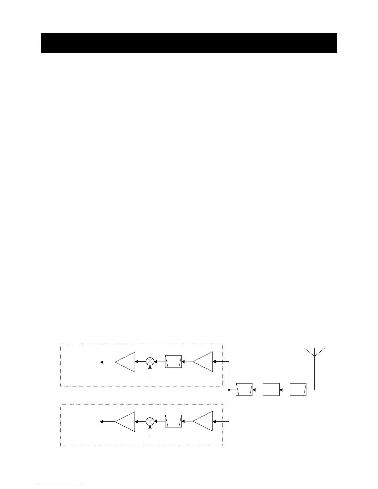
4-1 RECEIVER CIRCUITS
4-1-1 ANTENNA SWITCHING CIRCUIT (MAIN UNIT)
The antenna switching circuit functions as a low-pass filter
while receiving and as resonator circuit while transmitting.
The circuit does not allow transmit signals to enter the
receiver circuits.
Received signals enter the MAIN unit from the antenna con-
nector and pass through the low-pass filter (L1, L2, C1, C3,
C5). The signals are then applied to the RF circuit via the
antenna switching circuit (D1, L3, L4, C7–C9).
4-1-2 RF CIRCUIT (MAIN UNIT)
The RF circuit amplifies signals within the range of frequen-
cy coverage and filters out-of-band signals.
The signals from the antenna switching circuit pass through
the tunable bandpass filter (L11, C23–C25) which the object
signals are led to each RF amplifier of channel 70 circuit
(Q7) or other channels (except channel 70) circuit (Q1).
• CHANNEL 70 CIRCUIT
The amplified signals from the RF amplifier (Q7) are applied
to the 4-stage bandpass filter (L31–L34, C407, C408,
C410–C423) to suppress unwanted signals and improve the
selectivity. The signals are then applied to the 1st mixer cir-
cuit for channel 70.
•OTHER CHANNELS CIRCUIT
The amplified signals from the RF amplifier (Q1) are applied
to the 4-stage bandpass filter (L12–L15, C33, C34,
C36–C48) to suppress unwanted signals and improve the
selectivity. The signals are then applied to the 1st mixer cir-
cuit for other channels.
4-1-3 1ST MIXER AND 1ST IF CIRCUITS
(MAIN UNIT)
The 1st mixer circuit converts the received signal into a fixed
frequency of the 1st IF signal with a 1st LO (VCO output) fre-
quency. By changing the 1st LO frequency, only the desired
frequency will pass through a pair of crystal filters at the next
stage of the mixer.
•CHANNEL 70 CIRCUIT
The signals from the RF circuit are mixed with the 1st LO
signals at the 1st mixer circuit (D21, L48, L49) to produce a
21.7 MHz 1st IF signal.
The 1st IF signal is amplified at the 1st IF amplifiers (Q8,
Q9), and then passes through the pair of crystal bandpass
filters (FI4, FI5) to suppress out-of-band signals. The filtered
signal is then amplified at the 2nd IF amplifier (Q10), and is
then applied to the 2nd mixer circuit (IC6).
•OTHER CHANNELS CIRCUIT
The signals from the RF circuit are mixed with the 1st LO
signals at the 1st mixer circuit (D11, L18, L19) to produce a
31.05 MHz 1st IF signal.
The 1st IF signal is amplified at the 1st IF amplifiers (Q3,
Q4), and then passes through the crystal bandpass filter
(FI1) to suppress out-of-band signals. The filtered signal is
then amplified at the 2nd IF amplifier (Q2), and is then
applied to the 2nd mixer circuit (IC1).
RF
amp.
RF
amp.
RF
amp.
RF
amp.
LPF
IC5b
Ant sw.
IC5b
ANT
BPF
IC5b
BPF
IC5b
1st LO signal
to the 2nd mixer circuit
(IC1, pin 2)
to the 2nd mixer circuit
(IC6, pin 2)
For other channels
For channel 70 only
1st LO signal
BPF
IC5b
•1ST MIXER AND 1ST IF CIRCUITS

4 - 2
4-1-4 2ND IF AND DEMODULATOR CIRCUITS
(MAIN UNIT)
The 2nd mixer circuit converts the 1st IF signal into a 2nd IF
signal. A double superheterodyne system (which converts
receive signals twice) improves the image rejection ratio and
obtains stable receiver gain.
The FM IF IC (IC6 for channel 70, IC1 for other channels)
contains the 2nd local oscillator, 2nd mixer, limiter amplifier,
quadrature detector, and noise detector circuits, etc.
•CHANNEL 70 CIRCUIT
The 1st IF signal from the 2nd IF amplifier (Q10) is applied
to the 2nd mixer section of FM IF IC (IC6, pin 16), and is
mixed with a 21.25 MHz 2nd LO signal, which is generated
at the 2nd oscillator section in IC6 and X3, to produce a 450
kHz 2nd IF signal.
The 2nd IF signal from IC6 (pin 3) is passed through the
ceramic filter (FI6), which unwanted signals are suppressed,
and is then applied to the 2nd IF (limiter) amplifier in IC6 (pin
5). The signal is applied to the FM detector section in IC6 for
demodulating into AF signals.
The FM detector circuit employs a quadrature detection
method (linear phase detection), which uses a ceramic dis-
criminator (X2) for phase delay to obtain a non-adjusting cir-
cuit. The detected signal from IC6 (pin 9) is applied to the AF
circuit.
•OTHER CHANNELS CIRCUIT
The 1st IF signal from the 2nd IF amplifier (Q2) is applied to
the 2nd mixer section of FM IF IC (IC1, pin 16), and is mixed
with a 30.6 MHz 2nd LO signal, which is generated at the
PLL circuit using the reference frequency (15.3 MHz), to pro-
duce a 450 kHz 2nd IF signal.
The 2nd IF signal from IC1 (pin 3) is passed through the
ceramic filter (FI3), which unwanted signals are suppressed,
and is then applied to the 2nd IF (limiter) amplifier in IC1 (pin
5). The signal is applied to the FM detector section in IC1 for
demodulating into AF signals.
The FM detector circuit employs a quadrature detection
method (linear phase detection), which uses a ceramic dis-
criminator (X1) for phase delay to obtain a non-adjusting cir-
cuit. The detected signal from IC1 (pin 9) is applied to the AF
circuit.
2nd
Mixer
16
Limiter
amp.
2nd IF filter
450 kHz
X3
21.25 MHz
X2
(21.25 MHz)
IC6 TA31136FN
1st IF (21.7 MHz) from Q10
11109
16
IC11
IC3c,
IC3d
IC5a,
IC5b
"DEC2" signal
IC9
53
AF signal "DET"
8V
2
FI6
FM
detector
DSC
decoder
2nd
Mixer
16
Limiter
amp.
2nd IF filter
450 kHz
PLL IC
IC12
X4
15.3 MHz
X1
(30.6 MHz)
Q16
RSSI
IC1 TA31136FN
14 1st IF (31.05 MHz) from Q2
"NOISE" signal to the SQL amplifier (IC2, pin 1)
11109
17
IC11
IC3a
IC3b
"DEC1" signal
"WXDEC" signal
87 5 3
AF signal "DET"
8V
D/A convertor IC
(IC15, pin 23)
2
17 16
Active
filter
FI3
Noise
detector
FM
detector
2
DSC
decoder
•2ND IF AND DEMODULATOR CIRCUITS
(For CHANNEL 70 ONLY)
•2ND IF AND DEMODULATOR CIRCUITS
(For OTHER CHANNELS)

4 - 3
4-1-5 AF AMPLIFIER CIRCUIT (AF UNIT)
The AF amplifier circuit amplifies the demodulated signals to
drive a speaker. The AF circuit includes an AF mute circuit
for the squelch.
AF signals from the FM IF ICs (channel 70; IC6, pin 9, other
channels IC1, pin 9) are passed through the analog switch
(IC7, pins 10, 11) via the “DET”signal, and are applied to the
de-emphasis circuit (R31, C41). The de-emphasis circuit is
an integrated circuit with frequency characteristic of –6
dB/octave.
The signals pass through the bandpass filter (Q11, Q12),
and are then applied to the AF mute swtich (Q11). The sig-
nals passed through the [VOLUME] control (VR unit; R1),
and are then applied to the AF power amplifier (IC3, pin 1)
to obtain 5 W AF audio output power. The amplified AF sig-
nals drive the internal speaker as “SP+”signal directly or
external speaker as “AF”signal via the RL2.
4-1-6 SQUELCH CIRCUIT
(MAIN AND LOGIC UNITS)
A squelch circuit cuts out AF signals when no RF signals are
received. By detecting noise components in the AF signals,
the squelch circuit switches the AF mute switch.
A portion of the AF signals from the FM IF IC (IC1, pin 9) is
passed through C89, and is applied to the D/A converter
(IC15, pin 24) to control the amplitude. The signal is applied
to the FM IF IC’s active filter section (IC1, pin 8). The active
filter section amplifies and filters noise components. The fil-
tered signals are applied to the noise detector section and
output from pin 14 as the “SQL”signal. The “SQL”signal is
amplified at the DC amplifier (IC2) and applied to the main
CPU (LOGIC unit; IC1, pin 104) as the “SQL”signal. The
main CPU compares “SQL”voltage with “SQLV”voltage from
the SQL board, and outputs the “MICM”and “RMUTE”sig-
nals to toggle the AF mute switches (Q7, Q13).
4-2 TRANSMITTER CIRCUITS
4-2-1 MICROPHONE AMPLIFIER CIRCUIT
(AF UNIT)
The microphone amplifier circuit amplifies audio signals with
+6 dB/octave pre-emphasis from the microphone to a level
needed at the modulation circuit.
•USING HM-136
The AF signals from the microphone (ACC unit; HM-136)
are amplified at the microphone amplifier (IC6a) via the ana-
log switch (IC4, pins 11, 10) as “MIC”signal. A capacitor
(C77) and resistor (R73) are connected to the microphone
amplifier to obtain the pre-emphasis characteristics.
•USING HM-127
The AF signals from the microphone (ACC unit; HM-127)
are amplified at the microphone amplifier (IC6a) via the ana-
log switch (connecting option1 jack: IC16, pins 2, 3, 4; con-
necting option2 jack: IC16, pins 4, 9, 10) as “AF/MIC1”or
“AF/MIC2”signals. A capacitor (C77) and resistor (R73) are
connected to the microphone amplifier to obtain the pre-
emphasis characteristics.
The amplified signals are applied to the IDC amplifier (IC8a,
pin 2) via the analog switch (IC7, pins 2, 3, 9), and are then
passed through the splatter filter (IC8b) to suppress unwant-
ed 3 kHz or higher signals. The filtered signals are applied
to the modulation circuit.
4-2-2 MODULATION CIRCUIT (MAIN UNIT)
The modulation circuit modulates the VCO oscillating signal
(RF signal) using the microphone audio signals.
The audio signals from the splatter filter (IC8b) are passed
through the D/A converter IC (IC15, pins11, 12), and are then
applied to the modulation circuit. The applied signals change
the reactance of the varactor diode (D37), and modulate the
oscillated signal at the TX-VCO (Q18).
4-2-3 PRE-DRIVE AND YGR AMPLIFIERS CIRCUIT
(MAIN UNIT)
The drive amplifier circuit amplifies the VCO oscillating sig-
nal to a level needed at the power amplifier.
The output signal from VCO circuit is amplified at the buffer
amplifiers (Q19 and Q27), and is applied to the TX/RX
switch (D43). The transmit signal from the TX/RX switch is
amplified at the pre-drive (Q28) and YGR (Q30) amplifiers to
obtain an approximate 50 mW signal level. The amplified
signal is then applied to the RF power amplifier (IC13).
4-2-4 POWER AMPLIFIER CIRCUIT (MAIN UNIT)
The power amplifier circuit amplifies the driver signal to an
output power level.
IC13 is a power module which has amplification output
capabilities of about 35 W with 50 mW input. The output sig-
nal from IC13 (pin 1) is passed through the antenna switch-
ing circuit (D46) and is then applied to the antenna connec-
tor via the low-pass filter (L1, L2, L89, C1, C3, C5, C361,
C364).

4 - 4
4-2-5 APC CIRCUIT (MAIN UNIT)
The APC (Automatic Power Controller) circuit stabilizes the
TX output power.
The RF output signal from the power amplifier (IC13) is
detected at the power detector circuit (D47, D48) and is
applied to APC controller. The applied voltage compares to
“PCON”signal from the D/A converter IC (IC15, pin 14), and
then outputs the differential bias voltage for power amplifier
(IC13, pin 3). Thus the APC circuit maintains a constant out-
put power.
4-3 PLL CIRCUITS
4-3-1 GENERAL
The PLL circuit provides stable oscillation of the transmit fre-
quency and receive 1st LO frequency. The PLL circuit com-
pares the phase of divided VCO frequency with the refer-
ence frequency. The PLL output frequency is controlled by
the crystal oscillator and divided ratio of the programmable
divider.
IC12 is a dual PLL IC, which controls both TX and RX VCO
circuits, and contains a prescaler, programmable counter,
programmable divider, phase detector, charge pomp and
etc.
The PLL circuit, using a one chip PLL IC (IC12), directly gen-
erates the transmit frequency and receive 1st IF frequency
with VCOs. The PLL IC sets the divided ratio based on ser-
ial data from the main CPU, and compares the phases of
VCO signals with the reference oscillator frequency. The
PLL IC detects the out-of-step phase and outputs from pins
8 and 13 for TX and RX, respectively. The reference fre-
quency (15.3 MHz) is oscillated at the reference oscillator
(X4).
4-3-2 TX AND CHANNEL 70 (RX) LOOPS
The generated signal at the TX-VCO/CHANNEL 70-VCO
(Q18, D39, D40) enters the PLL IC (IC2, pin 2) and is divid-
ed at the programmable divider section and is then applied
to the phase detector section.
The phase detector compares the input signal with a refer-
ence frequency, and then outputs the out-of-phase signal
(pulse-type signal) from pin 8.
The pulse-type signal is converted into DC voltage (lock
voltage) at the loop filter (R217–R219, C247, C249, C278),
and is then applied to the varactor diodes (D39, D40) of the
TX-VCO to stabilize the oscillated frequency.
4-3-3 OTHER CHANNELS (RX) LOOP
The generated signal at the RX-VCO (Q12, D32, D33)
enters the PLL IC (IC2, pin 19) and is divided at the pro-
grammable divider section and is then applied to the phase
detector section.
The phase detector compares the input signal with a refer-
ence frequency, and then outputs the out-of-phase signal
(pulse-type signal) from pin 13.
The pulse-type signal is converted into DC voltage (lock
voltage) at the loop filter (R182, R213, R214, C225, C248),
and is then applied to the varactor diodes (D32, D33) of the
RX-VCO to stabilize the oscillated frequency. The lock volt-
age from the loop filter is amplified at the buffer amplifier
(Q23), and is then applied to the RF circuit.
D47 D48
L89
H/L
"TXDET" signal to the CPU
(LOGIC board; IC1, pin 106)
Q33
Pre
drive YGR
Q28 Q30
RF signal
from PLL to antenna
RF detector
circuit
APC control circuit
Power module
IC13
Q32
T8
"TMUTE" signal from the CPU
(LOGIC board; IC1, pin 93)
IC14 "PCON" signal from the D/A
convertor (IC15, pin 14)
•APC CIRCUIT

4 - 5
4-3-4 VCO CIRCUIT (MAIN UNIT)
•TX-VCO/CHANNEL 70-VCO (RX) CIRCUITS
The VCO outputs from TX-VCO/CHANNEL 70-VCO (Q18)
are amplified at the buffer amplifiers (Q19 and Q27), and are
applied to the TX/RX switch circuit (D42, D43). The receiver
LO signal is applied to the 1st mixer circuit for CHANNEL 70
(D21, L48, L49) passing through a low-pass filter (L51, L52,
C150–C152), and the transmitter signal is applied to the pre-
drive amplifier (Q28). A portion of the VCO output signal is
re-applied to the PLL IC (IC2, pin 2) via the buffer amplifier
(Q15).
•OTHER CHANNELS-VCO (RX) CIRCUITS
The VCO outputs from OTHER CHANNELS-VCO (Q12) are
amplified at the buffer amplifiers (Q13 and Q23). The receiv-
er LO signal is applied to the 1st mixer circuit for OTHER
CHANNELS (D11, L18, L19) passing through a low-pass fil-
ter (L21, L22, C52–C54). A portion of the VCO output signal
is re-applied to the PLL IC (IC2, pin 2 or pin 19) via the buffer
amplifier (Q19).
4-4 DSC CIRCUITS
4-4-1 DSC MODULATION CIRCUIT
(LOGIC, AF AND MAIN UNITS)
The ATIS signal from the CPU (LOGIC unit; IC1, pin 117) is
applied to the buffer amplifier (AF unit; Q18) as “DSC”sig-
nal. The signal passes through the analog switch (AF unit;
IC7, pin 1), and then applied to IDC amplifier (AF unit; IC8a).
Then, the amplified signal is applied to the transmitter cir-
cuit.
The signalis passed through the splatter filter (AF unit; IC8b)
to suppress unwanted 3 kHz or higher signals. The filtered
signals are then applied to the TX modulation circuit via the
D/A converter IC (MAIN unit; IC15, pins 11, 12) as a DSC
modulation signal “MOD”.
4-5 LOGIC CIRCUITS
4-5-1 MAIN UNIT
•CPU
IC1 is a 8 bit single chip micro-computer, which contains
LCD driver, serial I/O, timer, A/D converter, programmable
I/O, ROM and RAM.
•SYSTEM CLOCK CIRCUIT
X1 is a crystal oscillator, which oscillates 9.8304 MHz sys-
tem clock for the main CPU (IC1).
•RESET CIRCUIT
IC2 is a reset IC, which outputs a reset signal (“LOW”pulse)
to main CPU (IC1, pin 79) when turning transceiver power
ON.
Loop
filter
X2
15.3 MHz
Shift register/
data latch
IC12 (PLL IC)
Prescaler
Phase
detector
Programmable
counter
Programmable
divider
3
4
5
2
8
2
PSTB
PCK
PDATA
30.6 MHz signal
to the FM IF IC
(IC1, pin 2)
Buffer
Buffer
Buffer
Q27
Q15
Q19
to transmitter circuit
to 1st mixer circuit
D42
D43
17
Q16
16
Q18, D39, D40
VCO
•PLL CIRCUIT
Buff.
amp.
IC8
"DSC" signal from the CPU
(LOGIC board; IC1, pin 117)
Q19
analog
switch
IDC
amp.
IC8a
LPF
IC5b
D/A
convertor
IC15
to VCO circuit
•DSC CIRCUIT

4 - 6
4-6 POWER SUPPLY CIRCUITS
4-6-1 VOLTAGE LINE (MAIN UNIT)
4-7 PORT ALLOCATIONS
4-7-1 EXPANDER IC (AF unit; IC18)
4-7-2 EXPANDER IC (AF unit; IC17)
LINE
13.8
HV
HVS
VCC
8V
5V
T8
R8
DESCRIPTION
The 13.8 V from the connected DC power sup-
ply.
Same voltage as the HV line which is passed
through the [PWR] switch (LOGIC unit; S1).
Same voltage as the HVS line which is passed
through the power controller (AF unit; RL1).
Same voltage as the 13.8 V line, and is applied
to the AF power amplifiers (AF unit; IC3, IC10),
LOGIC unit, etc.
Common 8 V converted from the VCC line at the
+8V regulator circuit (AF unit; IC1). The output
voltage is applied to the T8 controller (MAIN unit;
Q36, Q36), +5 regulator (AF unit; IC2), R8 regu-
lator (AF unit; Q1, Q2), etc.
Common 5 V converted from the 8V line at the
+5 regulator circuit (AF unit; IC2). The output
voltage is applied to the buffer amplifiers (AF
unit; IC19, Q14), expander ICs (AF unit; IC17,
IC18), etc.
Transmit 8 V controlled by the T8 control circuit
(MAIN unit; Q35, Q36) using the “SEND” signal
from main CPU. The output voltage is applied to
the pre-dirve (MAIN unit; Q28), YGR amplifier
(MAIN unit; Q30), APC controller (MAIN unit;
IC14), etc.
Receive 8 V controlled by the R8 control circuit
(AF unit; Q1, Q2) using the RCV signal from
main CPU. The controlled voltage is applied to
the bandpass filter (AF unit; Q11, Q12), buffer
and IF amplifiers (AF unit; Q2 and Q23), etc.
4
5
6
7
11
12
13
14
MICS2
MICS1
SPS2
SPS1
SP
BPLVL
RCV
HLC
Outputs HM-134/2 control signal.
High : While transmitting via the
HM-134/2.
Outputs HM-134/1 control signal.
High : While transmitting via the
HM-134/1.
Outputs HM-134/2 control signal.
High : While receiving via the
HM-134/2.
Outputs HM-134/1 control signal.
High : While receiving via the
HM-134/1.
Outputs the internal speaker (FRONT
unit; SP1) control signal.
High : The speaker is activating.
Outputs beep audio level control sig-
nal.
Low : Beep audio level is maximum.
Outputs the R8 regulator (AF unit; Q1,
Q2) control signal.
High : While receiving.
Outputs the Hailer speaker TX/RX
select signal.
High : While transmitting via the
Hailer speaker.
Pin Port Description
number name
4
5
6
7
11
12
13
14
STRU
AFSUB
INCMH
INCHM
MIC/DSC
HAILIN
FOGC
HAILOUT
Outputs scrambler unit bypass control
signal.
High : Bypassing the scrambler unit.
Outputs sound signals to the HM-134.
High : Sounding from HM-134.
Outputs voice signals from IC-M601 to
HM-134 using intercom function.
High : While receiving.
Outputs voice signals from HM-134 to
IC-M601 using intercom function.
High : While transmitting.
Outputs MIC/DSC modulation circuit
control signal.
High : While the DSC signal is mod-
ulated.
Outputs the microphone select signal.
High : While using the hailer speak-
er.
Outputs fog horn control signal.
High : Fog horn is ON.
Outputs the microphone select signal.
High : While using the HM-137.
Pin Port Description
number name

4 - 7
4-7-3 CPU (LOGIC BOARD; IC1)
Input port for the indide temperature
detecting signal.
Input ports for the dial data signals.
Input port for the HM-137’s PTT button
detecting signal.
Low : While PTT button is pushed.
Input port for the microphone hanger
detecting signal.
Low : The microphone on hook.
Outputs ATIS/DSC encode signals.
Outputs the voice scramber unit
(UT-112) control signal.
Outputs a strobe signal to the voice
scrambler unit (UT-112).
Outputs a strobe signal to the PLL IC
(MAIN unit; IC12, pin 3).
Outputs a strobe signal to the D/A
convertor IC (MAIN unit; IC15, pin 6).
I/O port for the communicating singal
from the microphone (HM-134/2) to
the transceiver.
I/O port for the communicating singal
from the transceiver to the micro-
phone (HM-134/2).
TEMP
DIAL1–
DIAL4
PTT
HANG
DSC
SCON
OPSTB
DASTB
PSTB
DATAH2M
DATAMH2
107
111–114
115
116
117
120
121
124
125
126
127
7
25
28
34
38
39
58
59
63
64
66
69
70
71
74
91
93
94
95
103
104
105
106
UNLK
EDATA
ECK
DEC3
.
DEC1
BEEP
DATAMC
DATACM
DATAMH1
DATAH1M
DATANM
DATAMN
PDATA
PCK
OPTIN
RMUTE
TMUTE
SEND
H/L
WXDEC
SQL
LBAT
TXDET
Input port for PLL unlock signal from
the PLL IC (MAIN unit; IC12, pin 7).
High : While PLL is unlocked.
I/O port for the data signals to the
EEPROM (IC4, pin 5).
Outputs a clock signal to the EEP-
ROM (IC4, pin 6).
Input port for the decode signal for
channel 70 receiver.
Input port for the ATIS/DSC decode
signals.
Outputs beep audio signals.
I/O port for the cloning data from the
transceiver.
I/O port for the cloning data to the
transceiver.
I/O port for the communicating signal
from the transceiver to the micro-
phone (HM-134/1).
I/O port for the communicating signal
from the microphone (HM-134/1) to
the transceiver.
I/O port for the GGA signals
I/O port for the NMEA data.
Outputs a data signal to the PLL IC
(MAIN unit; IC12, pin 5).
Outputs a clock signal to the PLL IC
(MAIN unit; IC12, pin 4).
Outputs the voice scrambler unit
(UT-112) detecting signal.
Low : While UT-112 is connecting.
Outputs RX muting signal.
High : While RX signal is muting.
Outputs transmit mute signal.
High : While TX muting.
Outputs T8 regulator control signal.
High: While transmitting.
Output port for RF output power (High
or Low) select signal.
Low : While Low power is selected.
Input port for the weather alert signal.
Input port for the FM IF IC (MAIN unit;
IC1, pin 14)’s noise amplifier detecting
signal.
Input port for the low-battery detecting
signal. Low battery indicator appears
when the battery becomes less than
2.58 V.
Input port for transmit detecting signal.
Pin Port Description
number name
Pin Port Description
number name

5 - 1
SECTION 5 ADJUSTMENT PROCEDURES
5-1 PREPARATION
■REQUIRED TEST EQUIPMENT
■CONNECTION
EQUIPMENT
DC power supply
External speaker
Tracking generator
GRADE AND RANGE
Output voltage : 13.8 V DC
Current capacity : 10 A or more
Input impedance : 4 Ω
Capacity : 5 W or more
Frequency range : 100–300 MHz
Output level : 0.1 µV–32 mV
(–127 dBm to –17 dBm)
EQUIPMENT
Standard signal
generator (SSG)
DC voltmeter
Distortion meter
GRADE AND RANGE
Frequency range : 0.1–300 MHz
Output level : 0.1 µV–32 mV
(–127 to –17 dBm)
Input impedance : 50 kΩ/V DC or better
Frequency range : 1 kHz ±10 %
Measuring range : 1–100 %
IC-M601 rear panel
NOTE: EXTERNAL SPEAKER JACK PIN CONNECTION
Power supply
13.8 V / 10 A or more
Tracking generator
Standard signal generator
0.1 300 MHz
127 dBm to 17 dBm
(0.1 V to 32 mV)
4 load Distortion meter
CAUTION!
DO NOT transmit while an
SSG is connected to the
antenna connector.
to the antenna
connector
to external speaker jack
NMEAOUT (+)
NMEAIN ( )
SP ( )
CLONE GND SP (+)
NMEAIN (+)
NMEAOUT ( )
ICF3
NC

5 - 2
Lock voltage
adjustment for TX
L73
Lock voltage
check point for RX
CP1 Lock voltage
check point for TX
CP2
L62
Lock voltage
adjustment for RX
5-2 PLL ADJUSTMENTS
LOCK
VOLTAGE
ADJUSTMENT
ADJUSTMENT ADJUSTMENT CONDITION MEASUREMENT VALUE POINT
UNIT LOCATION UNIT ADJUST
1
2
3
•Operating channel : ch P2
•Receiving
•Operating channel : ch P2
•Output power : Low
•Transmitting
•Operating channel : ch 70
•Receiving
MAIN Connect a digital
multi-meter or oscil-
loscope to check
point CP1.
Connect a digital
multi-meter or oscil-
loscope to check
point CP2.
3.8 V –4.0 V
3.1 V –3.3 V
2.7–3.7 V
MAIN L62
L73
Verify
•MAIN UNIT TOP VIEW

5 - 3
*This output level of a standard signal generator (SSG) is indicated as SSG’s open circuit.
5-3 RECEIVER ADJUSTMENTS
SENSITIVITY
(Except
channel 70)
(Channel 70)
ADJUSTMENT
ADJUSTMENT ADJUSTMENT CONDITION MEASUREMENT VALUE POINT
UNIT LOCATION UNIT ADJUST
1
2
•Operating channel : ch 16
•Connect a tracking generator’s
output to the antenna connector
and set as:
Level : 7.1 mV*
(–30 dBm)
•Operating channel : ch 16
•Connect an SSG to the antenna
connector and set as:
Frequency : 156.800 MHz
Level : 10 µV*
(–97 dBm)
Modulation : 1 kHz
Deviation : ±3.5 kHz
•Set the internal speaker OFF in
the SET mode, and connect a
distortion meter with a 4 Ωload to
[EXT SP] receptacle.
•Receiving
MAIN
MAIN
Connect a tracking
generator’s input to
the MAIN unit; J3.
Connect a DC volt-
meter to check point
CP3.
Set the flat wave
form as shown below.
Maximum voltage
MAIN
MAIN
L11
L12
L13
L14
L15
L31
L32
L33
L34
155 MHz 165 MHz
Set to flat wave form

5 - 4
L11
L12
L13
L14
L15
J9
RX sensitivity adjustment
for other channels
RX sensitivity check point
L31
L34
L33
L32 RX sensitivity adjustment
for channel 70
•MAIN UNIT TOP VIEW
Table of contents
Other Icom Transceiver manuals

Icom
Icom IC-M1EURO V User manual

Icom
Icom IC-M120 User manual

Icom
Icom IC-2100H User manual

Icom
Icom IC-229A User manual

Icom
Icom IC-M127EURO User manual

Icom
Icom IC-F4029SDR User manual

Icom
Icom IC-F5330D User manual

Icom
Icom IC-M3EURO User manual

Icom
Icom IC-290A User manual

Icom
Icom IC-F41GS Building instructions