Icom ID-800H User manual

GUIDE FOR CD
1) COMPOSION
1
ID_800H ID800.pdf
FYC A3format.pdf
A4format.pdf
Instruction.pdf
Unitparts.pdf
Installer ar505eng.exe
W_README.txt
2) DESCRIPTION
A3format.pdf
Consists of A3 format pages (Board layouts, Mechanical parts and disassembly, and etc.). This file is used for printing out A3
format pages.
ID800.pdf
The service manual for ID-800H including all service information in this CD. This file is mainly used for viewing on the computer
display and checking page order to make printed service manual. Or when you want to find a component, you can find very fast
using “FIND” function (except Board Layouts).
A4format.pdf
Consists of A4 format pages (Circuit description, Adjustment procedures, Parts list, and etc.). This file is used for printing out A4
format pages.

2
=========================================================================================
Icom, Icom Inc. and Icom logo are registered trademarks of Icom Incorporated (Japan) in the United states, the
United Kingdom, Germany, France, Spain, Russia and/or other countries.
Acrobat Reader Copyright © 1987-2002 Adobe Systems Incorporated. All rights reserved.
Adobe, the Adobe logo, Acrobat, and the Acrobat logo are trademarks of Adobe Systems Incorporated.
Microsoft and Windows are registered trademarks of Microsoft Corporation in the U.S.A. and other countries.
Copyright 2005 Icom Inc.
=========================================================================================
ar505eng.exe
ar505eng.exe is an installation program of Adobe®Reader 5.0 (English version) for Microsoft®Windows®95/98/
Me/NT/2000/XP users.
W_README.txt
W_README.txt is a readme text about this service manual for Windows®user that not installed Adobe®Reader
yet.
Instruction.pdf
The instruction manual for ID-800H. The contents of this file is exactly same as supplied instruction manual with product and
consists of all A4 format pages. If you have A4 format printer, you can print and make brand new instruction manual any time you
want. This file is also very helpful when you want to change or set product setting condition for adjustment or else.
Unitparts.pdf
Uitparts.pdf is assemble unit information for ID-800H. This information for authorized dis-tributor/dealer only. Because we (ICOM
INC.) don’t sell assemble unit to general.

SERVICE
MANUAL
VHF/UHF DIGITAL TRANSCEIVER
S-14121HZ-C1
May. 2005

INTRODUCTION
This service manual describes the latest service information
for the ID-800H VHF/UHF DIGITAL TRANSCEIVER at the
time of publication.
DANGER
NEVER connect the transceiver to an AC outlet or to a DC
power supply that uses more than 16 V. This will ruin the
transceiver.
DO NOT expose the transceiver to rain, snow or any liquids.
DO NOT reverse the polarities of the power supply when
connecting the transceiver.
DO NOT apply an RF signal of more than 20 dBm (100
mW) to the antenna connector. This could damage the
transceiver’s front end.
ORDERING PARTS
Be sure to include the following four points when ordering
replacement parts:
1. 10-digit order numbers
2. Component part number and name
3. Equipment model name and unit name
4. Quantity required
<SAMPLE ORDER>
1140005990 S.IC MB15A02PFV ID-800H MAIN UNIT 5 pieces
8810009610 Screw FH M2.6×6 ZK ID-800H Bottom cover 10 pieces
Addresses are provided on the inside back cover for your
convenience.
REPAIR NOTES
1. Make sure a problem is internal before disassembling
the transceiver.
2. DO NOT open the transceiver until the transceiver is
disconnected from its power source.
3. DO NOT force any of the variable components. Turn
them slowly and smoothly.
4. DO NOT short any circuits or electronic parts. An
insulated tuning tool MUST be used for all adjustments.
5. DO NOT keep power ON for a long time when the
transceiver is defective.
6. DO NOT transmit power into a signal generator or a
sweep generator.
7. ALWAYS connect a 50 dB to 60 dB attenuator between
the transceiver and a deviation meter or spectrum
analyzer when using such test equipment.
8. READ the instructions of test equipment thoroughly
before connecting equipment to the transceiver.
To upgrade quality, any electrical or mechanical parts and
internal circuits are subject to change without notice or
obligation.
Icom, Icom Inc. and
logo are registered trademarks of Icom Incorporated (Japan) in the United States, the United
Kingdom, Germany, France, Spain, Russia and/or other countries.
MODEL VERSION SYMBOL
ID-800H U.S.A. USA
Export EXP

TABLE OF CONTENTS
SECTION 1 SPECIFICATIONS
SECTION 2 INSIDE VIEWS
SECTION 3 DISASSEMBLY INSTRUCTIONS
SECTION 4 CIRCUIT DESCRIPTION
4 - 1 RECEIVER CIRCUITS . . . . . . . . . . . . . . . . . . . . . . . . . . . . . . . . . . . . . . . . . . . . . . . . . . . . . . . . . . . . . . .4 - 1
4 - 2 TRANSMITTER CIRCUITS . . . . . . . . . . . . . . . . . . . . . . . . . . . . . . . . . . . . . . . . . . . . . . . . . . . . . . . . . . . .4 - 4
4 - 3 PLL CIRCUITS . . . . . . . . . . . . . . . . . . . . . . . . . . . . . . . . . . . . . . . . . . . . . . . . . . . . . . . . . . . . . . . . . . . . .4 - 6
4 - 4 POWER SUPPLY CIRCUITS. . . . . . . . . . . . . . . . . . . . . . . . . . . . . . . . . . . . . . . . . . . . . . . . . . . . . . . . . . .4 - 8
4 - 5 OTHER CIRCUITS . . . . . . . . . . . . . . . . . . . . . . . . . . . . . . . . . . . . . . . . . . . . . . . . . . . . . . . . . . . . . . . . . .4 - 9
4 - 6 PORT ALLOCATIONS . . . . . . . . . . . . . . . . . . . . . . . . . . . . . . . . . . . . . . . . . . . . . . . . . . . . . . . . . . . . . . .4 - 10
SECTION 5 ADJUSTMENT PROCEDURES
5 - 1 PREPARATION . . . . . . . . . . . . . . . . . . . . . . . . . . . . . . . . . . . . . . . . . . . . . . . . . . . . . . . . . . . . . . . . . . . . .5 - 1
5 - 2 CODEC ADJUSTMENT. . . . . . . . . . . . . . . . . . . . . . . . . . . . . . . . . . . . . . . . . . . . . . . . . . . . . . . . . . . . . . .5 - 3
5 - 3 SOFTWARE ADJUSTMENT . . . . . . . . . . . . . . . . . . . . . . . . . . . . . . . . . . . . . . . . . . . . . . . . . . . . . . . . . . .5 - 4
SECTION 6 PARTS LIST
SECTION 7 MECHANICAL PARTS AND DISASSEMBLY
SECTION 8 SEMI-CONDUCTOR INFORMATION
SECTION 9 BOARD LAYOUTS
9 - 1 CONTROL UNIT . . . . . . . . . . . . . . . . . . . . . . . . . . . . . . . . . . . . . . . . . . . . . . . . . . . . . . . . . . . . . . . . . . . .9 - 1
9 - 2 MAIN UNIT . . . . . . . . . . . . . . . . . . . . . . . . . . . . . . . . . . . . . . . . . . . . . . . . . . . . . . . . . . . . . . . . . . . . . . . .9 - 3
9 - 3 VCO BOARD . . . . . . . . . . . . . . . . . . . . . . . . . . . . . . . . . . . . . . . . . . . . . . . . . . . . . . . . . . . . . . . . . . . . . . .9 - 5
9 - 4 CODEC BOARD . . . . . . . . . . . . . . . . . . . . . . . . . . . . . . . . . . . . . . . . . . . . . . . . . . . . . . . . . . . . . . . . . . . .9 - 5
SECTION 10 BLOCK DIAGRAM
SECTION 11 VOLTAGE DIAGRAMS
11 - 1 MAIN UNIT . . . . . . . . . . . . . . . . . . . . . . . . . . . . . . . . . . . . . . . . . . . . . . . . . . . . . . . . . . . . . . . . . . . . . . .11 - 1
11 - 2 CODEC BOARD . . . . . . . . . . . . . . . . . . . . . . . . . . . . . . . . . . . . . . . . . . . . . . . . . . . . . . . . . . . . . . . . . . .11 - 5
11 - 3 CONTROL UNIT . . . . . . . . . . . . . . . . . . . . . . . . . . . . . . . . . . . . . . . . . . . . . . . . . . . . . . . . . . . . . . . . . . .11 - 6

SECTION 1 SPECIFICATIONS
1 - 1
MGENERAL
• Frequency range :
• Type of emission : FM, GMSK, AM (118.0–135.995 MHz range and Rx only.)
• Digital Transmission speed : 4.8 kbps
• CODEC : AMBE 2.4 kbps
• Number of memory channel : 512 (including 10 scan edges and 2 calls)
• Usable temperature range : –10˚C to +60˚C; +14˚F to +140˚F
• Frequency resolution : 5, 10, 12.5, 15, 20, 25, 30, 50, 100, 200 kHz
• Frequency stability : ±2.5 ppm (–10˚C to +60˚C; +14˚F to +140˚F)
• Power supply requirement : 13.8 V DC ±15% (negative ground)
• Current drain (at 13.8 V DC) :
• Antenna connector : SO-239 (50 Ω)
• Dimensions (proj. not included) : 141(W)×40(H)×185.4(D) mm; 59⁄16(W)×19⁄16(H)×75⁄16(D) inch
• Weight (approx.) : 1.2 kg; 2 lb 10 oz
MTRANSMITTER
• Output power (at 13.8 V DC; typ.) : VHF 55 W /15 W/5 W (selectable)
UHF 50 W/15 W/5 W (selectable)
• Modulation system : FM Variable reactance frequency modulation
DV GMSK
• Maximum frequency deviation : ±5.0 kHz
• Spurious emissions : Less than –60 dB
• Microphone connector : 8-pin modular jack (600 Ω)
MRECEIVER
• Receive system : Double-conversion superheterodyne
• Intermediate frequencies : 1st IF 46.05 MHz, 2nd IF 450 kHz
• Sensitivity : FM Less than 0.18 µV (–122 dBm) at 12 dB SINAD
DV Less than 0.35 µV (–116 dBm) at BER 1×10⁻²
• Squelch sensitivity : Less than 0.13 µV (–125 dBm) at threshold
• Selectivity : Wide More than 12 kHz/6 dB, Less than 30 kHz/60 dB
Narrow More than 6 kHz/6 dB, Less than 20 kHz/60 dB
• Spurious and image rejection : More than 60 dB
• AF output power (at 13.8 V DC) : More than 2.0 W at 10% distortion with an 8 Ω load
• External speaker connector : 3-conductor 3.5(d) mm (1⁄8")/8 Ω
All stated specifications are subject to change without notice or obligation.
VERSION RX (MHz) TX (MHz)
[USA]
118.000–173.995*1, 230.000–549.995*3
810.000–824.000*4, 849.000–869.000*4
894.000–999.990*4
144.000–148.000, 440.000–450.000
[EXP] 118.000–173.995*1, 230.000–549.995*2
810.000–999.990*4144.000–148.000, 430.000–440.000
*1Guaranteed 144.000–148.000 MHz, *2Guaranteed 430.000–440.000 MHz
*3Guaranteed 440.000–450.000 MHz, *4Not guaranteed
VHF UHF
TX
High 12 A (at 55 W) 12.5 A (at 50 W)
Middle 7.5 A (at 15 W) 7.5 A (at 15 W)
Low 5.5 A (at 5 W) 5.0 A (at 5 W)
RX Standby 0.9 A
Max. audio 1.1 A

SECTION 2 INSIDE VIEWS
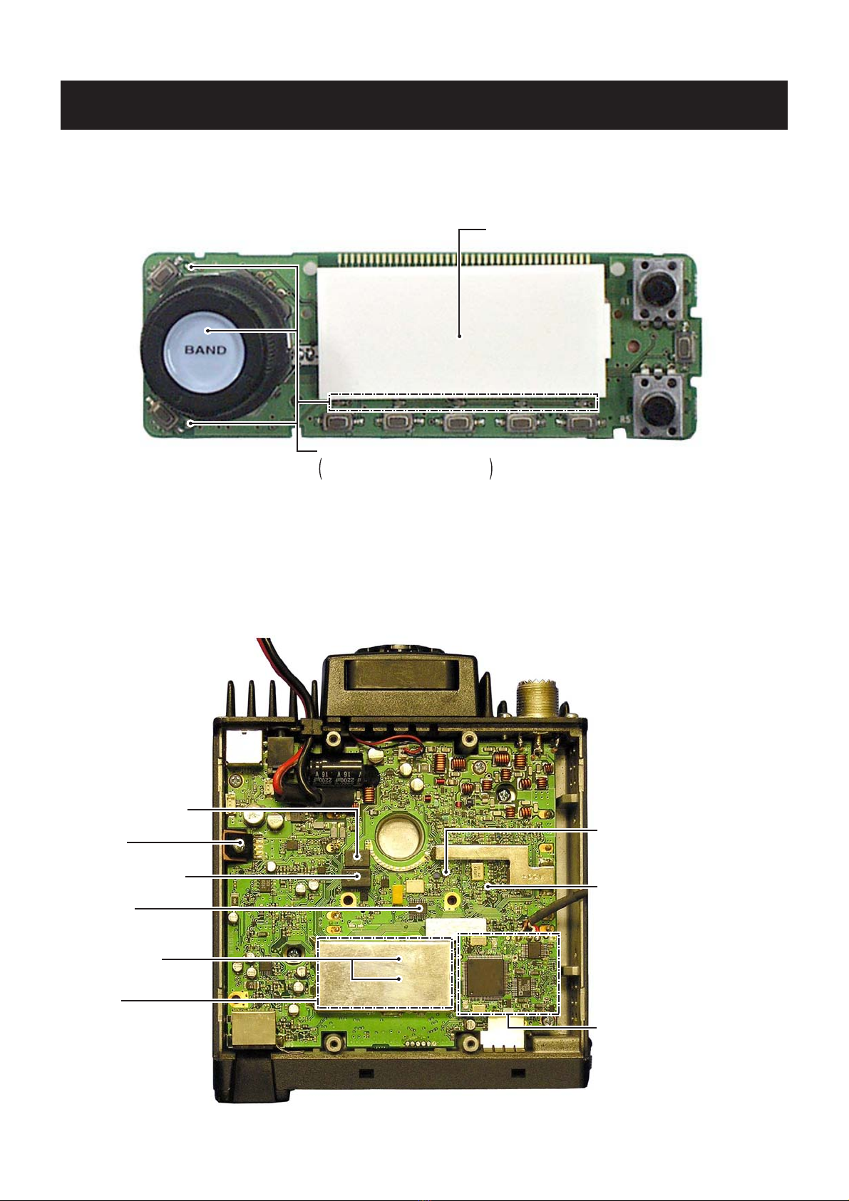
• CONTROL UNIT (TOP VIEW)
• MAIN UNIT (TOP VIEW)
2 - 1
LCD back light
(DS22: CV1074)
Key back light
DS13-DS18,DS20: SML512MW
DS21: SML-020MYT
LCD backlight
(DS22: CV1074)
Key backlights
DS13-DS18, DS20: SML512MW
DS21: SML-020MYT
VCO board
AF amplifier
(IC510: LA4425A)
1st mixcer [VHF band]
(Q32: 3SK299)
1st mixcer [400M,800MHz band]
(IC12: µPC2757TB)
D/A converter
(IC11: M62352GP)
VCO board
PLL ICs (main unit)
(IC1, IC2: MB15A02PFV-1)
AF amplifier
(IC510: LA4425A)
1st mixer [VHF band]
(Q32: 3SK299)
1st mixer
[400M band], [800M band]
(IC12: µPC2757TB)
D/A converter
(IC11: M62352GP)
Ceramic bandpass filter
(FI2: CFWM450E)
Ceramic bandpass filter
(FI1: CFWS450HT)
CODEC board

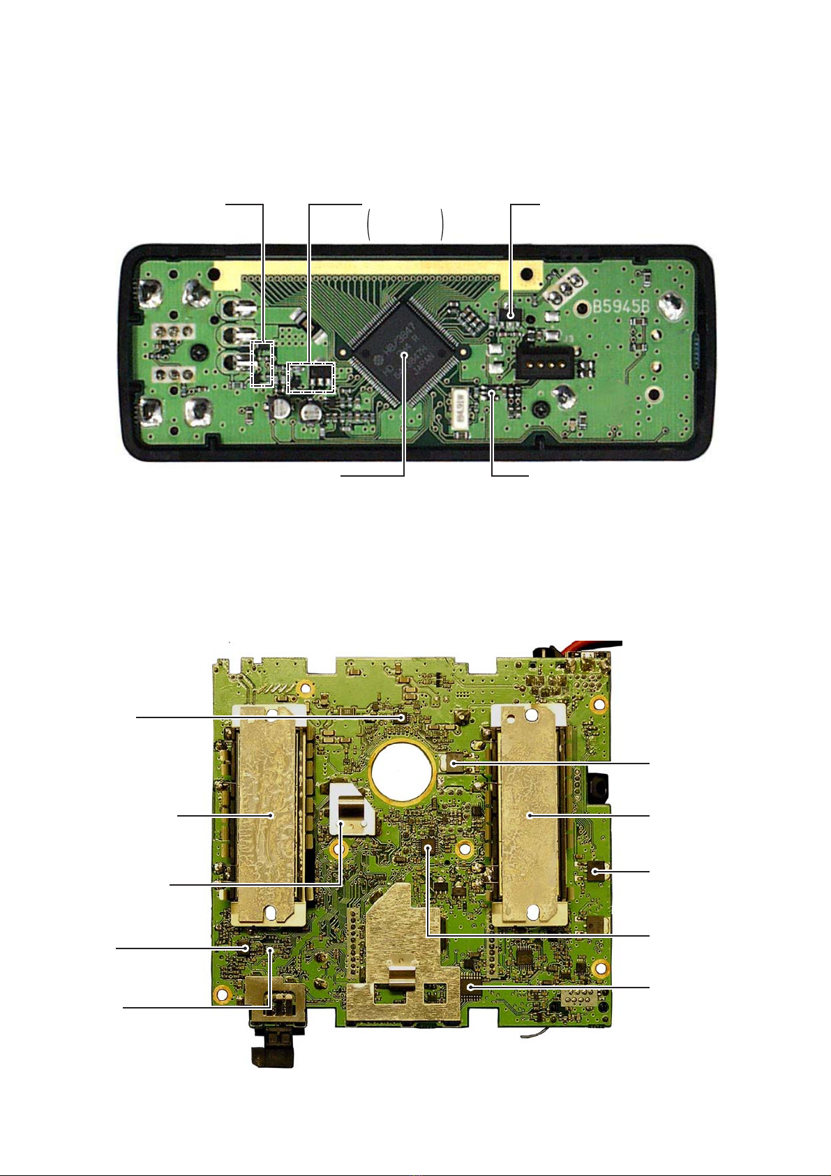
• CONTROL UNIT (BOTTOM VIEW)
• MAIN UNIT (BOTTOM VIEW)
Color controller
(Q6,Q7: 2SC4116)
Control unit CPU
(IC6: HD6433842RB36H) Reset IC
(IC2: S-80945CLMC-G7F)
+8V regurator
Q1: 2SC4116
Q3: 2SA1734
D5: MA8068
Color controller
(Q6, Q7: 2SC4116)
Control unit CPU
(IC6: HD6433842RC37H) Reset IC
(IC2: S-80945CLMC-G7F)
+5V regulator
(IC5: TA78L05F)
+8V regulator
Q1: 2SC4116
Q3: 2SA1734
D5: MA8068
+8V regurator
(IC504: TA7808F)
+5V regurator
(IC503: TA7805F)
D/A converter
(IC4: M62363FP-650C)
IF IC
(IC8: TA31136FN)
APC controller
(IC15: NJM3404AV)
1st mixer [UHF band]
(Q35: 3SK299)
PA module [UHF band]
(IC14: S-AU82L) PA module [VHF band]
(IC13: S-AV32)
+8V regulator
(IC504: TA7808F)
+5V regulator
(IC503: TA7805F)
D/A converter
(IC4: M62364FP)
FM IF IC
(IC8: TA31136FN)
APC amplifier
(IC15: NJM3404AV)
1st mixer [UHF band]
(Q35: 3SK299)
PA module [UHF band]
(IC14: S-AU82L) PA module [VHF band]
(IC13: S-AV32)
PA module [UHF band]
(IC14: S-AU82L)
EEPROM
(IC501: HN58X24128FPI)
MAIN CPU*
(IC505: HD64F2144AFA20)
* Located top side of the point.
2 - 2

SECTION 3 DISASSEMBLY INSTRUCTIONS
• REMOVING THE MAIN UNIT AND CODEC BOARD
1Unscrew 4 screws A, and remove the cover.
2
Disconnect the cable Bfrom J505, and remove the speaker.
3Remove 2 cube shaped rubbers C.
Continue to right above.
3 - 1
4Disconnect the cable Dfrom J508.
5Disconnect the cable Efrom J1.
6Unscrew 3 screws F, and remove the shield cover G.
7Remove the CODEC board from J507.
8Unsolder 3 points H.
J505J505
B
C
A
A
J1
J508
F
G
E
D
VCO
H
CODEC board
J507
9Unscrew 8 screws I, and remove the MAIN unit.
I
MAIN UNIT

3 - 2
• REMOVING THE CONTROL UNIT
1Remove 2 knobs A.3Unscrew 2 screws C, and remove the LCD plate.
4Remove the CONTROL unit.
2Unscrew 2 screws B, and remove the cover.
A
B
Continue to right above.
C
CONTROL UNIT

4 - 1
SECTION 4 CIRCUIT DESCRIPTION
4-1 RECEIVER CIRCUITS
4-1-1 TRIPLEXER CIRCUIT (MAIN UNIT)
The transceiver has a triplexer (low-pass and high-pass
filters) on the first stage from the antenna connector
(CHASSIS; J2) to separate the signals into VHF, UHF and
800 MHz band signals. The 2 of low-pass filters (L51, L52,
L56, C295, C299 and L45, L46, L49, C282, C285, C289)
are for VHF band signals, the low-pass (L51, L52, L56,
C295, C299) and high-pass (L47, L50, C284, C288, C292,
C586) filters are for UHF band signals and high-pass filter
(L55, L58, C298, C302, C304) is for 800 MHz band signals.
The separated signals are applied to each antenna switching
circuits .
4-1-2 ANTENNA SWITCHING CIRCUITS (MAIN UNIT)
The antenna switching circuit (VHF: D50, UHF: D51)
functions as a low-pass filter while receiving. However,
its impedance becomes very high while transmitting.
Thus transmit signals are blocked from entering the
receiver circuits. The antenna switching circuit employs a
1⁄4λtype diode switching system.
800 MHz band signals pass through the antenna switch
(D44).
The passed signals are then applied to the each attenuator
circuits.
4-1-3 ATTENUATOR CIRCUITS (MAIN UNIT)
The attenuator circuit attenuates the signal strength to a
maximum of 10 dB to protect the RF amplifier from distor-
tion when excessively strong signals are received.
The RF signals from the antenna switching circuits pass
through the each attenuator circuit (for VHF band is D49, for
UHF band is D46 and D48, for 800 MHz band is D39).
The D/A converter outputs “ATT” signal (IC11, pin 6), and is
then applied to the attenuator controller (Q44). The circuit
output attenuator control signals to each attenuator circuits.
The attenuated signals are applied to the each RF circuits.
4-1-4 RF CIRCUITS (MAIN UNIT)
The RF circuit amplifies signals within the range of frequen-
cy coverage and filters out-of-band signals.
• VHF BAND RF CIRCUIT (118–174 MHz)
The RF signals from the attenuator circuit pass through the
tunable bandpass filter (D41, L40, L44, C273, C280). The
filtered signals are amplified at the RF amplifier (Q38) and
are then applied to the another 3-stage tunable bandpass
filter (D22, D23, D29, L28, C171, C174, C176, C177, C181,
C185, C191, C198, C201, C204, C208) to suppress unwant-
ed signals and improve the selectivity. The filtered signals
are applied to the VHF 1st mixer circuit (Q32).
• UHF BAND RF CIRCUIT
(EXP: 430–440 MHz, USA: 440–450 MHz)
The RF signals from the attenuator circuit are applied to the
RX switch (D42). The switched signals are amplified at the
RF amplifier (Q39) and are then applied to the bandpass
filter (FI4) to suppress unwanted signals. The filtered signals
are applied to the UHF 1st mixer circuit (Q35).
LPF
VHF band (118−174 MHz)
to the 2nd IF circuit
1st mixer (Q32)
Q38
Q39
D9
D8
D10 D17
D18
Q36
Q37 Q41
Q40
D44
D43
D42
1st mixer (Q35)
1st mixer (IC12)
Antenna
UHF band (EXP: 430−440 MHz, USA: 440–450 MHz)
LPF
T/R
SW
BPF
RF
AMP
BPF ATT
IF
SW
800M band (810−1000 MHz)
HPF
ANT
SW
BPF
RF
AMP
BPF ATT
BAND
SW
RF
AMP
HPF
T/R
SW
RF
AMP
BPF
BPF
ATT
IF
SW
BAND
SW
400M band (230−550 MHz)
BPF
RF
AMP
IF
SW
BAND
SW
BAND
SW
RF
AMP
• RF AND IF CIRCUITS

4 - 2
• 400 MHz BAND RF CIRCUIT
(230–550 MHz EXCEPT UHF BAND)
The RF signals from the attenuator circuit are applied to the
band switch (D43). The switched signals are passed through
the tunable bandpass filter (D36, L37, L38, C242, C253,
C261) and are then amplified at the RF amplifier (Q40). The
amplified signals are applied to the another 2-stage tunable
bandpass filter (D25, D30, C196, C205, C212) to suppress
unwanted signals and improve the selectivity. The filtered
signals are applied to the RF amplifier (Q36). The ampli-
fied signals pass through the 400 MHz band switch (D17),
and then applied to the 400/800 MHz band 1st mixer circuit
(IC12).
• 800 MHz BAND RF CIRCUIT (810–1000 MHz)
The RF signals from the attenuator circuit are applied to
the antenna switch (D44). The switched signals are passed
through the tunable bandpass filter (D37, L39, C243, C254,
C260, C269) and are then amplified at the RF amplifier (Q41).
The amplified signals are applied to the another tunable
bandpass filter (D26, D31, L27, L31, C188, C197, C206,
C213, C223) to suppress unwanted signals and improve the
selectivity. The filtered signals are applied to the RF ampli-
fier (Q37). The amplified signals pass through the 800 MHz
band switch (D18), and then applied to the 400/800 MHz
band 1st mixer circuit (IC12) same as 400 MHz band sig-
nals.
The tunable bandpass filters (D22, D23, D25, D26, D29–
D31, D36, D37) employ varactor diodes to tune the center
frequency of the RF passband for wide bandwidth receiving
and good image response rejection.
4-1-5 1ST MIXER CIRCUIT (MAIN UNIT)
The 1st mixer circuit converts the received signal to a fixed
frequency of the 1st IF signal with the 1st LO frequency.
• VHF BAND
The filtered signals from the tunable bandpass filter (D22)
are mixed with the 1st LO signal at the 1st mixer circuit (Q32)
to produce the 46.05 MHz 1st IF signal. The 1st IF signal
passes through the IF switch (D8), and are then applied to
the 1st IF circuit.
• UHF BAND
(EXP: 430–440 MHz, USA: 440–450 MHz)
The filtered signals from the bandpass filter (FI4) are mixed
with the 1st LO signal at the 1st mixer circuit (Q35) to pro-
duce the 46.05 MHz 1st IF signal. The 1st IF signal passes
through the IF switch (D9), and are then applied to the 1st
IF circuit.
• 400 MHz AND 800 MHz BAND
(230–550 MHz EXCEPT UHF BAND, 810–1000 MHz)
The switched signals from the band switch (D17, D18) are
mixed with the 1st LO signal at the 1st mixer circuit (IC12,
pins 1, 6) to produce the 46.05 MHz 1st IF signal. The 1st
IF signal passes through the IF switch (D10), and are then
applied to the 1st IF circuit.
The 46.05 MHz 1st IF signals from the each IF switches are
filtered at the monolithic filter (FI3) to suppress out-of-band
signals, and then pass through to the limiter circuit (D6).
The level adjusted signal from the limiter circuit is amplified
at the IF amplifier (Q18), and then applied to the 2nd mixer
circuit (IC8).
4-1-6 2ND IF AND DEMODULATOR CIRCUITS
(MAIN UNIT)
The 2nd mixer circuit converts the 1st IF signal to the 2nd
IF signal. A double superheterodyne system (which converts
receive signals twice) improves the image rejection ratio and
obtains stable receiver gain.
The FM IF IC (IC8) contains the 2nd mixer, limiter amplifier,
quadrature detector, and noise detector circuits, etc.
The 1st IF signal from the IF amplifier (Q18) is applied to
the 2nd mixer section of IC8 (pin 16), and is mixed with the
45.6 MHz 2nd LO signal to be converted into the 450 kHz
2nd IF signal.
The 2nd LO signal (45.6 MHz) is produced at PLL circuit by
tripling it's reference frequency (X1: 15.2 MHz) at the tripler
(Q7).
The 2nd IF signal from the 2nd mixer (IC8, pin 3) passes
through one of the ceramic filters (FI1: Narrow, FI2: Wide),
where unwanted signals are suppressed.
AM
DET
AM/FM
switch
Q13,
Q16
Narrow
IC10 IC9
Wide
Noise
detector
Q7
Limiter
amp.
Quadrature
detector
Active
filter
AF signals
("DET" signal)
R5
X2
IC5
RSSI
Mixer
45.6 MHz
1st IF from the
IF amplifier (Q18)
"RSSI" signal to the main CPU (IC505)
"SQL" signal to the main CPU (IC505)
875
BPF
32
3
1612 1411109
IC8
TA31136FN
X1
15.2 MHz
FI2
FI1
• 2ND IF AND DEMODULATOR CIRCUIT

4 - 3
The ceramic filters (FI1, FI2) are switched by W/N switches
(IC9, IC10) that is controlled by “WN_SEL” signal from the
main CPU (IC505, pin 99).
The filtered signal is applied to the AM or FM detector circuit
separately.
• IN CASE OF FM/DV MODE SIGNAL RECEIVING
The filtered 2nd IF signal from the W/N switch (IC10, pin
1) is applied to the limiter amplifier section of the FM IF IC
(IC8, pin 5). The amplified signal is applied to the quadrature
detector section (IC8, pins 10, 11) to demodulate the 2nd IF
into AF signals and then passed through the AM/FM switch
(IC5, pins 1, 7).
While operating in DV mode, the switched AF signals from
AM/FM switch (IC5, pin 1) are applied the CODEC circuit via
J507 (pin 4).
While operating in FM mode, the switched AF signals from
AM/FM switch (IC5, pin 1) are applied the AF circuit via the
A/D switch (IC516, pins 1, 6).
• IN CASE OF AM MODE SIGNAL RECEIVING
The filtered 2nd IF signal from the W/N switch (IC10,
pin 1) is applied to the AM detector (Q13, Q16) to demodu-
late the 2nd IF signal into AF signals and then passed
through the AM/FM switch (IC5, pins 1, 6).
The switched AF signals from AM/FM switch (IC5, pin 1) are
applied to the AF circuit via the A/D switch (IC516, pins 1, 6).
4-1-7 CODEC CIRCUIT (CODEC BOARD)
The switched AF signals “DETS” from the AM/FM switch
(MAIN unit; IC5, pin 1) via the J301 (pin 22) are amplified at
the buffer amplifier (IC251, pins 1, 2). The amplified signals
are applied to the GMSK modem (IC252, pin 11), and are
then applied to the CODEC CPU (IC204) as clock synchro-
nizer digital signal. The digital signals from the CODEC CPU
(IC204) are applied to the AMBE voice CODEC IC (IC151)
to process code extension, and are then applied to the lin-
ear CODEC IC (IC50) as 32 bits digital voice data. The digi-
tal signals are converted into the analog AF signals at the
D/A converter section (IC50), and are then applied to the
AD switch (MAIN unit; IC516, pin 7) via the J301 (pin 22) as
“DAFOUT” signal.
The output signals from the CODEC board are applied to
the AF circuit.
4-1-8 AF AMPLIFIER CIRCUIT (MAIN UNIT)
The AF amplifier circuit amplifies the detected audio signals
to drive a speaker. The AF circuit includes an AF mute cir-
cuit for the squelch.
The audio signals from the AD switch (IC516, pin 1) are
passed through the low-pass filter (Q5), and are then
applied to the electric volume (IC508, pins 1, 2). The level
adjusted AF signals are output from pin 2 and amplified at
the AF power amplifier (IC510, pins 1, 4) after being passed
through the AF mute switch (Q512).
The power amplified AF signals (IC510, pin 4) are applied to
the internal speaker that is connected to J505 via [EXT SP]
jack (J506).
A portion of the demodulated audio signals from the low-
pass filter (Q5) are applied to the 8-pin data jack J504 (pin 6)
for packed operation, etc.
4-1-9 SQUELCH CIRCUIT (MAIN UNIT)
• NOISE SQUELCH
A noise squelch circuit cuts out AF signals when no RF sig-
nals are received. By detecting noise components in the AF
signals, the squelch circuit switches the AF mute switch.
Portion of the AF signals from the FM IF IC (IC8, pin 9) are
passed through the active filter section in the FM IF IC (IC8,
pin 8). The active filter section filters and amplifies noise
components. The amplified noise signals are converted into
the pulse-type signals at the noise detector section. The
detected signals output from pin 14 (SQL) via the noise
comparator section.
The "SQL" signal from the FM IF IC is applied to the main
CPU (IC505, pin 39). Then the main CPU analyzes the noise
condition and output the AF mute signal as "AF_MUTE"
from pin 55 to the AF mute switch (Q512).
• TONE SQUELCH
The tone squelch circuit detects tone signals and opens the
squelch only when receiving a signal containing a matching
subaudible tone (CTCSS/DTCS). When tone squelch is in
use, and a signal with a mismatched or no subaudible tone
is received, the tone squelch circuit mutes the AF signals
even when noise squelch is open.
Linear
CODEC
Buffer
IC253B
Buffer
IC251A
Buffer
IC251B
6
6
75
1
16
11
7
13
IC50
IC151
IC351
"232C_RX" signal
to the J504 , pin 7
"232C_TX" signal
to the J504, pin 4
"DAFOUT" signal to
the AD switch (IC516)
"DMOD" signal to
amplifier (IC3)
"DETS" signal from
AM/FM switch (IC5)
"DAFIN" signal from
buffer amp. (IC3)
IC204 IC252
AMBE
CODEC
CODEC
CPU Modem
RS-232C
• CODEC CIRCUIT

FM IF IC
IC8
AM/FM
switch
AGC
AF signal
D19–D21,
D525
Antenna
IF
RF
RF
RF RF
RF RF
AM
DET
RX
SW
RX
SW
RX
SW
IC5
Q13,
Q16
Q18
D8
Q38
Q32
Q35
IC12
Q39
Q36 Q40
Q41Q37
D9
D10
1st
mixer
Narrow
IC10 IC9
Wide
FI2
FI1
• AGC CIRCUIT
4 - 4
A portion of the AF signals from the AM/FM switch (IC5, pin
1) pass through the low-pass filter (Q3) to remove AF (voice)
signals, and are then applied to the CTCSS/DTCS decoder
inside the main CPU (IC505, pin 29) via the “DTCS_IN” line.
Then the main CPU analyzes the decoded tone signals and
output the AF mute signal as "AF_MUTE" from pin 55 to
the AF mute switch (Q512).
4-1-9 AGC CIRCUIT (MAIN UNIT)
The AGC (Automatic Gain Control) circuit reduces IF ampli-
fier gain to keep the audio output at a constant level during
AM mode operation. The receiver gain is determined by the
voltage on the AGC line (Q13, pin 4).
The signal from the AM detector circuit (Q13) is detected at
the AGC detector (D19–D21). When receiving strong sig-
nals, the detected voltage increases and the AGC voltage
decreases via the AGC circuit. The AGC voltage is used for
the bias voltage of the receive switching PIN diodes to atten-
uate the received signals. Therefore, this transceiver keeps
the audio output at a constant level.
4-1-10 S-METER CIRCUIT (MAIN UNIT)
The S-meter circuit indicates the relative received signal
strength while receiving.
The S-meter signal from the FM IF IC (IC8, pin 12) is
applied to the main CPU (IC505, pin 40) via the “RSSI” sig-
nal line.
The S-meter signal is applied to the sub CPU and is then
displayed on the LCD.
4-2 TRANSMITTER CIRCUITS
4-2-1 MICROPHONE AMPLIFIER CIRCUIT
(MAIN UNIT)
The microphone amplifier circuit amplifies audio signals from
the microphone to a level needed at the modulation circuit.
The microphone amplifier circuit is commonly used for both
the VHF and UHF bands.
• AUDIO SIGNALS
The AF signals from the microphone are amplified at the
microphone amplifiers (Q505, IC506), and are then applied
to the microphone level controller (IC509, pins 1, 2). The
level adjusted AF signals
While operating DV mode, the level adjusted microphone AF
signals from the microphone level controller (IC509, pin 1)
are amplified at the ALC amplifier (IC513, pins 3, 5) via the
ALC switch (IC512, pins 1, 7) and are then applied to the
IDC amplifier (IC3A, pin 1, 3).
While operating in FM mode, the level adjusted microphone
AF signals from the mic level controller are applied to the
IDC amplifier (IC3A, pins, 1, 3) via the ALC switch (IC512,
pins, 1, 6).
The amplified signals from the IDC amplifier (IC3A, pin 1)
are passed through the low-pass filter (IC3D, pins 13, 14)
to suppress unwanted components and then applied to the
buffer amplifier (IC3C, pins 8, 9).
During DV mode operation, the buffer amplified signals from
the buffer amplifier (IC3C, pin 8) are applied to the CODEC
circuit as "DAFIN" signals via J507 (pin 5).
During FM mode operation, the buffer amplified signals from
the buffer amplifier (IC3C, pin 8) are applied to the D/A con-
verter (IC4, pins 13, 14) to adjust the modulation level. The
level adjusted signals from the D/A convertor (IC4, pin 13)
are applied to the VHF or UHF modulation circuits separate-
ly via the analog switch (IC517, pins 1, 6).
• PACKET DATA SIGNALS
The packet data signals from the 8-pin jack (J504, pin 1)
pass through the limiter circuit (D524) to limit the level.
When setting to 9600 bps mode, the signals pass through
the analog switch (IC509, pins 3, 4), and then pass through
the switch again (pins 8, 9).
The switched signals are amplified at the buffer amplifier
(IC3C, pins 8, 9), and are then passed through the D/A con-
verter (IC4, pins 13, 14).

When setting to 1200 bps mode, the signals pass through
the analog switch (IC509, pins 3, 4), and then pass through
the switch again (pins 10, 11). The switched signals are
applied to the IDC amplifier (IC3A, pins 1, 3) and then
passed through the low-pass filter (IC3D, pins 13, 14) to
suppress unwanted components. The filtered signals from
the low-pass filter (IC3D, pin 14) are amplified at the buffer
amplifier (IC3C, pins 8, 9) and then passed through the D/A
converter (IC4, pins 13, 14) .
The signals from the D/A convertor (IC4, pin 13) are applied
to the VHF or UHF modulation circuits separately via the
analog switch (IC517, pins 1, 6).
4-2-2 CODEC CIRCUIT (CODEC BOARD)
The analog AF signals “DAFIN” from the buffer amplifier
(MAIN unit; IC3, pin 8) via the J301 (pin 4) are amplified at
the buffer amplifier (IC251, pins 6, 7). The amplified signals
are applied to the linear CODEC IC (IC50, pin 5) to convert
into 32 bits digital voice data at the A/D converter section as
the “ADIN” signals. The converted digital signals are applied
to the AMBE voice CODEC IC (IC151) to process code
compression, and are then applied to the CODEC CPU
(IC204). The digital signals from the CODEC CPU convert to
the GMSK base band signal at the GMSK modem (IC252),
and are then amplified at the buffer amplifier (IC253, pin 6, 7).
The amplified signals are applied to the amplifier (MAIN unit;
IC3, pin 15) via the J301 (pin 3).
The amplified signals from the CODEC board are applied
to the D/A converter (IC4, pins 15, 16) to adjust modulation
level and are then applied to the VHF or UHF modulation
circuits separately via the analog switch (IC517, pins 1, 7).
4-2-3 VHF MODULATION CIRCUIT (VCO BOARD)
The modulation circuit modulates the VCO oscillating signal
(RF signal) using the microphone audio signals.
The analog or digital audio signals from the analog switch
(MAIN unit: IC517, pin 1) change the reactance of D1 to
modulate the oscillated signal at the V-VCO circuit (Q3, D1
–D3). The modulated signal is amplified at the buffer ampli-
fiers (Q4, Q5), and then passed through the Tx/Rx switch
(D5) and low-pass filter (L6, C32, C33). The filtered signal is
applied to the drive amplifier circuit on the MAIN unit.
4-2-4 VHF DRIVE AMPLIFIER CIRCUIT (MAIN UNIT)
The drive amplifier circuit amplifies the VCO oscillating sig-
nal to a level needed the power amplifier.
The output signal from VCO board pass through the
attenuator (R133, R134, R137), and is then amplified at the
pre-drive (Q30) and drive (Q33) amplifiers. The amplified
signal is then applied to the VHF power amplifier (IC13).
4-2-5 VHF POWER AMPLIFIER CIRCUIT (MAIN UNIT)
The power amplifier circuit amplifies the driver signal to an
output power level.
IC13 is a power module which has amplification output
capabilities of about 55 W. The RF signal from the drive
amplifier (Q33) is applied to IC13 (pin 1).
The amplified signal from the power amplifier (IC13, pin
4) passes through the low-pass filter (L22, C183, C189)
and power detector (D27, D33), antenna switch (D45) and
another low-pass filter (L45, L46, L49, C282, C285, C289).
4 - 5
Analog
SW
Amp
MIC
Antenna
IC506,
Q505 IC509 IC3A
D45
D40 D28, D34
D27, D33
Q4, Q5 D5
D103
IC3D IC3C IC4
Q102,
Q103
Buff
IDC
VCO
SW
VCO
SW
LPF
Buffs
Buffs
Pre
drive
Drive
PWR
LPF
Power
DET
TX/RX
SW ATT
D/A
HPFLPF
LPF
VHF TX CIRCUIT
CODEC CIRCUIT
UHF TX CIRCUIT
HPFLPF
Pre
drive
Drive
PWR
LPF
Power
DET
TX/RX
SW ATT
LPF
IC251 IC50 IC151 IC252
Buff Liner
CODEC
AMRE
CODEC
Q31Q34IC14
Q30Q33IC13
Analog
SW
IC517
IC204
CODEC
CPU Modem
IC253
Buff
• TRANSMITTER CIRCUITS

HV
to VHF TX/RX switch
to UHF TX/RX switch
APC amplifier
(IC15)
VHF power detector
IC13
L29
5
6
7
D27 D33
From the VHF
drive amplifier (Q33)
VHF power
amplifier
UHF power
amplifier
HV
IC14
"PCON_V" signal from
D/A convertor (IC11, pin 8)
"PCON_U" signal from
D/A convertor (IC11, pin 9)
L30
3
2
1
D28 D34
From the UHF
drive amplifier (Q34)
LPF
LPF
UHF power detector
The filtered signal is passed through the low-pass filter (L51,
L52, L56, C295, C299) to suppress unwanted signals, and
is then applied to the antenna connector (CHASSIS unit J2).
4-2-6 VHF APC CIRCUIT (MAIN UNIT)
The APC circuit stabilizes transmit output power and selects
output power of HIGH, MIDDLE and LOW.
The power detector circuit (D27, D33, L29) detects transmit
power output level and converts it into DC voltage.
The detected voltage is applied to the APC amplifier (IC15,
pin 6) and is compared with the reference voltage which is
supplied from the main CPU (IC505) via the D/A converter
(IC11, pin 8) as the "PCON_V" signal.
The output voltage from the APC amplifier (IC15, pin 7) con-
trols the bias voltage of the power amplifier (IC13) for stabi-
lize the transmit output power.
4-2-7 UHF MODULATION CIRCUIT (VCO BOARD)
The modulation circuit modulates the VCO oscillating signal
(RF signal) using the microphone audio signals.
The analog or digital audio signals from the analog switch
(MAIN unit; IC517, pin 1) change the reactance of D100 to
modulate the oscillated signal at the U-VCO circuit (Q101,
D101, D102). The modulated signal is amplified at the buf-
fer amplifiers (Q102, Q103), and then passed through the
Tx/Rx switch (D103) and low-pass filter (L104, C122, C124).
The filtered signal is applied to the drive amplifier circuit on
the MAIN unit.
4-2-8 UHF DRIVE AMPLIFIER CIRCUIT (MAIN UNIT)
The output signal from VCO board passes through the high-
pass filter (L69, C119) and attenuator (R135, R136, R138),
and is then amplified at the pre-drive (Q31) and drive (Q34,
D14) amplifiers. The amplified signal is then applied to the
RF power amplifier (IC14).
4-2-9 UHF POWER AMPLIFIER CIRCUIT
(MAIN UNIT)
IC14 is a power module which has amplification output
capabilities of about 50 W. The RF signal from the drive
amplifier (Q34) is applied to the power amplifier (IC14 pin 1).
The amplified signal from the power amplifier (IC14, pin 4)
passes through the low-pass filter (L23, C184, C190) and
power detector (D28, D34), antenna switch (D40) and high-
pass filter (L47, L50, C284, C288, C292).
The filtered signal is passed through the low-pass filter (L51,
L52, L56, C295, C299) to suppress unwanted signals, and
is then applied to the antenna connector (CHASSIS unit J2).
4-2-10 UHF APC CIRCUIT (MAIN UNIT)
The power detector circuit (D28, D34, L30) detects transmit
power output level and converts it into DC voltage.
The detected voltage is applied to the APC amplifier (IC15,
pin 2) and is compared with the reference voltage which is
supplied from the main CPU (IC505) via the D/A converter
(IC11, pin 8) as the "PCON_U" signal.
The output voltage from the APC amplifier (IC15, pin 1) con-
trols the bias voltage of the power amplifier (IC14) for stabi-
lize the transmit output power.
4 - 6
• APC CIRCUIT

4-3 PLL CIRCUITS
4-3-1 GENERAL (MAIN UNIT)
A PLL circuit provides stable oscillation of the transmit fre-
quency and the receive local frequency. The PLL circuit
compares the phase of the divided VCO frequency to the
reference frequency. The PLL output frequency is controlled
by a crystal oscillator and the divided ratio of the program-
mable divider.
4-3-2 VHF LOOP (VCO BOARD)
The generated signal at the V-VCO (Q3, D1, D2) enters the
PLL IC (MAIN unit; IC1, pin 8) via the buffer amplifiers (Q6,
Q8) and VCO switch (D50).
The applied signal is divided at the prescaler and program-
mable counter section by the N-data ratio from the main CPU
(MAIN unit: IC505). The divided signal is detected on phase
at the phase detector using the reference frequency and out-
put from pin 15. The output signal is passed through the loop
filter and is then applied to the V-VCO circuit.
If the oscillated signal drifts, its phase changes from that of
the reference frequency, causing a lock voltage change to
compensate for the drift in the oscillated frequency.
4-3-3 UHF LOOP (VCO BOARD)
The generated signal at the U-VCO (Q101, D100, D101)
enters the PLL IC (MAIN unit; IC2, pin 8) via the buffer
amplifiers (Q50, Q102) and VCO switch (D51).
The applied signal is divided at the prescaler and program-
mable counter section by the N-data ratio from the main CPU
(MAIN unit: IC505). The divided signal is detected on phase
at the phase detector using the reference frequency and out-
put from pin 5. The output signal is passed through the loop
filter and is then applied to the U-VCO circuit.
If the oscillated signal drifts, its phase changes from that of
the reference frequency, causing a lock voltage change to
compensate for the drift in the oscillated frequency.
4-3-4 VCO CIRCUIT (VCO BOARD )
The 1st LO circuit contains a separate V-VCO (Q3, D1, D2)
and U-VCO (Q101, D100, D101).
4 - 7
• 1ST LO CIRCUIT
Frequency range VCO 1st
mixer
Lo
switch
118–174 MHz V-VCO Q23 D6
430–440 MHz (EXP)
440–450 MHz (USA) U-VCO Q35 D104
230–550 MHz U-VCO IC12 pin 3 D104
800–1000 MHz U-VCO IC12 pin 3 D105
Shift register
Prescaler
Phase
detector
Loop
filter
Programmable
counter
Programmable
divider
X1
15.2 MHz
45.6 MHz 2nd LO signal
to the FM IF IC (IC8, pin 2)
1
Buffer
Buffer
Buffer
9
10
11
PLLCK
PLLDATA
PLLSTB1
to the 1st mixer circuit
to the transmitter circuit
D5
D6
15 8
IC1 MB15A02PFV1
Q3, D1, D2
VHF VCO
Q4
Buffer
Q2
×3
Q7
D50
VCO
switch
LO switch
Q5
Q50
• VHF PLL CIRCUIT

4 - 8
Shift register
Prescaler
Phase
detector
Loop
filter
Programmable
counter
Programmable
divider
X1
15.2 MHz
1
Buffer
Buffer
Buffer
9
10
11
PLLCK
PLLDATA
PLLSTB2
to the 1st mixer circuit
D105
Q104
to the transmitter circuit
D103
D104
15 8
IC2 MB15A02PFV1
Q101, D100, D101
UHF VCO Q102
D51
VCO
switch
LO switch
Q103
Q50
2
LPF
BPF
4-4 POWER SUPPLY CIRCUITS
4-4-1 CONTROL UNIT VOLTAGE LINE
Line Description
CPU5V
Common 5 V converted from the HV line at the
+5V regulator circuit (IC5, D4). The output volt-
age is applied to the sub CPU (IC16) and reset
IC (IC2).
8V
Common 8 V converted from the HV line at the
8 V regulator circuit (Q1, Q3, D5). The output
voltage is applied to the LCD backlights (DS22,
DS23) and key backlights (DS13–DS18, DS20,
DS21) circuit.
4-4-2 CODEC UNIT VOLTAGE LINE
Line Description
5V
Common 5 V controlled by the +5 V regulator
circuit (Q50 and Q51) using the “PSAVE” signal
from the CODEC CPU (IC204, pins 58, 59).
3.3V Common 3.3 V converted from the 5V line by the
3.3V regulator circuit (IC1).
3.2V
Common 3.2 V converted from the 8 V line by
the 3.2V regulator circuit (IC2). The circuit is con-
trolled by the “APWR” signal from the CODEC
CPU (IC204, pin 16).
• UHF PLL CIRCUIT
•V-VCO CIRCUIT
The oscillated signal at the V-VCO circuit (Q3, D1, D2) is
amplified at the buffer amplifier (Q4), and is then applied to
the LO switch (D5, D6). The receive 1st LO (Rx) signal from
the LO switch (D6) is passed through the low-pass filter (L7,
L8, C36–C38), and is then applied to the 1st mixer circuit
(MAIN unit; Q32). The transmit signal from the LO switch (D5)
is applied to the pre-drive amplifier (MAIN unit; Q30).
A portion of the amplified signal from the buffer amplifier (Q4)
is amplified at the buffer amplifier (Q50) via the VCO switch
(D50), and is then fed back to the PLL IC (MAIN unit; IC1,
pin 8) as the comparison signal.
• U-VCO CIRCUIT
The oscillated signal at the U-VCO circuit (Q101, D100,
D101) is amplified at the buffer amplifier (Q102, Q103), and
is then applied to the LO switch (D103–D105).
While operating UHF band (EXP: 430–440 MHz, USA: 440–
450 MHz), the receive 1st LO signal (Rx) is passed through
the LO switch (D104) and low-pass filter (L105, L106, C126)
and then applied to the 1st mixer circuit (MAIN unit; Q35)
via the VCO switch (D106). The transmit signal is passed
through the LO switch (D103) and low-pass filter (L104,
C122, C124), and then applied to the pre-drive amplifier
(MAIN unit; Q31).
While receiving 400 MHz band signals (230–550 MHz
except UHF band), the output signal from the LO switch
(D104) passes through the low-pass filter (L105, L106,
C126), and is then applied to the 1st mixer circuit (MAIN
unit; IC12) via the VCO switch (D106).
While receiving 800 MHz band signals (810–1000 MHz),
the output signal from the LO switch (D105) is doubled at
the doubler (Q104), and passes through the bandpass filter
(L108–L110, C127, C129, C132, C133, C135). The signal
is applied to the 1st mixer circuit (MAIN unit; IC12) via the
VCO switch (D107).
A portion of the amplified signal from the buffer amplifier
(Q102) is amplified at the buffer amplifier (Q50) via the VCO
switch (D51), and is then fed back to the PLL IC (MAIN unit;
IC2, pin 8) as the comparison signal.

4 - 9
4-5 OTHER CIRCUITS
4-5-1 SUB CPU RESET CIRCUIT (CONTROL UNIT)
IC2 is the reset voltage detecting circuit. The output voltage
from the +5 regulator circuit (IC5) is applied to the VDD
terminal (IC2, pin 2). IC2 outputs “H” (high) signal to the sub
CPU (IC6, pin 15) when the VDD terminal’s voltage is higher
than detecting voltage.
IC6 employs the 8-bit CPU.
4-5-2 LCD AND KEY BACKLIGHT CIRCUIT
(CONTROL UNIT)
The sub CPU (IC6) outputs +8 regulator circuit (Q1, Q3,
D5) control signal from pin 2. The voltage from +8 regulator
circuit is applied to the key backlights (DS13–DS18, DS20,
DS23) and LCD backlights (DS21, DS22).
The backlight color is controlled by the sub CPU via the color
control circuit (Q6, Q7). The backlight has 3 colors (Amber,
Green and Yellow).
4-5-3 WATHER ALART (USA version only)
A portion of the demodulated audio signals from the AM/FM
switch (IC5, pin 1) are passed through the low-pass filter
(R46, R52, C52, C53), and then applied to the main CPU
(IC505, pin 42) via the “WXALT” signal to detect WX alert
signal.
4-4-3 MAIN UNIT VOLTAGE LINE
Line Description
HV The voltage from the external power supply via
the W501.
VCC
The same voltage as the HV line which is con-
trolled by the VCC regulator circuit (Q501). The
circuit is controlled by the power switch control-
ler (Q502).
8V Common 8 V converted from the VCC line at
the +8 V regulator circuit (IC504).
VT8
Transmit 8 V for VHF band controlled by the VT8
regulator circuit (Q19, Q22) using the "VTXC"
signal from the main CPU (IC505, pin 21).
UT8
Transmit 8 V for UHF band controlled by the
UT8 regulator circuit (Q20, Q23) using the
"UTXC" signal from the main CPU (IC505, pin
20).
5V Common 5 V converted from the HV line at the
+5 regulator circuit (IC503).
5VS
Common 5 V converted from the 5 V line at the
+5S regulator circuit (IC503, D504). The circuit
is controlled by the power switch controller
(Q502).
V_VCO8 VCO 8 V for V-VCO controlled by "V_VCO" sig-
nal from the CPU (IC505, pin 81).
U_VCO8 VCO 8 V for U-VCO controlled by "U_VCO" sig-
nal from the CPU (IC505, pin 63).
R5
Receive 5 V controlled by the R5 regulator cir-
cuit (Q24) using the "R5CTRL" signal from the
CPU (IC505, pin 78).
AM5
Receive 5 V line for AM circuit controlled by the
AM5 regulator circuit (Q25) using the "AM" sig-
nal from the main CPU (IC505, pin 69).
VHF_R5
Receive 5 V line for VHF band circuit controlled
by the VHF_R5 regulator circuit (Q26) using the
"RXVHF" signal from the main CPU (IC505, pin
73).
UHF_R5
Receive 5 V line for UHF band circuit controlled
by the UHF_R5 regulator circuit (Q27) using the
"RXUHF" signal from the main CPU (IC505, pin
74).
400_R5
Receive 5 V line for 400 MHz band controlled
by the 400_R5 regulator circuit (Q28) using the
"RX400" signal from the main CPU (IC505, pin
67).
800_R5
Receive 5 V line for 800 MHz band circuit con-
trolled by the 800_R5 regulator circuit (Q29)
using the "RX800" signal from the main CPU
(IC505, pin 66).

4-6 PORT ALLOCATIONS
4-6-1 MAIN CPU (MAIN UNIT; IC505)
Pin
number Port name Description
16 TX-MUTE Outputs the transmit mute signal.
High: While transmit is muted.
17 MIC-PTT
Input port for the microphone PTT
signal.
High: While PTT switch is
pushed.
20 UTXC
Outputs the UT8 regulator control
signal.
High: While transmitting on UHF
band.
21 VTXC
Outputs the VT8 regulator control
signal.
High: While transmitting on VHF
band.
22 DTCS_SEL
Outputs the DTCS filter select signal.
High: While transmitting the
DTCS signal.
24 ES_DAT I/O port for data signals from/to the
EEPROM (IC501, pin 5).
25 ES_CK Outputs clock signal to the EEPROM
(IC501, pin 6).
26 P_PTT
Input port for the PTT control signal
from the connected TNC.
Low: While transmitting for the
packet operation.
27 P_MOD_
MUTE
Outputs the packet modulation mute
control signal.
Low: While packet modulation is
muted.
28 98_DATA Input port for data signal from the
HM-133.
31 MIC_SEL
Input port for the connected micro-
phone detect signal.
Low: While the HM-133 is con-
nected.
39 SQL Input port for the squelch level signal
from the FM IF IC (IC8, pin 14).
40 RSSI Input port for the S-meter signal from
the FM IF IC (IC8, pin 12).
41 TEMP Input port for the transceiver's inter-
nal temperature detection.
42 WXALT Input port for the WX alert (1050 Hz)
signal.
44 DTMF Output DTMF, 1750 Hz TONE and
BEEP signals.
45 DTCS Output CTCSS and DTCS signals.
47 P_SQL
Outputs packet squelch control sig-
nal.
High: While squelch is opened.
48 FAN_CT
Outputs the cooling fan control sig-
nal.
High: While cooling fan is acti-
vated.
51 DA_DATA Outputs the data signal to the D/A
converter (IC11, pin 17).
52 DA_CK Outputs the clock signal to the D/A
converter (IC11, pin 16).
4 - 10
Pin
number Port name Description
53 DA_STB Outputs the strobe signal to the D/A
converter (IC11, pin 15).
55 AF_MUTE Outputs AF mute control signal.
High: While AF signal is muted.
56 PLLSTB2 Outputs the strobe signal to the UHF
PLL IC (IC2, pin 11).
57 PLLSTB1 Outputs the strobe signal to the VHF
PLL IC (IC1, pin 11).
58 DET_MUTE
Outputs the detector circuit mute sig-
nal.
High: While detector circuit is
muted.
62 MIC_SENS
Outputs microphone sensitivity con-
trol signal.
High: The sensitivity is high.
63 U_VCO
Outputs the UHF VCO control signal.
High: While operating on 230–
999.99 MHz.
65 1200_
9600SEL
Outputs the packet baud rate select
signal.
Low: When 9600 bps is selected.
66 RX800
Outputs the 800_R5 regulator (Q29)
control signal.
Low: While receiving on 810–
999.99 MHz.
67 RX400
Outputs the 400_R5 regulator (Q28)
control signal.
Low: While receiving on 230–550
MHz.
72 RXUHF
Outputs the UHF_R5 regulator (Q27)
control signal.
Low: While receiving 430–450
MHz.
73 RXVHF
Outputs the VHF_R5 regulator (Q26)
control signal.
Low: While receiving on 136–174
MHz.
74 MMUT
Outputs the modulation mute control
signal to the VCO circuits.
High: While modulation is muted.
78 R5CTRL
Outputs the R5 regulator (Q24) con-
trol signal.
Low: While receiving.
81 V_VCO
Outputs the VHF VCO control signal.
High: While operating on 136–
174 MHz.
83 PLLSW Outputs the PLL loop control signal.
84 ULCK Input port for the PLL unlock signal.
High: The PLL circuit is unlocked.
90 PLLDATA Outputs the PLL data signal to the
PLL ICs (IC1, IC2).
91 PLLCK Outputs the PLL clock signal to the
PLL ICs (IC1, IC2).
99 WN_SEL
Outputs the wide/narrow FM select
signal.
High: While wide FM is selected.
Other manuals for ID-800H
5
Table of contents
Other Icom Transceiver manuals

Icom
Icom IC-M8 User manual

Icom
Icom IC-F33GT User manual

Icom
Icom IC-F4161T User manual

Icom
Icom IC-M3EURO User manual

Icom
Icom IC-4008A User manual

Icom
Icom IC-V82 User manual

Icom
Icom IC-706 User manual

Icom
Icom IC-F3061T/S User manual

Icom
Icom VHF IC-F50 Installation and operating instructions

Icom
Icom IC-F5360D User manual
Popular Transceiver manuals by other brands

Conrad Electronic
Conrad Electronic MC-8 CV-Mobil 80 Operating instruction

Midland
Midland Olympian MO-1008 user guide

Keysight Technologies
Keysight Technologies S9130A Getting started guide

Iridium
Iridium 9522A user guide

MGL Avionics
MGL Avionics V16 User and installation manual

Kenwood
Kenwood TK-760G series Service manual