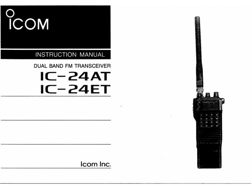
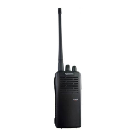
Icom IC-F33GT User manual

S-14113IZ-C1-q
Apr. 2007
VHF TRANSCEIVER
iC-f33gt
iC-f33gs
iC-f34gt
iC-f34gs

This service manual describes the latest service
information for the IC-F33GT/GS and IC-F34GT/GS VHF
TRANSCEIVER at the time of publication.
NEVER connect the transceiver to an AC outlet or to a DC
power supply that uses more than 8 V. This will ruin the
transceiver.
DO NOT expose the transceiver to rain, snow or any liquids.
DO NOT reverse the polarities of the power supply when
connecting the transceiver.
DO NOT apply an RF signal of more than 20 dBm (100 mW) to
the antenna connector. This could damage the transceiver’s
front-end.
To upgrade quality, any electrical or mechanical parts and
internal circuits are subject to change without notice or
obligation.
MODEL VERSION CHANNEL
SPACING
FREQUENCY
RANGE
IC-F33GT
(10-key)
USA-01 15.0/30.0 kHz
136–174 MHz
USA-02
GEN-01 12.5/25.0 kHz
CHN-01
IC-F34GT
(10-key) EUR-01 12.5/20.0/25.0 kHz
IC-F33GS
(4-key)
USA-01 15.0/30.0 kHz
USA-02
GEN-01 12.5/25.0 kHz
CHN-01
IC-F34GS
(4-key)
EUR-01
12.5/20.0/25.0 kHz
SWE-07
SWE-09
NOR-08
Be sure to include the following four points when ordering
replacement parts:
1. 10-digit Icom parts numbers
2. Component name
3. Equipment model name and unit name
4. Quantity required
<ORDER EXAMPLE>
1110003491 S.IC TA31136FNG IC-F33GT MAIN UNIT 5 pieces
8820001210 Screw 2438 screw IC-F33GT Top cover 10 pieces
Addresses are provided on the inside back cover for your
convenience.
Icom, Icom Inc. and logo are registered trademarks of Icom Incorporated (Japan) in the United States, the United
Kingdom, Germany, France, Spain, Russia and/or other countries.
ORDERING PARTS
1. Make sure the problem is internal before disassembling
the transceiver.
2. DO NOT open the transceiver until the transceiver is
disconnected from its power source.
3. DO NOT force any of the variable components. Turn
them slowly and smoothly.
4. DO NOT short any circuits or electronic parts. An
insulated tuning tool MUST be used for all adjustments.
5. DO NOT keep power ON for a long time when the
transceiver is defective.
6. DO NOT transmit power into a Standard Signal
Generator or a Sweep Generator.
7. ALWAYS connect a 50 dB to 60 dB attenuator between
the transceiver and a Deviation Meter or Spectrum
Analyzer when using such test equipment.
8. READ the instructions of test equipment throughly
before connecting a test equipment to the transceiver.
REPAIR NOTES
INTRODUCTION
CAUTION

CONTENTS
SECTION 1 SPECIFICATIONS
SECTION 2 INSIDE VIEWS
SECTION 3 DISASSEMBLY INSTRUCTIONS
SECTION 4 OPTIONAL UNITS INSTALLATION
SECTION 5 CIRCUIT DESCRIPITON
5-1 RECEIVER CIRCUITS. . . . . . . . . . . . . . . . . . . . . . . . . . . . . . . . . . . . . . . . . . . . . . . . . . . . . . . . 5-1
5-2 TRANSMITTER CIRCUITS . . . . . . . . . . . . . . . . . . . . . . . . . . . . . . . . . . . . . . . . . . . . . . . . . . . . 5-2
5-3 FREQUENCY SYNTHSYZER CIRCUITS . . . . . . . . . . . . . . . . . . . . . . . . . . . . . . . . . . . . . . . . . 5-4
5-4 POWER SUPPLY CIRCUITS. . . . . . . . . . . . . . . . . . . . . . . . . . . . . . . . . . . . . . . . . . . . . . . . . . . 5-4
5-5 PORT ALLOCATIONS . . . . . . . . . . . . . . . . . . . . . . . . . . . . . . . . . . . . . . . . . . . . . . . . . . . . . . . . 5-5
SECTION 6 ADJUSTMENT PROCEDURES
6-1 PREPARATION . . . . . . . . . . . . . . . . . . . . . . . . . . . . . . . . . . . . . . . . . . . . . . . . . . . . . . . . . . . . . 6-1
6-2 SOFTWARE ADJUSTMENTS . . . . . . . . . . . . . . . . . . . . . . . . . . . . . . . . . . . . . . . . . . . . . . . . . . 6-4
SECTION 7 PARTS LIST
SECTION 8 MECHANICAL PARTS
SECTION 9 BOARD LAYOUTS
SECTION 10 BLOCK DIAGRAM
SECTION 11 VOLTAGE DIAGRAM
11-1 MAIN UNIT . . . . . . . . . . . . . . . . . . . . . . . . . . . . . . . . . . . . . . . . . . . . . . . . . . . . . . . . . . . . . . . . 11-1
11-2 PA/ANT/FUSE UNITS . . . . . . . . . . . . . . . . . . . . . . . . . . . . . . . . . . . . . . . . . . . . . . . . . . . . . . . . 11-3
SECTION 12 BC-160

1 - 1
SECTION 1 SPECIFICATIONS
■GENERAL
• Frequency coverage : 136.000–174.000 MHz
• Mode : FM
• Type of emission :
• Number of conventional channels : 256 ch, 16 banks
• Antenna impedance : 50 Ω(nominal)
• Operating temperature range : –30˚C to +60˚C (–22˚F to +140˚F) [USA], [GEN]
–25˚C to +55˚C [EUR]
• Power supply requirement : 7.2 V DC nominal (negative ground)
• Current drain (at 7.2 V DC) :
• Dimensions (projections not included) : 53.0(W) × 120.0(H) × 32.5(D) mm; 23⁄32(W) × 423⁄32(H) × 19⁄32(D) in
• Weight (with BP-231+FA-SC55V-1) : 285 g; 101⁄16 oz (Approx.)
■TRANSMITTER
• Output power (at 7.2 V DC) : High: 5 W, Low: 1 W
• Modulation : Variable reactance frequency modulation
• Maximum permissible deviation : ±5.0 kHz (Wide), ±4.0 kHz (Middle), ±2.5 kHz (Narrow)
• Frequency error : ±2.5 ppm
• Spurious emissions : 80 dB (typical) [USA], [GEN]
0.25 µW (≤1 GHz), 1.0 µW (≥1 GHz) [EUR]
• Adjacent channel power : 70 dB min (80 dB typical) for Wide and Middle
60 dB min (70 dB typical) for Narrow
• Audio harmonic distortion : 3% typical (Mod. 1 kHz, 40% deviation)
• Limiting charact of modulator : 60–100% of maximum deviation
• Microphone impedance : 2.2 kΩ
■RECEIVER
• Receive system : Double conversion superheterodyne system
• Intermediate frequencies : 1st IF: 46.35 MHz, 2nd IF: 450 kHz
• Sensitivity : 0.25 µV (–119 dBm) typical at 12 dB SINAD [USA], [GEN]
–4 dBµV (–111 dBm) emf typical at 20 dB SINAD [EUR]
• Adjacent channel selectivity : 70 dB min (75 dB typical) for Wide and Middle
60 dB min (65 dB typical) for Narrow
• Spurious response : 70 dB
• Intermodulation rejection ratio : 70 dB min (74 dB typical) [USA], [GEN]
65 dB min (67 dB typical) [EUR]
• Audio output power : 0.5 W typical at 5% distortion with an 8 Ωload
• Squelch sensitivity (at threshold) : 0.25 µV typical
• Output impedance (Audio) : 8 Ω
Specifications are measured in accordance with EIA-152-C/204D, TIA-603 or EN 300 086.
All stated specifications are subject to change without notice or obligation.
VERSION WIDE MIDDLE NARROW
[USA], [GEN] 16K0F3E (25.0 kHz) N/A 11K0F3E (12.5 kHz)
[EUR] 14K0F3E (20.0 kHz) 8K50F3E (12.5 kHz)
RECEIVING TRANSMITTING
Stand-by Max. audio High (5 W) Low (1 W)
85 mA 300 mA 1.5 A 0.7 A

2 - 1
SECTION 2 INSIDE VIEWS
TX Mute switch
(Q501: UNR9213J)
PLL IC
(IC21: LMX2352TM)
Base band IC
(IC14: AK2346)
EEPROM
(IC10: 24LC64T-I/SN)
CPU
(IC22: HD64F2238BTF13)
R5 Regulator
(Q25: 2SA1577)
FM IF IC
(IC9: TA31136FN)
AF amplifier
(IC15: TA7368F)
APC amplifier
(IC2: TA75S01F) IF amplifier
(Q7: 2SC4215) TX/RX switch
(D16, D17: MA2S077)
+5 Regulator
(IC17: NJM2870)
T5 Regulator
(Q24: 2SA1577)
D/A converter
(IC12: M62364FP)
VCO circuits
TOP VIEW BOTTOM VIEW
S5 Regulator
Q26: 2SB1132
Q27: XP6501
Q28: UNR9113 J
Power amplifier
(Q701: RD07MVS1)
Drive amplifier
(Q702: RD01MUS1)
Antenna switch
(D701: 1SV307)
TOP VIEW BOTTOM VIEW
• MAIN UNIT
• PA UNIT

3 - 1
SECTION 3 DISASSEMBLY INSTRUCTION
• REMOVING THE CHASSIS UNIT
1 Unscrew 1 nut A, and remove 2 knobs B, C.
2 Unscrew 2 screws D.
3 Unscrew 2 screws E.
4 Take off the chassis unit in the direction of the arrow.
5 Unplug the connector Ffrom the chassis unit.
• REMOVING THE PA UNIT
1 Unscrew 3 screws M.
2 Unsolder 4 points N, and take off the PA unit in the
direction of the arrow.
• REMOVING THE MAIN UNIT
1 Unscrew 2 nuts G, and remove the top plate H.
2 Remove the side plate I.
3 Unscrew 6 screws J.
4 Unsolder 8 points K, and remove the main shield.
5 Unsolder 2 points L, and take off the main unit in the
direction of the arrow.
Chassis unit E
A
B
C
D
F
Main shield
Main unit
K
K
J
J
L
J
I
GH
Chassis unit
M
N
N

4 - 1
SECTION 4 OPTIONAL UNIT INSTALLATION
:swoll
ofsati
nulanoi
tpoeht
llatsnI
qetatoR ]LOV[ -
tabe
htevo
m
e
r
d
na,F
FO
re
wopehtnrutot
.kcapyret
w.r
e
v
o
ctinuehtevomeR
:ETON ,
tn
em
ur
t
s
ni
ta
fl
ra
li
m
i
s
aro
r
e
v
i
r
d
w
e
rcs
dae
h
taflaesU
yawae
k
a
t
dnatfilneht
,
si
s
sahcehtfo
wollohehtot
nitresni
dna
.revo
cti
nueht
!rev
oc
t
i
n
uerap
sde
il
ppusehtesU t
a
h
trevoc
eh
t
esu
tonoD
-
s
n
art
e
ht
ot
n
it
e
g
y
am
ts
u
d
r
or
e
t
a
W
.e
c
no
de
v
om
e
r
ne
ebsah
.
no
i
s
ehd
a
s
’tit
s
ol
s
ah
rotneb
eby
amr
ev
oc
ehtesu
ace
br
evi
ec
.dega
mad
gn
ie
b
revie
c
s
nar
t
eh
t
ni
tluser
yamsi
h
T
e.wolebnwohssat
inue
h
tllatsn
I
re
t
at
o
r
n
e
ht
,kca
p
y
r
ett
ab
ehtdn
a
re
vocti
n
u
e
ht
e
c
alp
eR
]
LO
V
[.
NO
re
w
ope
ht
n
r
ut
o
t
:ETO
N
0
1
1
-
T
U
/9
0
1-T
U
l
a
n
o
i
t
p
o
e
hT
ST
I
NU
R
EL
B
M
A
R
C
S
,
5
01-
T
UI
Iknur
T
ra
mS ™
DR
A
O
B
CI
GOL
S
7
1
1
-TU/7
1
1
-
TUr
o
G3
k
nurT
r
a
m
S™
D
R
AOB
CIG
O
L
-
id
om
dr
a
o
b
C
P
em
o
s
seriuq
e
r
on
n
o
i
t
a
l
l
a
t
s
n
i
l
a
noi
t
i
dd
a
eht
o
t
refer
e
s
a
e
lP
.
s
n
o
i
t
a
c
i
f
next page.
sino
i
tar
tsull
i
sihT*
ehthtiwdebircsed
.311
-
TU
noitallatsni011-TUdna901-TU
n
ehw
deri
uqer
si
no
itac
ifid
o
m
d
r
aob
C
P
gniw
ollof
e
hT
:011-TU
r
o
901-TUlan
oi
tpoe
ht
gnilla
ts
ni
qetatoR ]
LOV[ -ta
b
eh
t
ev
om
erdna
,F
FOr
ew
op
eht
nrutot
.
kca
py
ret
wabove.
n
wo
h
s
sa
r
ev
o
c
t
in
u
eh
t
e
vome
R
edna)C
I
M(
t
iuc
r
ic
c
imXT
eht
t
a
BCP
e
ht
no
n
re
ttap
e
h
t
t
u
C
.
wol
e
bnwohs
s
a)CSID(
t
i
u
cricFAXR
rabove.debircsedsati
nurelbmarcsehtllatsnI
teta
to
r
neh
t
,
kc
ap
y
ret
tabeh
t
dnar
e
vocti
nu
ehteca
l
p
eR
]
L
OV[ .N
O
rewo
p
e
ht
n
r
ut
ot
t
i
n
u
r
e
lbm
ar
c
s
eh
t
gnill
atsninun
ehW:ETON
-r
e
h
t
o
,
t
f
e
l
t
a
s
t
n
i
o
p
d
e
t
c
en
noc
side
ht
r
edlos-ero
t
er
us
e
B
.
e
l
b
a
l
i
a
v
a
s
i
t
uptu
oF
A
ronoital
u
domXTonesiw

4 - 2
ne
hw
deriu
qer
si
no
itaci
fid
o
m
dr
aob
CP
gniwoll
of
ehT
:S
71
1-
TU
ro7
1
1-
TU
,501-TUlan
oit
poe
ht
gnilla
tsn
i
qetatoR ]LOV[ -tabehtevomer
d
na,FFOrewopehtnrutot
.
kca
p
yret
wabove.deb
ir
cseds
a
rev
octi
nuehtev
om
e
R
e-
ri
c
FAXRehttaBCPehtnon
r
ettapeht
r
edlo
s
d
n
a
t
u
C
.thgir
t
anwohs
s
atiuc
p
e
t
s
t
x
en
e
hT r.noi
t
al
l
a
t
s
ni
S
7
1
1
-T
Ueh
t
r
o
f
yr
a
ssec
e
n
si
pe
ts
ot
o
Gt.
7
1
1
-T
U
r
o
5
0
1
-
TU
e
h
t
l
l
a
t
sn
i
ot
rdna)CI
M
(tiucr
i
cci
m
X
Tehtta
B
CPe
h
tno
nrett
a
pe
h
t
tuC
.thgi
r
tanwohssa)CSI
D
(
t
iucricF
A
X
R
t1-TU/
5
01-TU
eh
t
l
la
t
snI above.de
bi
rcs
ed
s
a
S711-TU/
71
yetat
o
rneht,kcapyr
e
ttabehtdnarevoct
i
nu
ehte
ca
lpeR
]L
OV
[.NO
r
ewop
e
ht
n
r
ut
ot
G3
knur
Tr
am
Sehtgnilla
t
sninunehW:ETON ™tin
u
s
aC
dna
Br
edl
os-er
dna
,B
dn
aAr
edl
os-nu
o
teru
s
e
B
.elbaliavasituptuoFAonesiwrehto,wolebnwohs
cimXTehtr
e
dlos-erotderiuqersi
S71
1-
TUeht
,
re
voeroM
).CSID(ti
u
c
ri
c
FA
XRdna
)C
IM
(
tiucric
A
B
C
ev
ome
R
A
B
C
e
ryln
o
S71
1
-
T
U
noitallatsniS711-TUdna711-TU,501-TU

4 - 1
SECTION 5 CIRCUIT DESCRIPTION
1ST IF CIRCUITS
The 1st IF circuits consist of 1st mixer, 1st IF filter and 1st IF
amplifier, and converts the received signals into the 1st IF
signal, filters to remove unwanted signals and amplifies.
The RF signals from the bandpass filter are mixed with the
1st LO signals, where come from the RX VCO circuit, at
the 1st mixer circuit (Q6) to produce a 46.35 MHz 1st IF
signal. The 1st IF signal is passed through a monolithic filter
(FI1) to suppress out-of-band signals. The filtered signal is
applied to the 2nd IF circuit after being amplified at the 1st
IF amplifier (Q7).
2nd IF AND FM DEMODULATOR CIRCUITS
The 2nd IF circuits consist of 2nd mixer, 2nd IF filter, 2nd
IF amplifier, and converts the 1st IF signal from the 1st IF
circuits into the 2nd IF signal, filters to remove unwanted
signals and amplifies.
An FM IF detector IC consists of whole of the 2nd IF circuits
and FM demodulator circuit.
The 1st IF signal from the IF amplifier (Q7) is applied to
the 2nd mixer section of the FM IF IC (IC9, pin 16), and is
mixed with the 2nd LO signal to be converted into a 450
kHz 2nd IF signal.
The FM IF IC (IC9) contains the 2nd mixer, limiter amplifier,
quadrature detector, active filter and noise amplifier circuits.
A 2nd LO signal (45.9 MHz) is produced at the PLL circuit
by tripling it’s reference frequency 15.3 MHz).
RX AF CIRCUITS
The AF circuits consist of AF filters, AF amplifier, AF
power amplifier, etc., and amplify, filter the AF signals FM-
demodulated by the FM IF detector IC.
The AF selector changes the destination of the AF signals.
The AF signals from the FM IF IC (IC9, pin 9) are amplified
at the AF amplifier section in the base band IC (IC14, pin
23), and are then applied to the high-pass filter and low-
pass filter section of it.
5-1 RECEIVER CIRCUITS
RF CIRCUITS
RF circuits consist of RF filters, antenna switch, preamplifier,
etc., and extracts and amplifies the signal which is desired to
receive.
An antenna switch toggles RX line and TX line by PIN
diodes.
While receiving, the TX line and the antenna is disconnected
to prevent received signals entering. The RX line is
disconnected from the GND simultaneously, and an
LPF which guides received signals to the RX circuits is
composed.
While transmitting, serial-connected PIN diodes are ON,
thus the TX line is connected to the antenna, and the RX
line is connected to the GND simultaneously to prevent
transmit signal entering.
The tuned-BPF is tuned to a desired frequency to receive by
variable capacitor, and extracts the signal which is desired
to receive.
The signals from the antenna switching circuit pass through
the two-stage tunable bandpass filters (D19, D24, L7, L8,
C27, C369). The filtered signals are amplified at the RF
amplifier (Q5) and then passed through the another two-
stage tunable bandpass filters (D14, D15, L11, C39, C45) to
suppress unwanted signals. The filtered signals are applied
to the 1st mixer circuit.
Received signals enter the antenna connector (CHASSIS;
J1) and pass through the low-pass filter (ANT unit; L801,
L802, C803). The filtered signals are passed through the 1/4
λtype antenna switching circuit (D701, D704, D706) and
then applied to the RF circuit.
D14, D15, D19 and D24 employ varactor diodes, that are
controlled by the CPU via the D/A converter (IC12), to track
the bandpass filter. These varactor diodes tune the center
frequency of an RF passband for wide bandwidth receiving
and good image response rejection.
Mixer
16
Limiter
amp.
2nd IF filter
450 kHz X2
15.3 MHz
45.9 MHz
IC9 TA31136FN
12 1st IF from the IF amplifier (Q7)
"RSSI" signal to the CPU ( IC22, pin 50)
11109
87 5
AF signal "DET"
"SQLC" signal from the
D/A converter IC
(IC12, pin 2)
R5V
X1
2
Active
filter
Noise
detector
FM
detector
13
"NOIS" signal to the CPU (IC22, pin 75)
RSSI
Noise
amp.
Noise
comparator
×3
Q22
FI2
3
• 2nd IF AND FM DEMODULATOR CIRCUITS

4 - 2
The filtered signals pass through the high-pass filter to sup-
press unwanted harmonic components. The signals pass
through (or bypass) scrambler and expander sections. The
signals are amplified at the amplifier section in the base
band IC (IC14).
The output signals from IC14 (pin 20) pass through the low-
pass filter sector (IC23, pins 1, 2), and are then applied to
the AF amplifier (IC15, pin 8) via the AF volume (R315).
The power amplified AF signals are output from pin 10 and
applied to the internal speaker that is connected to J4 via
[SP] jack (J2).
SQUELCH CIRCUITS
• NOISE SQUELCH
The noise squelch cuts off the RX AF line to mute the
AF output signals when no RF signals are received.
Extracting noise components (approx. 30 kHz signal) in the
demodulated AF signals, the squelch circuit turns the AF
power amplifier and AF switches ON and OFF.
The squelch circuits consist of the threshold level adjuster,
noise filter and noise detector.
FM-demodulated AF signals from the FM IF detector IC are
adjusted its level (=squelch threshold level) by DAC (D/A
converter), then passed through the noise filter to extruct
the noise components. The noise components are rectified
by noise detector to produce DC voltage corresponding to
the noise level, then applied to the CPU and compared with
the reference voltage preset in the CPU to control AF power
amplifier and AF switches ON and OFF.
A portion of the AF signals from the FM IF IC (IC9, pin 9)
are passed through the D/A converter (IC12, pins 1, 2). The
signals are applied to the active filter section in the FM IF
IC (IC9, pin 8). The active filter section filters and amplifies
noise components. The amplified signals are converted into
the pulse-type signals at the noise detector section. The
detected signals output from pin 13 (NOIS) via the noise
comparator section.
The “NOIS” signal from the FM IF IC is applied to the CPU
(IC22, pin 75). Then the CPU analyzes the noise condition
and outputs AF mute control signal from pin 84 to control
the squelch switch (Q502) as the “MUTE” signal.
• TONE SQUELCH
The tone squelch connects the RX AF line to emit the AF
output signals only when receiving a signal which consists
of matched tone frequency preset in the CPU.
Detecting CTCSS/DTCS signal in the demodulated AF
signals, the tone squelch circuit turns the AF power amplifier
and AF switches ON and OFF.
FM-demodulated AF signals from the FM IF detector IC are
passed through the tone filter to remove unwanted auible
siganls. then applied to the CPU and compared with the
tone frequency/code preset in the CPU to control AF power
amplifier and AF switches ON and OFF.
A portion of the “DET” AF signals from the FM IF IC (IC9,
pin 9) pass through the low-pass filter (IC19, pin 5) to
remove AF (voice) signals, and are then applied to the
amplifier (IC19, pin 3). The amplified signals are applied to
the CTCSS or DTCS decoder in the CPU (IC22, pin 46) via
the “CDEC” line. The CPU outputs AF mute control signal
from pin 84 to control the squelch switch (Q502) as the
“MUTE” signal.
5-2 TRANSMITTER CIRCUITS
TX AF CIRCUIT
The TX AF circuit consists of microphone amplifier, ALC and
AF filter. ALC (Automatic Level Controller) is an amplifier that
reduces its gain automatically to prevent over deviation. The
AF filter cuts off the signals except voice signals (3 kHz or
higher and 300 Hz or lower).
The AF signals (MIC) from the microphone (MC1) are
applied to the amplifier (IC23, pins 6, 7). The amplified sig-
nals are amplified again at the microphone amplifier section
of the base band IC (IC14, pins 3). The amplified signals
are passed through or bypass the compressor, scrambler
sections of IC14, and are then passed through the high-
pass, limiter amplifier, splatter filter sections of IC14.
The filtered AF signals from the base band IC (pin 6) are
applied to the FM/PM switch (IC13, pins 6, 7), and pass
through the low-pass filter (IC6, pins 1, 2). The filtered sig-
nals are applied to the D/A converter (IC12, pin 4). The out-
put signals from the D/A converter (IC12, pin 3) are applied
to the modulation circuit (D12).
AF signals range of 300 Hz to 3 kHz
Base band IC
(IC14)
"DET" AF signal
from FM IF IC (IC9, pin 9) 23 20 LPF
AF
volume
AF
AMP
IC15
Speaker
IC23
IC23
IC13
IC6 IC12 D12
Microphone
AMP
3
7
4
FM/PM switch
D/A converter FM mod.
LPF
"CTCSS/DTCS" signal from
D/A conveter IC (IC12, pin 11)
"TONE" signal from CPU via low-pass
filter (IC22, pin 43)
to TX VCO circuit
(Q16, D10, D13, D501)
3
• AF CIRCUIT (TX and RX)

4 - 3
MODULATION CIRCUIT
• VOICE SIGNAL
The modulation circuit FM-modulates the VCO oscillating
signal with the AF signals from the TX AF circuit.
The AF signals from the microphone amplifier circuits are
applied to the variable capacitor to change its reactance for
FM modulation.
The AF signals from the D/A converter (IC12, pin 3) change
the reactance of varactor diode (D12) to modulate the oscil-
lated signal at the TX VCO circuit (Q16, D10, D13, D501).
The modulated VCO signal is amplified at the buffer ampli-
fiers (Q15, Q29) and is then applied to the drive amplifier
circuit via the T/R switch (D16).
• TONE SIGNAL
Tone signals are generated in the CPU and applied to the
both of the VCO and reference frequency oscillator to be
modulated.
The CTCSS/DTCS signals (“CENC0,” “CENC1,” ”CENC2”)
from the CPU (IC22, pins 13, 15, 16) are combined at the
resistors (R222–R224) and are then pass through the low-
pass filter (IC6, pins 12, 14). The filtered signals are applied
to the D/A converter (IC12, pin 12) via the “TONC” line. The
output signals from the D/A converter (IC12, pin 11) are
mixed with the filtered Mic audio signals.
The mixed signals are passed through the D/A converter
(IC12, pin 3, 4), and are then applied to the D12 in the TX
VCO circuit.
TRANSMIT AMPLIFIERS
The transmit amplifers consist several RF amplifier
(predriver, driver, power) and amplify the VCO output to the
transmit output level.
APC CIRCUIT
The APC (Automatic Power Control) circuit stabilizes
transmit output power to prevent transmit output power level
change which is caused by load mismatching or heat effect,
etc,. The APC circuit also selects transmit output power from
high, middle and low power.
The power detector rectifies a portion of the transmit output
and converts it into DC voltage which is in proportion to the
transmit output power level. The detected voltage is applied
to the comparator. The transmit power setting voltage is ap-
plied to another input terminal as the reference voltage.
The comparator compares the detected voltage and refer-
ence voltage, and the difference of voltage is output. The
output voltage controls the bias of the RF amplifiers to re-
duce/increase the gain of these amplifiers for stable transmit
output power.
The change of transmit power is carried out by the change
of reference voltage.
The power detector circuit (PA unit; D702, D703) detects the
transmit power output level and converts it into DC voltage.
The output voltage is at a minimum level when the antenna
impedance is matched with 50 Ωand is increased when it is
mismatched.
The detected voltage is applied to the differential amplifier
(MAIN unit; IC2; pin 3), and the “T2” signal from the D/A
converter (MAIN unit; IC12, pin 23), controlled by the CPU
(MAIN unit; IC22), is applied to the other input for reference.
When antenna impedance is mismatched, the detected
voltage exceeds the power setting voltage. Then the output
voltage of the differential amplifier (MAIN unit; IC2, pin 4)
controls the input bias voltage of the drive (PA unit; Q702)
and power (PA unit; Q701) amplifiers to reduce the output
power.
Power
amp.
APC
amp.
Driver
amp.
+
–
YGR
amp.
VCC
to ANT unit
PA unit
T2
TMUT
RF signal
from PLL circuit
T5V
APC control circuit
D703
D702
ANT
SW LPF
LPF
Q702
Q704
IC2
IC501
Q701
D701
• APC CIRCUIT

4 - 4
5-3 FREQUENCY SYNTHESIZER CIRCUITS
VCO
A VCO is an oscillator which its oscillation frequency is
determined by the applied volatge.
Shifting the oscillation frequency range in RX/TX, the VCO
generates both of the TX signal and 1st LO signals.
There are two VCOs; RX VCO and TX VCO. The RX VCO
generates the 1st LO signals for the 1st IF produce, and TX
VCO generates TX signal.
The VCO circuits contains a separate RX VCO (Q17, D9,
D11, D500) and TX VCO (Q16, D10, D13, D501). The oscil-
lated signal is amplified at the buffer amplifiers (Q15, Q29)
and is then applied to the T/R switch (D16, D17). Then the
receive 1st LO (Rx) signal is applied to the 1st mixer (Q6)
and the transmit (Tx) signal to the YGR amplifier circuit (PA
unit; Q704).
A portion of the signal from the buffer amplifier (Q15) is fed
back to the PLL IC (IC21, pin 6) via the doubler circuit (Q14)
as the comparison signal.
PLL (Phase Locked Loop) CIRCUIT
The PLL circuit provides stable oscillation for both of the
transmit frequency and 1st LO frequency for receive. By
comparing feedbacked VCO output and reference frequency
signal and adjusting the differences.
The PLL output frequency is controlled by the serial data
including divid ratio from the CPU.
A portion of VCO output is applied to the PLL IC via buffer
and harmonic filter. The applied VCO output is divided
according to the serial data including divid ratio from
the CPU, at the prescaler and programmable divider. In
the same way, the reference frequency signal from the
reference frequency signal oscillator is applied to the PLL
IC and divide so that these are the same frequency.
The VCO output and the reference frequency signals
divide and frequency-matched are applied to the phase
comparator and phase-compared. The resulted phase
difference is detected as a phase-type signal, and level-
adjusted at the charge pump then output. The output pulse
type signal is passed through the loop filter to be converted
into the DC voltage (=Lock Voltage).
Applying the lock voltage to the variable capacitor which
composes a part of the resonator of VCO, the capasitance
of VD changes corresponding to the appled lock voltage.
This causes the change of resonation frequency that
determine the VCO oscilation frequency to keep the VCO
frequency constant.
The PLL circuit contains the TX and RX VCO circuits (Q16,
Q17, D9–D11, D13, D500, D501). The oscillated signal is
amplified at the buffer amplifier (Q15). The output signal fre-
quency is doubled at Q14, and is then applied to the PLL IC
(IC21, pin 6) after being passed through the bandpass filter
(L32, C205, C507).
Q500, D502 and D503 switch the filtering frequencies
between TX and RX which is controlled by R5V.
When the oscillation frequency drifts, its phase changes
from that of the reference frequency, causing a lock voltage
change to compensate for the drift in the VCO oscillating
frequency.
Shift register
Prescaler
Phase
detector
Loop
filter
Programmable
counter
Programmable
divider
X2
15.3 MHz
10
Buffer
Q15
Buffer
Q21
Buffer
Q29
×2
Q14
14
15
16
SCK
SO
PLST
to transmitter circuit
to 1st mixer circuit
D16
D17
46
Q16, D10, D13, D501
TX VCO
Q17, D9, D11, D500
RX VCO
IC21 LMX2352
3
45.9 MHz 2nd LO
signal to the FM IF IC
(IC9, pin 2) Tripler
Q22
"LVIN" signal
to the CPU
(IC22, pin 49)
BPF
• FREQUENCY SYNTHESIZER CIRCUITS
5-4 POWER SUPPLY CIRCUIT
LINE DESCRIPTION
VCC The voltage from the connected battery pack.
+5V Common 5 V converted from the VCC line at the +5 regulator circuit (IC17). The output voltage is supplied to the buf-
fer amplifiers (Q21), PLL IC (IC21) etc.
S5V Common 5 V converted from the VCC line at the S5 regulator circuit (Q26–Q28). The output voltage is supplied to
the ripple filter (Q20), etc.
R5V Receive 5 V converted from the S5V line at the R5 regulator circuit (Q25). The output voltage is supplied to the tripler
(Q22), FM IF IC (IC9), IF amplifier (Q7), 1st mixer (Q6), RF amplifier (Q5), etc.
T5V
Transmit 5 V converted from the S5V line at the T5 regulator circuit (Q24). The output voltage is supplied to the APC
amplifier (IC2), PA unit, etc.

4 - 6
Pin
number
Port
name Description
13, 15,
16
CENC0–
CENC2
Output the CTCSS/DTCS signals.
29 REF
Outputs the reference oscillator cor-
recting voltage. The voltage is applied
to the buffer amplifier (IC24, pin 3)
30 PLST Outputs strobe signals to the PLL IC
(IC21, pin 16).
34 PMFM
Outputs the FM/PM modulation
switching signal to the FM/PM switch
(IC13, pin 5).
35 MDIO
I/O port for the serial data signals
from/to the base band IC (IC14,
pin 11).
36 MSCK Outputs clock signal for the base
band IC (IC14, pin 13).
37 MDIR Outputs serial data control signal to
the base band IC (IC14, pin 14).
38 MTCK
Input port for transmitting MSK clock
signal from the base band IC (IC14,
pin 9).
39 MTDT Outputs MSK data for transmitting to
the base band IC (IC14, pin 10).
40 MRDF
Input port for the receiving MSK de-
tection signal from the base band IC
(IC14, pin 12).
41 DAST Outputs strobe signals to the D/A
convertor (IC12, pin 6).
43 SENC Output single tone encoder signal.
44 BEEP Outputs beep audio signals.
45 SDEC
Input port for single tone decode
signal from the base band IC (IC14,
pin 21).
Pin
Number
Port
name Description
46 CDEC Input port for CTCSS/DTCS signal
from the amplifier (IC19, pin 1).
48 BATV Input port for the detect signal for
connecting battery pack’s voltage.
49 LVIN Input port for the PLL lock voltage.
50 RSSI Input port for the S-meter signal from
the FM IF IC (IC9, pin 12).
51 TEMP Input port for the transceiver’s internal
temperature detecting signal.
69 CSFT Outputs shift signal for reference os-
cillator’s frequency.
70 AFON
Outputs audio control signal.
Low: While outputs audio signals
from the speaker.
74 PTT
Input port for the PTT switch detec-
tion signal.
Low: While the PTT switch is
pushed.
75 NOIS Input port for the noise signal from
the FM IF IC (IC9, pin 13).
76 SO
Outputs serial data to the PLL IC
(IC21, pin 15) and D/A convertor
(IC12, pin 8).
78 SCK
Outputs serial clock signal to the PLL
IC (IC21 pin 14), D/A convertor (IC12,
pin 7), etc.
79 CLI Input port for the cloning data signal.
80 CLO Outputs the cloning data signal.
82 ESDA I/O port for data signals from/to the
EEPROM (IC10, pin 5).
84 MUTE Outputs AF control signal .
Low: While Squelch ON.
85 ESCL Outputs clock signal to the EEPROM
(IC10, pin 6).
86 S5C
Outputs the S5 regulator (Q26–Q28)
control signal.
Low: While the S5 regulator out-
puts 5 V voltage.
87 T5C
Outputs the T5 regulator (Q24) con-
trol signal.
Low: While transmitting.
88 R5C
Outputs the R5 regulator (Q25) con-
trol signal.
Low: While receiving.
89 TMUT
Outputs the transmitting mute switch
control signal to the mute switch
(Q 501).
High: While muting.
90 ULCK Input port for the PLL unlock signal.
Low: The PLL circuit is unlocked.
5-6-2 CPU (MAIN unit; IC22)
Pin
Number
Port
name Description
10 BAL
Outputs the modulation balance level
control signal. The signal is applied to
the buffer amplifier (IC24, pin 1).
14 TLVA Outputs the TX VCO lock voltage
control signal.
15 RLVA Outputs the RX VCO lock voltage
control signal.
22 T1
Outputs the bandpass filter tuning
control signal . The output signal is
applied to the bandpass filters (D19,
D240).
23 T2
• Outputs the bandpass filter tuning
control signal . The output signal is
applied to the bandpass filters (D14,
D15).
• Outputs the TX control signal . The
output signal is applied to the APC
amplifier (IC2, pin 1).
5-6 PORT ALLOCATIONS
5-6-1 D/A CONVERTOR IC (IC12)

6 - 1
SECTION 6 ADJUSTMENT PROCEDURE
EQUIPMENT GRADE AND RANGE EQUIPMENT GRADE AND RANGE
DC power supply Output voltage
Current capacity
: 7.2 V DC
: 5 A or more Audio generator Frequency range
Measuring range
: 300–3000 Hz
: 1–500 mV
FM deviation meter Frequency range
Measuring range
: DC–800 MHz
: 0 to ±10 kHz Attenuator Power attenuation
Capacity
: 20 or 30 dB
: 10 W
Frequency counter
Frequency range
Frequency accuracy
Sensitivity
: 0.1–300 MHz
: ±1 ppm or better
: 100 mV or better
Standard signal
generator (SSG)
Frequency range
Output level
: 100–800 MHz
: 0.1 µV to 32 mV
(–127 to –17 dBm)
Digital multimeter Input impedance : 10 MΩ/V DC or better AC millivoltmeter Measuring range : 10 mV–10 V
RF power meter
Measuring rang
Frequency range
Impedance
SWR
: 1–10 W
: 100–800 MHz
: 50 Ω
: Better than 1.2 : 1
Oscilloscope Frequency rang
Measuring range
: DC–20 MHz
: 0.01–20 V
6-1 PREPARATION
When adjusting IC-F33GT/GS/F34GT/GS, optional CS-F33G ADJ ADJUSTMENT SOFTWARE (Rev. 1.0 or later), OPC-478 CLONING
CABLE (RS-232C type), OPC-478U/UC CLONING CABLE (USB type) and a JIG CABLE (see illustration at page 6-2) are required.
▄SYSTEM REQUIREMENTS
• Microsoft®Windows®98/98SE/Me/2000
• RS-232C serial port (D-sub 9 pin)
• USB port
▄ ADJUSTMENT SOFTWARE INSTALLATION
qBoot up Windows.
- Quit all applications when Windows is running.
wInsert the cloning software CD into the appropriate CD
drive.
eSelect ‘Run’ from the [Start] menu.
rType the setup program name using the full path name,
then push [Enter] key.
(For example; D:\Setup.exe)
tFollow the prompts.
yProgram group ‘CS-F33G ADJ’ appears in the ‘Programs’
folder of the [Start] menu.
▄ BEFORE STARTING SOFTWARE ADJUSTMENT
Program the adjustment frequencies into the transceiver
using with the CS-F33G before starting the software adjust-
ment. Otherwise, the transceiver can not start software ad-
justment.
CAUTION!: BACK UP the originally programmed mem-
ory data in the transceiver before program-
ming the adjustment frequencies.
When program the adjustment frequencies into
the transceiver, the transceiver’s memory data
will be overwritten and lose original memory
data at the same time.
Microsoft and Windows are registered trademarks of Micro-
soft Corporation in the U.S.A. and other countries.
▄
STARTING SOFTWARE ADJUSTMENT
qConnect the transceiver and PC with the OPC-478/U and
JIG CABLE.
wTurn the transceiver power ON.
eBoot up Windows, and click the program group ‘CS-F33G
ADJ’ in the ‘Programs’ folder of the [Start] menu, then CS-
F33G ADJ’s window appears.
rClick ‘Connect’ on the CS-F33G’s window, then appears
the transceiver’s adjustment screen.
tSet or modify adjustment data as desired.
▄ REQUIRED TEST EQUIPMENT
CH FREQUENCY ADJUSTMENT ITEM
1 155.000 MHz TX power
Bandwidth
: High
: Wide
2 155.000 MHz TX power
Bandwidth
: Low 2
: Wide
3 155.000 MHz TX power
Bandwidth
: Low
: Wide
4 155.000 MHz TX power
Bandwidth
: High
: Narrow
5 136.000 MHZ TX power
Bandwidth
: High
: Wide
6 155.000 MHz
TX power
CTCSS
DTCS
Bandwidth
: High
: 151.4 Hz
: 007
: Wide
7 174.000 MHz TX power
Bandwidth
: High
: Wide
8 155.000 MHz TX power
Bandwidth
: High
: Middle
• ADJUSTMENT FREQENCY LIST

6 - 2
FM
deviation meter
SINAD meter
Speaker (8 ½)
Audio generator
AC millivoltmeter
to the antenna connector
Attenuator
20 dB or 30 dB
RF power meter
0.1Ð10 W/50 ½
Frequency
counter
Standard signal generator
0.1 µV to 32 mV
(Ð127 dBm to Ð17 dBm)
CAUTION!
DO NOT transmit while
an SSG is connected to
the antenna connector.
OPC-478
to RS-232C port
To [SP]
IC-F33G/F34G
To [MIC]
Personal
computer
JIG cable
OPC-478/OPC478U
JIG cable
To IC-F33G/F34G
[SP] jack
3-conductor 3.5(d) mm (1⁄8") plug
(SP + )
(CLONE)
(GND)
(SPE − )

6 - 3
• CS-F33G ADJ'S SCREEN EXAMPLE
q: Transceiver's connection state
w: Reload adjustment data
e: Receive sensitivity measurement
r: Connected DC voltage measurement
t: PLL lock voltage measurement
y: Operating channel select
u: RF output power
i: FM modulation balance (Narrow)
o: FM deviation (Narrow)
!0: FM deviation (Wide)
NOTE:
!1: CTCSS/DTCS deviation
!2: Squelch level
!3: Reference frequency
!4: Receive sensitivity (automatic)
!5: PLL lock voltage for RX (automatic)
!6: PLL lock voltage for TX (automatic)
!7: PLL lock voltage for RX (manual)
!8: PLL lock voltage for TX (manual)
!9: S-meter adjustment
The above values for settings are example only.
Each transceiver has its own specific values for each setting.
r
t
y
u
q
i
o
!0
!1
!4
!3
!2
!5
!6 !7
!8
!9
w
e

6 - 4
ADJUSTMENT ADJUSTMENT CONDITION MEASUREMENT VALUE
UNIT LOCATION
PLL LOCK
VOLTAGE
[LV (RX LVA)]
[LV (TX LVA)]
1 • Operating Channel : CH7
• Receiving
PC
screen
Check the "LVIN" item on the
CS-F33G ADJ's screen.
3.5 V
3.5 V
2 • Operating Channel : CH7
• Transmitting
CONVENIENT:
The PLL lock voltage can be adjustment automatically.
Set the cursor to "RX LVA"/"TX LVA" and then push [ENTER] key.
3 • Operating Channel : CH5
• Receiving
PC
screen
Check the "LVIN" item on the
CS-F33G ADJ's screen.
1.0–1.6 V
(Verify)
4 • Operating Channel : CH5
• Transmitting
1.0–1.6 V
(Verify)
REFERENCE
FREQUENCY
[REF]
1 • Operating Channel : CH7
• Connect the RF power meter or 50 Ω dummy
load to the antenna connector.
• Transmitting
Top
panel
Loosely couple the frequency
counter to the antenna con-
nector.
174.0000 MHz
OUTPUT
POWER
[Power (Hi)]
1 • Operating Channel : CH1
• Transmitting
Top
panel
Connect the RF power meter
to the antenna connector.
5.0 W
[Power (L2)] 2 • Operating Channel : CH2
• Transmitting
2.0 W
[Power (L1)] 3 • Operating Channel : CH3
• Transmitting
1.0 W
MODULATION
BALANCE
[BAL]
1 • Operating Channel : CH4
• No audio applied to the [MIC] connector.
• Set the FM deviation meter as:
HPF : OFF
LPF : 20 kHz
De- emphasis : OFF
Detector : (P–P)/2
• Push [P0] while transmitting
Top
panel
Connect the FM deviation
meter with the oscilloscope
to the antenna connector
through the attenuator.
Set to square wave
form
FM
DEVIATION
[MOD N]
(Narrow)
1• Operating Channel : CH4
• Set the FM deviation meter as:
HPF : OFF
LPF : 20 kHz
De- emphasis : OFF
Detector : (P–P)/2
• Connect the audio generator to the [MIC]
connector and set as
: 1.0 kHz/150 mVrms
• Transmitting
Top
panel
Connect the FM deviation
meter to the antenna connec-
tor through the attenuator.
±2.10 kHz
[MOD Ratio]
(Wide)
2• Operating Channel : CH1
• Transmitting
±4.10 kHz
[MOD Ratio]
(Middle)
(F34G only)
3• Operating Channel : CH8
• Transmitting
±3.20 kHz
CTCSS/DTCS
DEVIATION
[CTCSS/DTCS]
1• Operating Channel : CH6
• No audio applied to the [MIC] connector.
• Transmitting
Top
panel
Connect the FM deviation
meter to the antenna connec-
tor through the attenuator.
±0.70 kHz
FREQUENCY
DEVIATION 1 -Operating Channel : CH16 (156.800MHz)
-Output power : Low
-Connect an audio generator to the microphone
connector and set as ;
Frequency : 1kHz
Level : 30mV
-Set the FM deviation meter as ;
HPF : OFF
LPF : 20kHz
De-emphasis : OFF
Detector : (P-P)/2
-Transmitting
Rear
Panel
Connect an FM deviation meter to
the antenna connector through an
attenuator.
±4.25-4.35kHz
6-2 SOFTWARE ADJUSTMENT (TRANSMITTING)
Select an operation using [↑] / [↓]keys, then set specified value using [←] / [→] keys on the connected computer keyboard

6 - 5
ADJUSTMENT ADJUSTMENT CONDITION MEASUREMENT VALUE
UNIT LOCATION
RX
SENSITIVITY
[BPF T1]
[BPF T2]
1• Operating Channel : CH5
• Connect the SSG to the antenna connector
and set as:
Frequency : 136.000 MHz
Level : 10 µV* (–87 dBm)
Modulation : 1 kHz
Deviation : ±3.5 kHz
• Receiving
PC
screen
Connect the SINAD meter
with an 8 Ωload to the [SP]
jack through the JIG cable.
Minimum distortion
level
CONVENIENT:
The BPF T1, BPF T2 can be adjustment automatically.
q-1: Set the cursor to "BPF ALL" and then push [ENTER] key.
q-2: The connected PC tunes BPF T1, T2 to peak levels.
or
w-1: Set the cursor to one of BPF T1, T2 as desired.
w-2: Push [ENTER] key to start tuning.
w-3: Repeat w-1 and w-2 to perform additional BPF tuning.
S-METER
[S-METER] 1• Operating Channel : CH5
• Connect the SSG to the antenna connector
and set as:
Frequency : 136.000 MHz
Level : 14 µV* (–84 dBm)
Modulation : 1 kHz
Deviation : ±3.5 kHz
• Receiving
Push the [ENTER] key on the connected computer's key-
board to set "L2" level.
2• Set the SSG as:
Level : 0.45 µV* (–114 dBm)
• Receiving
Push the [ENTER] key on the connected computer's key-
board to set "L0" level.
SQUELCH
LEVEL
[SQL]
1 • Operating Channel : CH1
• Connect the SSG to the antenna connector
and set as:
Frequency : 155.000 MHz
Level : 0.2 µV* (–121 dBm)
Modulation : 1 kHz
Deviation : ±3.5 kHz
• Receiving
Side
panel
Connect speaker to the [SP]
jack through the JIG cable.
Set SQL level to
close squelch.
Then set SQL level
at the point where
the audio signals
just appears.
*The output level of the standard signal generator (SSG) is indicated as the SSG's open circuit.
SOFTWARE ADJUSTMENT (RECEIVING)
• Select an operation using [↑] / [↓]keys, then set specified value using [←] / [→] keys on the connected computer keyboard
• Need to adjust "S-METER ADJUSTMENT" after "RX SENSITIVITY ADJUSTMENT" is adjusted.
Otherwise , "S-METER ADJUSTMENT" will not be adjusted properly.

7 - 1
SECTION 7 PARTS LIST
M.=Mounted side (T: Mounted on the Top side, B: Mounted on the Bottom side)
[MAIN UNIT]
REF ORDER DESCRIPTION M. H/V
NO. NO.
LOCATION
IC2 1110002751 S.IC TA75S01F (TE85R,F) T 88.1/12.4
IC6 1110005340 S.IC NJM12902V-TE1 B 55.4/23.8
IC8 1110005771 S.IC S-80942CNMC-G9CT2G B 20.8/41.5
IC9 1110003201 S.IC TA31136FNG (EL) T 81.5/17
IC10 1130011581 S.IC 24LC64T-I/SN G B 29.7/13.2
IC12 1190001350 S.IC M62364FP 600D B 38.9/26.2
IC13 1130006221 S.IC TC4W53FU (TE12L,F) B 47.1/24
IC14 1110006221 S.IC AK2346P-E2/P B 41.5/13.2
IC15 1110001811 S.IC TA7368FG (5,ER) T 97.3/15.4
IC17 1110005350 S.IC NJM2870F05-TE1 B 93.2/20.2
IC19 1110005330 S.IC NJM12904V-TE1-
q, w, e, y, u, iB 42.9/39.6
1110006380 S.IC LM2904PWR
r, t, o, !0, !1, !2, !3 B 42.9/39.6
IC20 1130009090 S.IC LC75834W-TLM-E T 57.3/20.3
IC21 1130010100 S.IC LMX2352TMX/NOPB T 79.5/34.1
IC22 1140011511 S.IC HD64F2238BTF13V
r, t, o, !0, !3 only B 17.4/22.4
IC23 1110005330 S.IC NJM12904V-TE1
q, w, e, y, u, iB 36.9/39.3
1110006380 S.IC LM2904PWR
r, t, o, !0, !1, !2, !3 B 36.9/39.3
IC24 1110002751 S.IC TA75S01F (TE85R,F) B 56.2/36.9
IC25 1130007021 S.IC TC7S66FU (TE85L,F) B 58.2/33
Q2 1590003321 S.FET TPC6103 (TE85L,F) T 98.4/4.8
Q3 1590003290 S.TR UNR9213J-(TX) T 93.4/5
Q4 1560000841 S.FET 2SK1829 (TE85R,F) T 90.9/34.7
Q5 1580000731 S.FET 3SK293 (TE85L,F) B 90.9/39
Q6 1580000760 S.FET 3SK299-T1 U73 B 86.8/29.5
Q7 1530002601 S.TR 2SC4215-O (TE85R,F) B 89.2/19.7
Q14 1530003260 S.TR 2SC5006-T1 B 78.7/34.3
Q15 1530003260 S.TR 2SC5006-T1 B 74.9/28.1
Q16 1530003260 S.TR 2SC5006-T1 B 76.6/25.1
Q17 1530003260 S.TR 2SC5006-T1 B 76.1/33.9
Q18 1590001400 S.TR XP1214 (TX) T 73.7/27.9
Q19 1590003290 S.TR UNR9213J-(TX) T 73.9/25.6
Q20 1530002851 S.TR 2SC4116-BL (TE85R,F) T 86.5/25.6
Q21 1560000541 S.FET 2SK880-Y (T5RICOM,F) T 70.8/23.8
Q22 1530002851 S.TR 2SC4116-BL (TE85R,F) T 81.3/24.3
Q24 1510000920 S.TR 2SA1577 T106 Q B 63.3/14.3
Q25 1510000920 S.TR 2SA1577 T106 Q B 64.4/10.4
Q26 1520000450 S.TR 2SB1132 T100 Q B 56.6/11.3
Q27 1590001190 S.TR XP6501-(TX) .AB B 57.5/7.3
Q28 1590003230 S.TR UNR9113J-(TX) B 54.1/7.1
Q29 1530003260 S.TR 2SC5006-T1 B 78.8/23.1
Q38 1590003290 S.TR UNR9213J-(TX) B 81.8/39.2
Q40 1590003290 S.TR UNR9213J-(TX) B 49.5/18.4
Q41 1590001190 S.TR XP6501-(TX) .AB T 90.8/21.3
Q42 1520000450 S.TR 2SB1132 T100 Q T 89.3/17.2
Q43 1590003380 S.TR UNR9111J-(TX) except
q, w, yT 77.7/4.9
1590003400 S.TR UNR9112J q, w, yT 77.7/4.9
Q44 1590003270 S.TR UNR9210J-(TX) B 29.8/5.8
Q45 1590003230 S.TR UNR9113J-(TX) T 54.6/4.5
Q500 1590003290 S.TR UNR9213J-(TX) T 78.6/23.7
Q501 1590003290 S.TR UNR9213J-(TX) T 84.7/11.9
Q502 1560001360 S.FET 2SK3019 TL B 36/11.7
Q503 1590003290 S.TR UNR9213J-(TX)
r, t, o, !0, !1, !2, !3 only T 81.9/42.8
D5 1160000060 S.DIO DAN202U T106 T 93.6/7.3
D6 1790001260 S.DIO MA2S077-(TX) B 27.6/31
D8 1790001250 S.DIO MA2S111-(TX) T 86.7/28.6
D9 1750000771 S.VCP HVC376BTRF-E
r, t, o, !0, !3 only B 69.4/30.5
D10 1750000771 S.VCP HVC376BTRF-E
r, t, o, !0, !3 only B 69.1/26.5
D11 1750000721 S.VCP HVC375BTRF-E
r, t, o, !0, !3 only B 73.3/33.7
D12 1720000471 S.VCP 1SV239 (TPH3,F) B 72/28.4
D13 1750000721 S.VCP HVC375BTRF-E
r, t, o, !0, !3 only B 73.5/23.1
D14 1750000711 S.VCP HVC350BTRF-E
r, t, o, !0, !3 only B 86.1/35.4
D15 1750000711 S.VCP HVC350BTRF-E
r, t, o, !0, !3 only B 87.4/39.5
D16 1790001260 S.DIO MA2S077-(TX) B 84.3/18
D17 1790001260 S.DIO MA2S077-(TX) B 83.4/22.2
D18 1790001250 S.DIO MA2S111-(TX) T 92.9/36.6
D19 1750000721 S.VCP HVC375BTRF-E
r, t, o, !0, !3 only B 94.8/39.1
D20 1790001240 S.DIO MA2S728-(TX) B 94.9/33.4
D21 1160000060 S.DIO DAN202U T106 B 28.4/22.6
D24 1750000721 S.VCP HVC375BTRF-E
r, t, o, !0, !3 only B 96.6/37.7
D25 1790001240 S.DIO MA2S728-(TX) B 94.9/34.7
D28 1790001670 S.DIO RB706F-40T106 B 29.8/2.9
D500 1750000771 S.VCP HVC376BTRF-E
r, t, o, !0, !3 only B 68.2/32.2
D501 1750000771 S.VCP HVC376BTRF-E
r, t, o, !0, !3 only B 68.1/24.9
D502 1790001260 S.DIO MA2S077-(TX) B 79.9/28.1
D503 1790001260 S.DIO MA2S077-(TX) T 80.2/26.7
D504 1750000940 S.DIO ISS400 TE61 B 28.2/24.5
D506 1790000620 S.DIO MA77 (TX)
r, t, o, !0, !1, !2, !3 B 45.4/35.3
S.=Surface mount
[MAIN UNIT]
REF ORDER DESCRIPTION M. H/V
NO. NO.
LOCATION
FI1 2030000150 S.MLH FL-335 (46.350 MHz) T 91.3/27.1
FI2 2020001530 CER CFWLB450KFFA-B0
X1 6070000191 S.DCR CDBKB450KCAY24-R0 B 80/16.9
X2 6050011931 S.XTL CR-781A (15.3 MHz)
B 63.3/38.3
X5 6050011730 S.XTL CR-765 (3.6864 MHz) B 38.3/4
X6 6050011830 S.XTL CR-774 (12.288 MHz) B 30.9/31.5
L7 6200008090 S.COL LQW2BHN68NJ03L B 99.2/38.1
L8 6200008090 S.COL LQW2BHN68NJ03L B 93.1/40.3
L9 6200007750 S.COL LQW2BHN56NJ03L B 88.7/36.5
L11 6200007750 S.COL LQW2BHN56NJ03L B 85.9/33.8
L12 6200009351 S.COL ELJRE R22GFA B 84.3/26.5
L13 6200007850 S.COL ELJNC R82K-F B 89.4/32
L21 6200011031 S.COL ELJRF R10JFB B 80.5/22.8
L22 6200011031 S.COL ELJRF R10JFB B 77.2/28.5
L24 6200003640 S.COL MLF1608E 100K-T B 70.3/26.6
L25 6200007760 S.COL LQW2BHN82NJ03L B 71.9/23.5
L27 6200003550 S.COL MLF1608A 4R7K-T T 68.7/26.7
L28 6200003550 S.COL MLF1608A 4R7K-T T 68.8/30.4
L31 6200007001 S.COL ELJRE 82NGFA B 95.3/31.3
L32 6200007911 S.COL ELJRF 18NJFB T 77.8/27.4
L33 6200004480 S.COL MLF1608D R82K-T T 81.4/22.4
L35 6200003540 S.COL MLF1608D R22K-T T 84.6/25.5
L37 6200008090 S.COL LQW2BHN68NJ03L B 71.6/33.4
L41 6200007911 S.COL ELJRF 18NJFB B 80.2/33.5
L42 6200003550 S.COL MLF1608A 4R7K-T T 71.2/34.2
L43 6200003550 S.COL MLF1608A 4R7K-T T 69.4/21.9
L47 6200007720 S.COL LQW2BHN33NJ03L B 69.1/34.3
L48 6200008090 S.COL LQW2BHN68NJ03L B 69.3/22.7
L500 6200003640 S.COL MLF1608E 100K-T B 70.6/30.4
L501 6200003960 S.COL MLF1608A 1R0K-T T 74.7/31.9
L502 6200011001 S.COL ELJRF 56NJFB B 86.3/25.4
R1 7030005530 S.RES ERJ2GEJ 100 X (10) T 87.4/14.6
R4 7030007570 S.RES ERJ2GEJ 122 X (1.2 k) T 86.3/9.7
R5 7030007340 S.RES ERJ2GEJ 153 X (15 k) T 86.6/8.1
R6 7030005070 S.RES ERJ2GEJ 683 X (68 k) T 86/15.7
R7 7030005310 S.RES ERJ2GEJ 124 X (120 k) T 85.5/13.4
R8 7030005110 S.RES ERJ2GEJ 224 X (220 k) T 88/10.2
R9 7030004980 S.RES ERJ2GEJ 101 X (100) q, w, yT 90.5/12.3
7030004990 S.RES ERJ2GEJ 221 X (220)
except
q, w, yT 90.5/12.3
R12 7030005530 S.RES ERJ2GEJ 100 X (10) B 90.2/36.8
R13 7030005090 S.RES ERJ2GEJ 104 X (100 k) T 95.2/40.2
R15 7030005310 S.RES ERJ2GEJ 124 X (120 k) T 92.2/39.3
R16 7030008280 S.RES ERJ2GEJ 271 X (270) B 89.8/41.2
R17 7030004970 S.RES ERJ2GEJ 470 X (47) T 88.7/36.8
R18 7030005040 S.RES ERJ2GEJ 472 X (4.7 k) T 70.8/30.1
R19 7030005090 S.RES ERJ2GEJ 104 X (100 k) T 91.1/37.6
R21 7030005090 S.RES ERJ2GEJ 104 X (100 k) T 87.3/41.4
R22 7030005050 S.RES ERJ2GEJ 103 X (10 k) T 88.5/38.9
R23 7030005090 S.RES ERJ2GEJ 104 X (100 k) T 86.5/35.6
R24 7030005120 S.RES ERJ2GEJ 102 X (1 k) B 86.2/22.8
R25 7030005120 S.RES ERJ2GEJ 102 X (1 k) B 85.7/31.2
R29 7030007270 S.RES ERJ2GEJ 151 X (150) B 89.2/27.5
R31 7030004980 S.RES ERJ2GEJ 101 X (100) T 89.2/33.7
R32 7030010040 S.RES ERJ2GEJ-JPW T 92.2/31.9
R33 7030007280 S.RES ERJ2GEJ 331 X (330) B 90.2/22.9
R34 7030005090 S.RES ERJ2GEJ 104 X (100 k) B 88.6/21.6
R35 7030004980 S.RES ERJ2GEJ 101 X (100) B 87.2/21.2
R36 7030005030 S.RES ERJ2GEJ 152 X (1.5 k) B 81.9/12.6
R38 7030005090 S.RES ERJ2GEJ 104 X (100 k) T 81.8/12.2
R39 7030004970 S.RES ERJ2GEJ 470 X (47) B 81.4/11.6
R40 7030007270 S.RES ERJ2GEJ 151 X (150) T 81.8/21.3
R43 7030004970 S.RES ERJ2GEJ 470 X (47) T 77.8/14.1
R44 7030005240 S.RES ERJ2GEJ 473 X (47 k) T 77.9/21.3
R45 7030008290 S.RES ERJ2GEJ 183 X (18 k) T 77.2/17.9
R46 7030005000 S.RES ERJ2GEJ 471 X (470) T 76.6/20.7
R48 7030005010 S.RES ERJ2GEJ 681 X (680) B 87.2/19.9
R50 7030005120 S.RES ERJ2GEJ 102 X (1 k) B 84.9/22.8
R68 7030005120 S.RES ERJ2GEJ 102 X (1 k) B 85.6/15.9
R69 7030005050 S.RES ERJ2GEJ 103 X (10 k) B 85.6/18.2
R70 7030004980 S.RES ERJ2GEJ 101 X (100) B 80.1/26.4
R71 7030005070 S.RES ERJ2GEJ 683 X (68 k) B 80.1/25.5
R72 7030005090 S.RES ERJ2GEJ 104 X (100 k) B 35.5/34.2
R73 7030008010 S.RES ERJ2GEJ 123 X (12 k) B 39.1/19.5
R74 7030006610 S.RES ERJ2GEJ 394 X (390 k) B 40.1/19.5
R75 7030005240 S.RES ERJ2GEJ 473 X (47 k) B 78.5/31
R76 7030004980 S.RES ERJ2GEJ 101 X (100) B 78.7/32
R77 7030004980 S.RES ERJ2GEJ 101 X (100) B 77.2/30.9
R78 7030005090 S.RES ERJ2GEJ 104 X (100 k) B 75.9/29.7
R79 7030008340 S.RES RR0510P-182-D (1.8 k) B 76.1/32.4
R80 7030005050 S.RES ERJ2GEJ 103 X (10 k) T 75.1/23.9
R81 7030005090 S.RES ERJ2GEJ 104 X (100 k) B 47.9/20.8
R82 7030009320 S.RES ERJ2GEJ 4R7 X (4.7) B 74.8/25.7
R83 7030008340 S.RES RR0510P-182-D (1.8 k) B 75.3/23.9
R84 7030011000 S.RES RR0510P-392-D (3.9 k) B 74.6/22.7
R85 7030011000 S.RES RR0510P-392-D (3.9 k) B 73.5/29.7
R86 7030005090 S.RES ERJ2GEJ 104 X (100 k) T 71.5/25.8
R87 7030005000 S.RES ERJ2GEJ 471 X (470) B 75.4/31.2
R88 7030008370 S.RES ERJ2GEJ 561 X (560) B 75.1/26.6
R89 7030005050 S.RES ERJ2GEJ 103 X (10 k) T 70.2/25.6
R90 7030005110 S.RES ERJ2GEJ 224 X (220 k) T 71.3/21
R91 7030005060 S.RES ERJ2GEJ 333 X (33 k) T 70.7/19.7
q: GT [USA-01] w: GT [GEN-01] e: GT [EUR-01] r: GT [USA-02] t: GT [CHN-01]
y: GS [USA-01] u: GS [GEN-01] i: GS [EUR-01] o: GS [USA-02] !0: GS [USA-01]
!1: GS [CHN-01] !2: GS [SWE-07] !3: GS [NOR-08] !4: GS [SWE-09]

7 - 2
M.=Mounted side (T: Mounted on the Top side, B: Mounted on the Bottom side)
[MAIN UNIT]
REF ORDER DESCRIPTION M. H/V
NO. NO.
LOCATION
R92 7030005090 S.RES ERJ2GEJ 104 X (100 k) T 72.5/21.8
R93 7030005060 S.RES ERJ2GEJ 333 X (33 k) B 46.2/20.4
R94 7030010040 S.RES ERJ2GEJ-JPW T 72.3/29.6
R95 7030005030 S.RES ERJ2GEJ 152 X (1.5 k) T 69.9/30.1
R96 7030005120 S.RES ERJ2GEJ 102 X (1 k) B 87.2/37.4
R97 7030005120 S.RES ERJ2GEJ 102 X (1 k) B 11.6/29.9
R98 7030007290 S.RES ERJ2GEJ 222 X (2.2 k) T 86.4/27.5
R100 7030005050 S.RES ERJ2GEJ 103 X (10 k) T 72.9/20.5
R101 7030005120 S.RES ERJ2GEJ 102 X (1 k) T 73.9/23.9
R103 7030007060 S.RES ERJ2GEJ 684X (680 k) B 56.6/40.1
R104 7030005240 S.RES ERJ2GEJ 473 X (47 k) B 55/39.1
R106 7030005160 S.RES ERJ2GEJ 105 X (1 M) B 43.5/7.9
R107 7030005060 S.RES ERJ2GEJ 333 X (33 k) B 37.5/7.7
R108 7030005000 S.RES ERJ2GEJ 471 X (470) B 64/35.4
R110 7030008300 S.RES ERJ2GEJ 184 X (180 k) T 70.8/17.9
R111 7030005090 S.RES ERJ2GEJ 104 X (100 k) T 66.1/32.4
R114 7030005080 S.RES ERJ2GEJ 823 X (82 k) B 38.9/7.3
R115 7030007570 S.RES ERJ2GEJ 122 X (1.2 k) T 85.8/23.4
R116 7030007060 S.RES ERJ2GEJ 684X (680 k) T 83.2/26.3
R117 7030005160 S.RES ERJ2GEJ 105 X (1 M) B 40.6/7.2
R118 7030005110 S.RES ERJ2GEJ 224 X (220 k) B 26.9/6.3
R119 7030005240 S.RES ERJ2GEJ 473 X (47 k) B 36.5/7.7
R120 7030005240 S.RES ERJ2GEJ 473 X (47 k) B 41.6/19.9
R121 7030005110 S.RES ERJ2GEJ 224 X (220 k) B 36.4/44.6
R122 7030005100 S.RES ERJ2GEJ 154 X (150 k) B 35/43.1
R123 7030005060 S.RES ERJ2GEJ 333 X (33 k) B 70.3/41.9
R124 7030005090 S.RES ERJ2GEJ 104 X (100 k) T 67.3/20.9
R130 7030007300 S.RES ERJ2GEJ 332 X (3.3 k) T 99.4/35.2
R131 7030005050 S.RES ERJ2GEJ 103 X (10 k) B 101.3/41.5
R147 7030005090 S.RES ERJ2GEJ 104 X (100 k) B 55.2/29.8
R148 7030005070 S.RES ERJ2GEJ 683 X (68 k) B 55.2/30.8
R151 7030005240 S.RES ERJ2GEJ 473 X (47 k) B 49.8/25.5
R152 7030005700 S.RES ERJ2GEJ 274 X (270 k) B 52.1/24.4
R154 7030005310 S.RES ERJ2GEJ 124 X (120 k) B 53.5/28
R156 7030010040 S.RES ERJ2GEJ-JPW B 54.7/28.5
R157 7030005050 S.RES ERJ2GEJ 103 X (10 k) B 53.5/29
R161 7030005050 S.RES ERJ2GEJ 103 X (10 k) B 61.4/14.4
R162 7030005040 S.RES ERJ2GEJ 472 X (4.7 k) B 60.1/12.9
R163 7030005050 S.RES ERJ2GEJ 103 X (10 k) B 62.5/11.4
R164 7030005040 S.RES ERJ2GEJ 472 X (4.7 k) B 62.1/10.1
R165 7030005050 S.RES ERJ2GEJ 103 X (10 k) B 55.5/8.2
R166 7030007290 S.RES ERJ2GEJ 222 X (2.2 k) B 58/5.3
R172 7030005220 S.RES ERJ2GEJ 223 X (22 k) T 88.7/34.9
R173 7030008400 S.RES ERJ2GEJ 182 X (1.8 k) T 91.1/36.6
R174 7030005170 S.RES ERJ2GEJ 474 X (470 k) T 92.9/34.4
R175 7030005110 S.RES ERJ2GEJ 224 X (220 k) T 92.2/32.9
R181 7030005220 S.RES ERJ2GEJ 223 X (22 k) B 40/34.9
R182 7030005220 S.RES ERJ2GEJ 223 X (22 k) B 39.4/41.3
R183 7030005220 S.RES ERJ2GEJ 223 X (22 k) B 40.4/41.3
R184 7030005090 S.RES ERJ2GEJ 104 X (100 k)
q, w, e, y, u, iB 43.8/33.3
7030007300 S.RES ERJ2GEJ 332 X (3.3 k)
r, t, o, !0, !1, !2, !3 B 43.8/33.3
R185 7030005170 S.RES ERJ2GEJ 474 X (470 k)
q, w, e, y, u, iB 43.8/35.3
7030005290 S.RES ERJ2GEJ 682 X (6.8 k)
r, t, o, !0, !1, !2, !3 B 43.8/35.3
R186 7030005000 S.RES ERJ2GEJ 471 X (470) B 45.5/39.7
R203 7030005110 S.RES ERJ2GEJ 224 X (220 k) B 12.2/5.5
R204 7030005090 S.RES ERJ2GEJ 104 X (100 k) B 12.3/3.6
R205 7030005090 S.RES ERJ2GEJ 104 X (100 k) B 28/19.3
R209 7030005240 S.RES ERJ2GEJ 473 X (47 k) B 51.2/17.8
R210 7030005240 S.RES ERJ2GEJ 473 X (47 k) B 51.2/19.5
R211 7030005240 S.RES ERJ2GEJ 473 X (47 k) B 53.6/18.7
R213 7030005040 S.RES ERJ2GEJ 472 X (4.7 k) B 51.8/20.8
R214 7030005240 S.RES ERJ2GEJ 473 X (47 k) B 50.2/20.6
R215 7030005070 S.RES ERJ2GEJ 683 X (68 k) B 59/20.7
R216 7030005070 S.RES ERJ2GEJ 683 X (68 k) B 59/22.8
R217 7030005070 S.RES ERJ2GEJ 683 X (68 k) B 58.9/24.8
R218 7030005070 S.RES ERJ2GEJ 683 X (68 k) B 59/25.9
R219 7030008010 S.RES ERJ2GEJ 123 X (12 k) B 59/27.8
R220 7030005220 S.RES ERJ2GEJ 223 X (22 k) B 58.7/29.6
R221 7030005220 S.RES ERJ2GEJ 223 X (22 k) B 5.7/13.8
R222 7030008300 S.RES ERJ2GEJ 184 X (180 k) B 7.8/15.6
R223 7030005720 S.RES ERJ2GEJ 563 X (56 k) B 6.8/15.4
R224 7030005220 S.RES ERJ2GEJ 223 X (22 k) B 5.8/15.4
R225 7030007260 S.RES ERJ2GEJ 330 X (33) T 101.4/18.8
R226 7030005530 S.RES ERJ2GEJ 100 X (10) T 94.5/18.8
R227 7030009140 S.RES ERJ2GEJ 272 X (2.7 k) T 89/20.8
R228 7030007300 S.RES ERJ2GEJ 332 X (3.3 k) T 88.6/22.3
R229 7030005120 S.RES ERJ2GEJ 102 X (1 k) T 92.9/22.1
R230 7030007350 S.RES ERJ2GEJ 393 X (39 k) B 59/26.9
R231 7030005100 S.RES ERJ2GEJ 154 X (150 k)
r, t, o, !0, !3 B 30.4/22.6
7030007340 S.RES ERJ2GEJ 153 X (15 k)
except
r, t, o, !0, !3 B 30.4/22.6
R232 7030005090 S.RES ERJ2GEJ 104 X (100 k) B 58.7/28.7
R233 7030004980 S.RES ERJ2GEJ 101 X (100) T 98.4/10.3
R234 7030005530 S.RES ERJ2GEJ 100 X (10) T 100.7/12.4
R235 7030005000 S.RES ERJ2GEJ 471 X (470) T 83.5/5
R236 7030005060 S.RES ERJ2GEJ 333 X (33 k) T 75.7/4.3
R237 7030005530 S.RES ERJ2GEJ 100 X (10) B 23.6/14
R238 7030005000 S.RES ERJ2GEJ 471 X (470) B 83/8.4
R239 7030007340 S.RES ERJ2GEJ 153 X (15 k) B 27.9/6.4
R240 7030005210 S.RES ERJ2GEJ 822 X (8.2 k) B 35.2/32.9
R241 7030005110 S.RES ERJ2GEJ 224 X (220 k) B 40/31.9
R242 7030005230 S.RES ERJ2GEJ 334 X (330 k) B 35.2/31.9
R243 7030005040 S.RES ERJ2GEJ 472 X (4.7 k) B 38.6/32.4
R244 7030005210 S.RES ERJ2GEJ 822 X (8.2 k) B 40/33.9
R245 7030005070 S.RES ERJ2GEJ 683 X (68 k) B 40/35.9
R246 7030008290 S.RES ERJ2GEJ 183 X (18 k) T 98.5/8.1
R247 7030005000 S.RES ERJ2GEJ 471 X (470) B 36.6/20.7
R256 7510001730 S.TMR ERTJOEP 473J B 20/32.9
R257 7030005090 S.RES ERJ2GEJ 104 X (100 k) B 19/33.9
S.=Surface mount
[MAIN UNIT]
REF ORDER DESCRIPTION M. H/V
NO. NO.
LOCATION
R258 7030005530 S.RES ERJ2GEJ 100 X (10) B 24.9/28
R259 7030005160 S.RES ERJ2GEJ 105 X (1 M) B 27.7/27.8
R260 7030008010 S.RES ERJ2GEJ 123 X (12 k) B 27.3/29.3
R261 7030008010 S.RES ERJ2GEJ 123 X (12 k) B 26/30.5
R262 7030008010 S.RES ERJ2GEJ 123 X (12 k) B 27.3/34
R263 7030005090 S.RES ERJ2GEJ 104 X (100 k) B 22.9/32.9
R264 7030006010 S.RES RR0510P-472-D (4.7 k) B 15.3/33.7
R265 7030006010 S.RES RR0510P-472-D (4.7 k) B 14.8/32.7
R266 7030005090 S.RES ERJ2GEJ 104 X (100 k) B 45/18.5
R267 7030005090 S.RES ERJ2GEJ 104 X (100 k) B 44/18.5
R269 7030005090 S.RES ERJ2GEJ 104 X (100 k) B 46/18.5
R270 7030007290 S.RES ERJ2GEJ 222 X (2.2 k) B 19.9/31.9
R272 7030004980 S.RES ERJ2GEJ 101 X (100) T 56.3/4.4
R273 7030010040 S.RES ERJ2GEJ-JPW B 15.6/5.3
R275 7030005110 S.RES ERJ2GEJ 224 X (220 k) B 14.4/5
R282 7030005090 S.RES ERJ2GEJ 104 X (100 k) B 34.4/39.5
R283 7030005090 S.RES ERJ2GEJ 104 X (100 k) B 34.4/37.9
R288 7030005040 S.RES ERJ2GEJ 472 X (4.7 k) B 13.5/5
R289 7030005090 S.RES ERJ2GEJ 104 X (100 k) B 38.4/33.6
R291 7030005120 S.RES ERJ2GEJ 102 X (1 k) B 9.5/14.7
R292 7030005090 S.RES ERJ2GEJ 104 X (100 k) B 29.8/18
R293 7030005050 S.RES ERJ2GEJ 103 X (10 k) B 28.3/18
R295 7030005240 S.RES ERJ2GEJ 473 X (47 k) T 62.1/14.1
R300 7030005090 S.RES ERJ2GEJ 104 X (100 k) T 61.7/16.4
R301 7030005070 S.RES ERJ2GEJ 683 X (68 k) B 47.9/27.4
R302 7030005090 S.RES ERJ2GEJ 104 X (100 k) T 95.2/39.2
R303 7030005050 S.RES ERJ2GEJ 103 X (10 k) T 95.1/41.2
R307 7030005580 S.RES ERJ2GEJ 560 X (56) T 76.1/28.8
R308 7030005100 S.RES ERJ2GEJ 154 X (150 k)
q, w, e, y, u, iT 71.8/17.9
7030006610 S.RES ERJ2GEJ 394 X (390 k)
r, t, o, !0, !1, !2, !3 T 71.8/17.9
R309 7030005050 S.RES ERJ2GEJ 103 X (10 k) B 7/14.1
R315 7210003061 VAR TP76N00N-15F-A103-2251A
R318 7030005700 S.RES ERJ2GEJ 274 X (270 k) T 95.9/3.9
R319 7030005090 S.RES ERJ2GEJ 104 X (100 k) T 94.3/3.4
R320 7030005090 S.RES ERJ2GEJ 104 X (100 k) B 93.7/9
R321 7030005090 S.RES ERJ2GEJ 104 X (100 k) B 14.6/41.6
R323 7030005110 S.RES ERJ2GEJ 224 X (220 k) B 5.3/26.6
R325 7030005110 S.RES ERJ2GEJ 224 X (220 k) B 5.3/25.6
R327 7030005110 S.RES ERJ2GEJ 224 X (220 k) B 5.3/24.6
R329 7030005110 S.RES ERJ2GEJ 224 X (220 k) B 5.3/23.6
R331 7030005110 S.RES ERJ2GEJ 224 X (220 k) B 5.3/22.6
R333 7030005110 S.RES ERJ2GEJ 224 X (220 k) B 5.3/21.6
R335 7030005110 S.RES ERJ2GEJ 224 X (220 k) B 5.3/20.6
R336 7030005170 S.RES ERJ2GEJ 474 X (470 k) B 7/26.6
R337 7030005170 S.RES ERJ2GEJ 474 X (470 k) B 7/25.6
R338 7030005170 S.RES ERJ2GEJ 474 X (470 k) B 7/24.6
R339 7030005170 S.RES ERJ2GEJ 474 X (470 k) B 7/23.6
R340 7030005170 S.RES ERJ2GEJ 474 X (470 k) B 7/22.6
R341 7030005170 S.RES ERJ2GEJ 474 X (470 k) B 7/21.6
R342 7030005170 S.RES ERJ2GEJ 474 X (470 k) B 7/20.6
R343 7030005170 S.RES ERJ2GEJ 474 X (470 k) B 7/19.6
R344 7030005170 S.RES ERJ2GEJ 474 X (470 k) B 5.3/19.6
R345 7030005120 S.RES ERJ2GEJ 102 X (1 k) T 81/38.7
R346 7030005120 S.RES ERJ2GEJ 102 X (1 k) T 82/38.7
R347 7030005120 S.RES ERJ2GEJ 102 X (1 k) T 83/38.7
R348 7030005120 S.RES ERJ2GEJ 102 X (1 k) T 84.1/33.2
R349 7030005120 S.RES ERJ2GEJ 102 X (1 k) B 28/20.4
R350 7030005120 S.RES ERJ2GEJ 102 X (1 k) B 22.7/15.1
R351 7030005120 S.RES ERJ2GEJ 102 X (1 k) B 31.4/20.8
R352 7030005120 S.RES ERJ2GEJ 102 X (1 k) B 8.5/26.9
R353 7030005120 S.RES ERJ2GEJ 102 X (1 k) B 13.9/13.6
R354 7030005120 S.RES ERJ2GEJ 102 X (1 k) B 12.7/14
R355 7030005120 S.RES ERJ2GEJ 102 X (1 k) B 11.4/14.3
R356 7030005120 S.RES ERJ2GEJ 102 X (1 k) B 11.5/15.4
R357 7030006610 S.RES ERJ2GEJ 394 X (390 k) B 34.4/41.1
R358 7030006610 S.RES ERJ2GEJ 394 X (390 k) B 34.4/36.3
R359 7030010040 S.RES ERJ2GEJ-JPW T 84/30.6
R362 7030005090 S.RES ERJ2GEJ 104 X (100 k) B 55.5/33.1
R500 7030005040 S.RES ERJ2GEJ 472 X (4.7 k) B 78.6/27.3
R501 7030005040 S.RES ERJ2GEJ 472 X (4.7 k) T 79.1/27
R502 7030005040 S.RES ERJ2GEJ 472 X (4.7 k) T 76.5/24.4
R506 7030005110 S.RES ERJ2GEJ 224 X (220 k) B 89/34
R507 7030005120 S.RES ERJ2GEJ 102 X (1 k) T 76.2/17.9
R508 7030005040 S.RES ERJ2GEJ 472 X (4.7 k) B 49.3/28.2
R509 7030005040 S.RES ERJ2GEJ 472 X (4.7 k) B 50.9/28.2
R510 7030005240 S.RES ERJ2GEJ 473 X (47 k) B 37.8/19.9
R511 7030005210 S.RES ERJ2GEJ 822 X (8.2 k) B 36.5/17.8
R512 7030005210 S.RES ERJ2GEJ 822 X (8.2 k) B 35.2/17.7
R513 7030005240 S.RES ERJ2GEJ 473 X (47 k) B 34.6/16.5
R514 7030005090 S.RES ERJ2GEJ 104 X (100 k) B 33.4/38.6
R515 7030005120 S.RES ERJ2GEJ 102 X (1 k) T 75.7/7
R516 7030005090 S.RES ERJ2GEJ 104 X (100 k) B 53.6/32.1
R517 7030005230 S.RES ERJ2GEJ 334 X (330 k) B 31.3/22.6
R518 7030009270 S.RES ERJ2GEJ 821 X (820) B 88/41.5
R519 7030005090 S.RES ERJ2GEJ 104 X (100 k) B 45.2/21.6
R520 7030007350 S.RES ERJ2GEJ 393 X (39 k) B 5.3/28.6
R521 7030005600 S.RES ERJ2GEJ 273 X (27 k) B 6.2/27.5
R522 7030005120 S.RES ERJ2GEJ 102 X (1 k) T 95.5/30.3
R523 7030005120 S.RES ERJ2GEJ 102 X (1 k) B 36.6/13.6
R524 7030005090 S.RES ERJ2GEJ 104 X (100 k) B 31.4/7.3
R525 7030005120 S.RES ERJ2GEJ 102 X (1 k) T 75.4/38.3
R526 7030010040 S.RES ERJ2GEJ-JPW T 79.1/29.8
R527 7030005310 S.RES ERJ2GEJ 124 X (120 k) B 34.1/43.1
C17 4550007120 S.TAN F92 1D 224MPA T 70.2/27.7
C18 4030017380 S.CER ECJ0EC1H050B q, w, yB 95.4/32.4
4030017580 S.CER ECJ0EC1H060C
except
q, w, yB 95.4/32.4
C19 4030017360 S.CER ECJ0EC1H030B B 88.9/41.2
C22 4030017550 S.CER ECJ0EC1H1R5B B 95.3/37.2
C24 4030018860 S.CER ECJ0EB0J105K T 94.6/42.6
q: GT [USA-01] w: GT [GEN-01] e: GT [EUR-01] r: GT [USA-02] t: GT [CHN-01]
y: GS [USA-01] u: GS [GEN-01] i: GS [EUR-01] o: GS [USA-02] !0: GS [USA-01]
!1: GS [CHN-01] !2: GS [SWE-07] !3: GS [NOR-08] !4: GS [SWE-09]
Other manuals for IC-F33GT
3
This manual suits for next models
3
Table of contents
Other Icom Transceiver manuals

Icom
Icom IC-H16T MKII User manual

Icom
Icom IC-F3GT User manual

Icom
Icom IC-27A User manual

Icom
Icom IC-F62D User manual

Icom
Icom iDAS IC-iF3102D User manual

Icom
Icom IC-A14S User manual

Icom
Icom IC-M85 User manual

Icom
Icom IC-P2AT User manual

Icom
Icom IC-410PRO Installation guide

Icom
Icom IC-7610 User manual