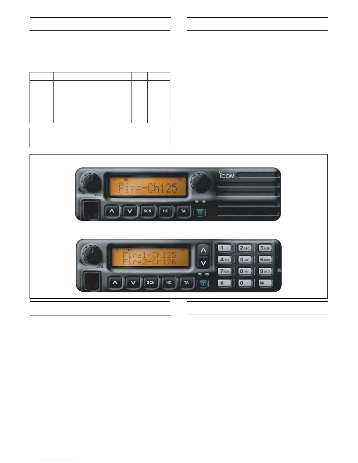
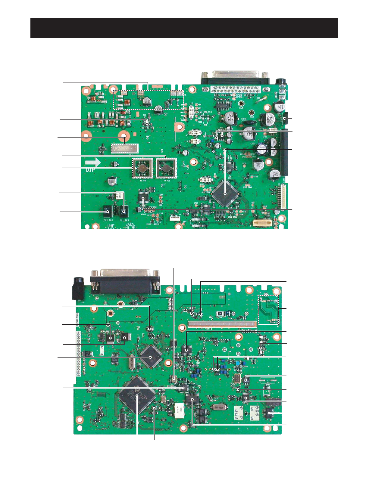
Icom IC-F2721 User manual

SERVICE
MANUAL
UHF MOBLE TRANSCEIVERS

INTRODUCTION DANGER
This service manual describes the latest service information
for the IC-F2721/D/F2710/F2821/D/F2810 UHF MOBILE
TRANSCEIVER at the time of publication.
6 versions of the IC-F2721 have been designed. This
service manual covers each version.
IC-F2700 Series
IC-F2800 Series
ORDERING PARTS
Be sure to include the following four points when ordering
replacement parts:
1. 10-digit order numbers
2. Component part number and name
3. Equipment model name and unit name
4. Quantity required
<SAMPLE ORDER>
1130011600 S.IC TA31136FN IC-F2721D MAIN UNIT 5 pieces
8820001210 Screw 2438 screw IC-F2721 Chassis 12 pieces
Addresses are provided on the inside back cover for your
convenience.
NEVER connect the transceiver to an AC outlet or to a DC
power supply that uses more than 16 V. This will ruin the
transceiver.
DO NOT expose the transceiver to rain, snow or any liquids.
DO NOT reverse the polarities of the power supply when
connecting the transceiver.
DO NOT apply an RF signal of more than 20 dBm (100mW)
to the antenna connector. This could damage the trans-
ceiver's front end.
REPAIR NOTES
1. Make sure a problem is internal before disassembling
the transceiver.
2. DO NOT open the transceiver until the transceiver is
disconnected from its power source.
3. DO NOT force any of the variable components. Turn
them slowly and smoothly.
4. DO NOT short any circuits or electronic parts. An
insulated turning tool MUST be used for all adjustments.
5. DO NOT keep power ON for a long time when the
transceiver is defective.
6. DO NOT transmit power into a signal generator or a
sweep generator.
7. ALWAYS connect a 40 dB to 50 dB attenuator between
the transceiver and a deviation meter or spectrum
analyzer when using such test equipment.
8. READ the instructions of test equipment thoroughly
before connecting equipment to the transceiver.
To upgrade quality, any electrical or mechanical parts and
internal circuits are subject to change without notice or
obligation.
MODEL
IC-F2721D
IC-F2721
IC-F2710
IC-F2821D
IC-F2821
IC-F2810
VERSION
USA-02, USA-03, USA-04, USA-05
USA-06, USA-07
EUR-02, EUR-03, GEN-02, GEN-03
USA-02, USA-03, USA-04, USA-05
USA-06, USA-07
EUR-02, EUR-03, GEN-02, GEN-03
10 KEY
None
Ye s
TX power
45 W
25 W
45 W
25 W

SECTION 1 SPECIFICATIONS
SECTION 2 INSIDE VIEWS
SECTION 3 DISASSEMBLY INSTRUCTIONS
SECTION 4 CIRCUIT DESCRIPTION
4-1 RECEIVER CIRCUITS . . . . . . . . . . . . . . . . . . . . . . . . . . . . . . . . . . . . . . . . . . . . . . . . 4-1
4-2 TRANSMITTER CIRCUITS . . . . . . . . . . . . . . . . . . . . . . . . . . . . . . . . . . . . . . . . . . . . 4-3
4-3 PLL CIRCUITS . . . . . . . . . . . . . . . . . . . . . . . . . . . . . . . . . . . . . . . . . . . . . . . . . . . . . . 4-4
4-4 POWER SUPPLY CIRCUITS . . . . . . . . . . . . . . . . . . . . . . . . . . . . . . . . . . . . . . . . . . . 4-4
4-5 OTHER CIRCUITS . . . . . . . . . . . . . . . . . . . . . . . . . . . . . . . . . . . . . . . . . . . . . . . . . . . 4-5
4-6 PORT ALLOCATIONS . . . . . . . . . . . . . . . . . . . . . . . . . . . . . . . . . . . . . . . . . . . . . . . . 4-6
SECTION 5 ADJUSTMENT PROCEDURES
5-1 PREPARATION. . . . . . . . . . . . . . . . . . . . . . . . . . . . . . . . . . . . . . . . . . . . . . . . . . . . . . 5-1
5-2 LCD CONTRAST ADJUSTMENT . . . . . . . . . . . . . . . . . . . . . . . . . . . . . . . . . . . . . . . 5-4
5-3 SOFT WARE ADJUSTMENT . . . . . . . . . . . . . . . . . . . . . . . . . . . . . . . . . . . . . . . . . . . 5-5
SECTION 6 PARTS LIST
SECTION 7 MECHANICAL PARTS AND DISASSEMBLY
SECTION 8 SEMI-CONDUCTOR INFORMATION
SECTION 9 BOARD LAYOUTS
9-1 FRONT-A UNIT (for IC-F2700 Series) . . . . . . . . . . . . . . . . . . . . . . . . . . . . . . . . . . . . 9-1
9-2 FRONT-B UNIT (for IC-F2800 Series) . . . . . . . . . . . . . . . . . . . . . . . . . . . . . . . . . . . . 9-3
9-3 MAIN UNIT . . . . . . . . . . . . . . . . . . . . . . . . . . . . . . . . . . . . . . . . . . . . . . . . . . . . . . . . . 9-5
SECTION 10 BLOCK DIAGRAM
SECTION 11 VOLTAGE DIAGRAM
11-1 FRONT-A UNIT (for IC-F2700 Series) . . . . . . . . . . . . . . . . . . . . . . . . . . . . . . . . . . . . 11-1
11-2 FRONT-B UNIT (for IC-F2800 Series) . . . . . . . . . . . . . . . . . . . . . . . . . . . . . . . . . . . . 11-2
11-3 MAIN UNIT . . . . . . . . . . . . . . . . . . . . . . . . . . . . . . . . . . . . . . . . . . . . . . . . . . . . . . . . . 11-3
TABLE OF CONTENTS
Icom, Icom Inc. and logo are registered trademarks of Icom Incorporated (Japan) in the United States, the United
Kingdom, Germany, France, Spain, Russia and/or other countries.

S SECTION 1 SPECIFICATIONS
1 - 1
IC-F2721/D, IC-F2821/D IC-F2710, IC-F2810
USA GEN EUR
GENERAL
Measurement method EIA-152-C/204D or TIA-603 EN 300 086
Frequency coverage [L] : 400.000–470.000 MHz
[H] : 450.000–512.000 MHz
[L] : 400.000–470.000 MHz
[H] : 480.000–520.000 MHz
Type of emission
8K10F1E/8K10F1D*/
11K0F3E/16K0F3E
*IC-F2721D, IC-F2821D only
8K50F3E/16K0F3E 8K50F3E/14K0F3E/
16K0F3E
Number of conventional channels Max. 256 channels
Power supply voltage
(negative ground) 13.6 V DC nominal 13.2 V DC nominal
Current drain (approx.)
TX 14.0 A (at 45 W) 7.0 A (at 25 W)
RX Stand-by : 600 mA
Max. audio: 1200 mA
Frequency error ±2.0 ppm ±1.5 kHz
Operating temperature range –30ºC to +60ºC (–22ºF to +140ºF) –25ºC to +55ºC
Dimensions (proj. not included) 175(W) ×45(H) ×170(D) mm; 67⁄8(W) ×125⁄32(H) ×611⁄16(D) in
Weight (approx.) 1.5 kg; 35⁄16 lb
TRANSMITTER
RF output power (Hi/L2/L1) 45 W/25 W/4.5 W 25 W/10 W/2.5 W
Modulation system Variable reactance frequency modulation
Maximum permissible deviation ±2.5 kHz [Narrow], ±4.0 kHz [Middle], ±5.0 kHz [Wide]
Spurious emissions 75 dB typical 0.25 µW (≤ 1 GHz)
1.0 µW (>1 GHz)
Adjacent channel power 60 dB min. [Narrow], 70 dB min. [Middle]/[Wide]
Audio frequency response +2 dB to −5 dB of 6 dB/octave range
from 300 Hz to 2550 Hz [Narrow]/3000Hz [Middle]/[Wide]
Audio harmonic distortion 3% typical at 1 kHz, 40% deviation
Limiting charact of modulator 70–100% of max. deviation
Microphone connector 8-pin modular (600 Ω)
RECEIVER
Receive system Double conversion superheterodyne system
Intermediate frequencies 1st: 46.35 MHz, 2nd: 450 kHz
Sensitivity (typical) 0.3 µV at 12 dB SINAD –4 dBµV (emf) at 20 dB SINAD
Squelch sensitivity (typical) 0.3 µV –4 dBµV (emf)
Adjacent channel selectivity 60 dB min. (75 dB typical) [Narrow], 70 dB min. (80 dB typical) [Middle]/[Wide]
Spurious response 70 dB min. (80 dB typical)
Intermodulation 70 dB min. (75 dB typical) [Narrow]
70 dB min. (77 dB typical) [Wide] 65 dB min. (70 dB typical)
Audio output power 4 W typical at 10% distortion with a 4 Ωload
22 W typical (BTL) at 10% distortion with a 4 Ωload (D-SUB 25 connector)
External SP connector 2-conductor 3.5 (d) mm (1/8")/4 Ω
All stated specifications are subject to change without notice or obligation.

2 - 1
SECTION 2 INSIDE VIEWS
•
Bottom view
•
MAIN UNIT
Top view
Digital CPU
(IC20:
HD64F2239TE16
for IC-F2721D/
F2821D only)
APC amplifier
(IC37: TA75S01F)
Mixer circuit
(D16: HSB88WSTR,
L22, L23)
Base band IC
(IC2: AK2346)
+5V regulator
(Q31: 2SB1132,
Q32: XP6501)
AF amplifier
(IC38: LA4425A)
RX VCO circuit
TX VCO circuit
Power amplifier
IC29:
RA30H4452M [H-25W]
RA30H4047M [L-25W]
RA55H4047M [L-45W]
RA55H4452M [H-45W]
Ceramic filter
(FI1: CFWLB450KE2A
for wide)
Ceramic filter
(FI2: CFWLB450KGFA
for narrow)
RF amplifier
(Q24: 3SK293)
D/A converter
(IC30: M62334FP)
D/A converter
(IC8: M62364FP)
PLL IC
(IC4: LMX2352TM)
FM IF IC
(IC12: TA31136FN)
DTMF decoder
(IC6: LC73872M)
YGR amplifier
(Q23: 2SC5107)
IF amplifier
(Q6: 2SC4215)
Reference crystal oscillator
(X2: CR-794 15.3 MHz)
APC circuit
VCO switch circuit
(Q17: XP1214,
Q18: DTC144EUA)
Low-pass filter
(IC1: NJM12902V)
A/D converter (IC16: AK4550VT-E2 for IC-F2721D/IC-F2821D only)
Digital DSP
(IC41:
TMS320VC5416PGE120 for IC-F2721D/IC-F2821D only)
MAIN CPU
(IC23: HD64F2268F)
+8V regulator
(IC36: TA7808F)
T8V regulator
(Q34: 2SD1664)
Power switch
(Q42: 2SJ377)
Drive amplifier
(Q48: 2SC3356)

2 - 2
•
FRONT-B UNIT (IC-F2800 Series)
•
FRONT-A UNIT (IC-F2700 Series)
Backlight
dimmer control
ALC amplifier
(IC9: AN6123MS)
Mic amplifier
(IC5: TC75S51F)
LCD driver
(IC7: SED1526F0A)
Reset IC
(IC2: S-80942CNMC)
Mic switch
(IC8: TC4W53F)
Q3: 2SC4116
Q4: DTC114TU
Q5: DTC114TU
Front CPU
(IC3: HD64F3687)
Mic switch
(IC8: TC4W53F)
ALC amplifier
(IC9: AN6123MS)
Backlight
dimmer control
Q3: 2SC4116
Q4: DTC114TU
Q5: DTC114TU
Front CPU
(IC3: HD64F3687)

3 - 1
SECTION 3 DISASSEMBLY INSTRUCTIONS
•REMOVING THE FRONT UNIT
1 Unscrew 4 screws, A, then remove the bottom cover.
w Unplug J1(B) and J6 (C).
3 Unscrew 2 screws, D.
4 Remove the front unit in the direction of the arrow.
• REMOVING THE MAIN UNIT
1 Remove the bushing, L.
wRemove the MAIN unit in the direction of the arrow.
J1 *
A
B
C
D
D
L
E
F
•BEFORE REMOVING THE MAIN UNIT
1 Unscrew 8 screws, Eand remove the shield plate F.
G
H
I
J
K
2 Unscrew 4 screws, Gand remove the shield cover H.
3 Unsolder 3 points, Iand 5 points J.
4Remove 2 clips, K.
Continue to right above

4 - 1
• 2ND IF DEMODULATOR CIRCUIT
SECTION 4 CIRCUIT DESCRIPTION
FI1
2nd IF filter
450 kHz
Noise
detector
Q1
Limiter
amp.
Quadrature
detector
Active
filter
AF signals
5V
Q3
IF
AMP
X4 Discriminator
IC8
Mixer
X2
15.3 MHz
45.9 MHz
1st IF from the IF amplifier (Q6)
“NOIS” signal to the CPU (IC23)
“DFIL” signal to the digital IF filter (FI3)
8
2
1
75
BPF
32
3
161311109
IC12
TA31136FN
Noise
amp.
Noise
comparator
FI2
4-1 RECEIVER CIRCUITS
4-1-1 ANTENNA SWITCHING CIRCUIT (MAIN UNIT)
The antenna switching circuit functions as a low-pass filter
while receiving and a resonator circuit while transmitting.
This circuit does not allow transmit signals to enter the
receiver circuits.
Received signals enter the antenna connector (CHASSIS;
J1) and pass through the low-pass filters (L42–L44, L49
C376, C388, C389, C391, C432, C461, C551, C552). The
filtered signals are passed through the λ⁄4type antenna
switching circuit (D29–D31).
While receiving, no voltage is applied to the D29–D31. Thus,
the receive line and ground are disconnected and L39, C384
function as a low-pass filter which leads received signals to
the RF circuits via the limiter (D27, D28).
4-1-2 RF CIRCUIT (MAIN UNIT)
The RF circuit amplifies signals within the range of frequen-
cy coverage and filters out-of-band signals.
The signals from the antenna switching circuit pass through
the two-stage tunable bandpass filters (D23, D26, D68,
D69, L32, L36). The filtered signals are amplified at the RF
amplifier (Q24) and then passed through the another two-
stage tunable bandpass filters (D17, D18, L28) to suppress
unwanted signals. The filtered signals are applied to the 1st
mixer circuit.
D17, D18, D23, D26, D68 and D69 employ varactor diodes,
that are controlled by the Main CPU (IC23) via the D/A
converter (IC30, pins 1, 2) to track the bandpass filter.
These varactor diodes tune the center frequency of an RF
passband for wide bandwidth receiving and good image
response rejection.
4-1-3 1ST MIXER AND 1ST IF CIRCUITS (MAIN UNIT)
The 1st mixer circuit converts the received signals into fixed
frequency of the 1st IF signal with the PLL output frequency.
By changing the PLL frequency, only the desired frequency
passes through a monolithic filter at the next stage of the
1st mixer.
The RF signals from the bandpass filter are mixed with
the 1st LO signal, where come from the RX VCO circuit
(RX VCO1: Q11, D7, D11; RX VCO2: Q12, D9, D13) via
the 1st LO amplifier (Q21) and low-pass filter (L24, L26,
C246, C264, C516) at the 1st mixer circuit (D16, L22, L23)
to produce a 46.35 MHz 1st IF signal. The 1st IF signal is
amplified at IF amplifiers (Q10, Q13, Q14), and then passed
through a monolithic filter (FI4) to suppress unwanted sig-
nals and to pass only the desired signals.
The filtered signal is applied to the IF amplifier (Q6) and
then applied to the 2nd IF circuit.
4-1-4 2ND IF AND DEMODULATOR CIRCUITS
(MAIN UNIT)
The 2nd mixer circuit converts the 1st IF signal into a 2nd
IF signal. The double conversion superheterodyne system
(which convert receive signals twice) improves the image
rejection ratio and obtains stable receiver gain.
The 1st IF signal from the IF amplifier (Q6) is applied to
the 2nd mixer section of the FM IF IC (IC12, pin 16), and
is mixed with the 2nd LO signal to be converted into a
450 kHz 2nd IF signal.
The FM IF IC (IC12) contains the 2nd mixer, limiter ampli-
fier, quadrature detector, active filter and noise amplifier
circuits.

4 - 2
Base band IC
(IC2)
Base band IC
(IC2)
AF signal
from FM IF IC (IC12, pin 9)
23 20 AF
AMP
IC38
Speaker
IC5
IC43 IC42
IC1 IC8 D12
Microphone
AMP
MIC ALC
3
7
4
FM/PM switch
D/A converter FM mod.
LPF
"CTCSS/DTCS" signal from
D/A conveter (IC8, pin 10)
"TONE" signal from
D/A converter (IC8, pin 22)
to TX VCO circuit
(Q12, D70, D71)
3
AMP
IC34
FRONT UNIT A/B
3
5
4
IC42
15 341 4
IC8
16
3
5
3
4
1
2
15
IC43
6
7
1
IC8
IC9
AMP
2
12
13
14
1
15
IC42
• AF AND MIC AMPLIFIER CIRCUIT
A 2nd LO signal (45.9 MHz) is produced at the PLL circuit
by tripling it’s reference frequency (X2: 15.3 MHz).
The 2nd IF signal from the 2nd mixer section (IC12, pin 3)
passes through the ceramic filter(s) (Wide: FI1 only, Narrow:
both FI1 and Fl2) to remove unwanted heterodyned frequen-
cies. It is then amplified at the limiter amplifier section (IC12,
pin 5) and applied to the quadrature detector section (IC12,
pins 10, 11) to demodulate the 2nd IF signal into AF signals.
The demodulated AF signals are output from pin 9 (IC12)
and applied to the base band IC (IC2).
4-1-5 AF AMPLIFIER CIRCUIT (MAIN UNIT)
The AF amplifier circuit amplifies the demodulated AF sig-
nals to drive a speaker. This transceiver employs the base
band IC which is composed of pre-amplifier, expander,
scrambler, MSK de-modulator, etc. at the AF amplifier sec-
tion.
The AF signals from the FM IF IC (IC12, pin 9) are passed
through the DIG/ANA switch (IC42, pins 2, 15) and are then
applied to the base band IC (IC2, pin, 23). The signals are
amplified at the AF amplifier section in the base band IC (IC2,
pin 23), and are then applied to the high-pass and low-pass
filter sections of it.
The signals pass through the high-pass filter to suppress
unwanted harmonic components. The filtered signals pass
through (or bypass) scrambler and expander sections. The
signals are amplified at the amplifier section in the base
band IC (IC2).
The output signals from the base band IC (IC2, pin 20) are
passed through the RX/PA switch (IC43, pins 1, 15) and
DIG/ANA switch (IC42, pins 3, 4). The signals are applied
to the AF volume (IC8, pins 15, 16), and are then applied to
the AF amplifiers (IC34, IC38).
The power amplified AF signals are applied to the internal
speaker (IC-F2700 series only) that is connected to J6 via
[EXT SP] jack (J5).
4-1-6 SQUELCH CIRCUITS (MAIN UNIT)
• NOISE SQUELCH
A squelch circuit cuts out AF signals when no RF signals
are received. By detecting noise components in the AF sig-
nals, the squelch circuit switches the AF amplifier controller.
Some noise components in the AF signals from the FM IF
IC (IC12, pin 9) are passed through the D/A converter (IC8,
pins 1, 2). The signals are applied to the active filter section
in the FM IF IC (IC12, pin 8). The active filter section filters
and amplifies noise components. The amplified signals are
converted into the pulse-type signals at the noise detector
section. The detected signals output from pin 13 (NOIS) via
the noise comparator section.
The “NOIS” signal from the FM IF IC is applied to the Main
CPU (IC23, pin 37). Then the Main CPU analyzes the noise
condition and outputs the AF mute signal as “AFON” from
the pin 19 to the AF power controller (Q28, Q29, D34, D36).
• CTCSS AND DTCS
The tone squelch circuit detects tone signals and opens the
squelch only when receiving a signal containing a matching
subaudible tone (CTCSS or DTCS). When tone squelch is in
use, and a signal with a mismatched or no subaudible tone
is received, the tone squelch circuit mutes the AF signals
even when noise squelch is open.
A portion of the AF signals from the FM IF IC (IC12, pin 9)
pass through the low-pass filter (Q54) to remove AF (voice)
signals, and are then applied to the amplifier (Q54). The
amplified signals are applied to the CTCSS or DTCS decod-
er in the Main CPU (IC23, pin 46) via the “CDEC” line. The
Main CPU outputs the AF mute signal as “AFON” from the
pin 19 to the AF power controller (Q28, Q29, D34, D36).

4 - 3
POWER
AMP.
APC
AMP.
DRIVE
AMP.
+
1
3
4
–
HV
to antenna
connector
T2
TMUT
RF signal
from PLL circuit
T8V
APC control circuit
FOR
REV
Q48
Q23
IC37
IC29
D40D38
YGR
AMP.
• APC CIRCUIT
4-2 TRANSMITTER CIRCUITS
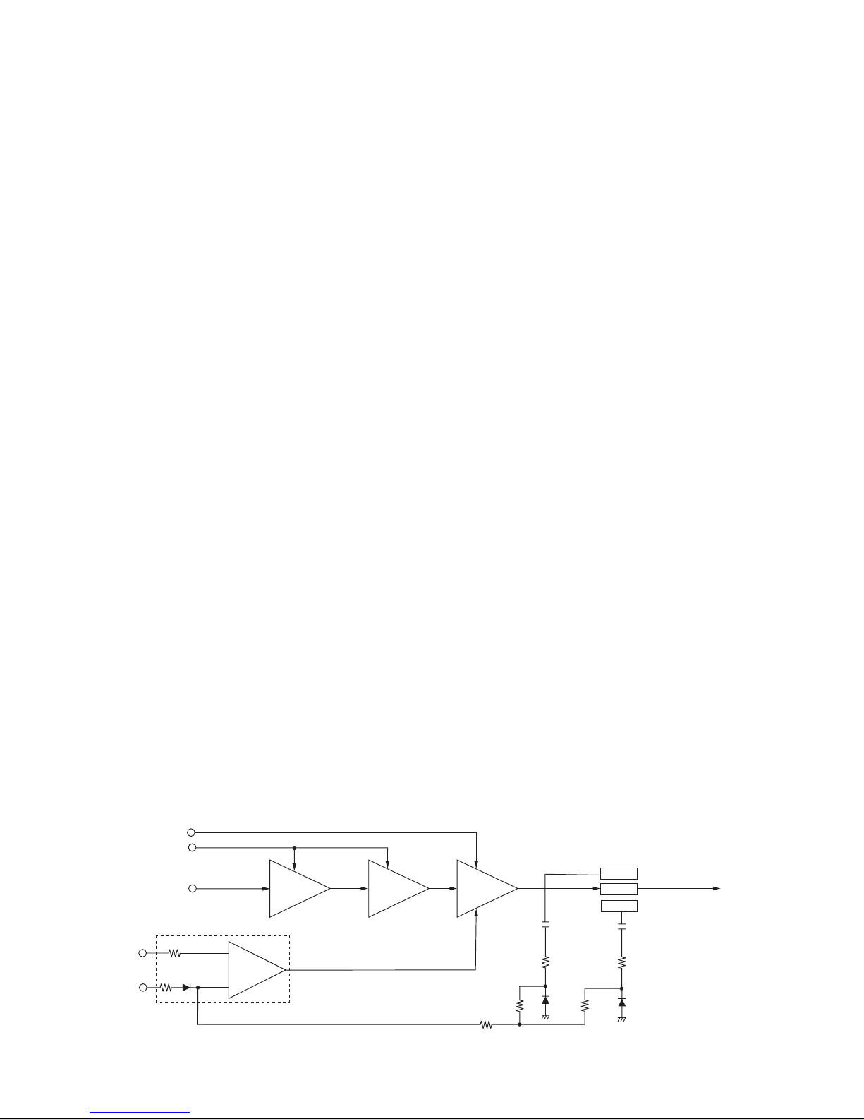
4-2-1 MICROPHONE AMPLIFIER CIRCUIT (MAIN UNIT)
The microphone amplifier circuit amplifies audio signals
within +6 dB/octave pre-emphasis 6 characteristics from the
microphone to a level needed for the modulation circuit.
This transceiver employs the base band IC which is com-
posed of microphone amplifier, compressor, scrambler,
limiter, splatter filter, MSK modulator, etc. at the microphone
amplifier section.
The AF signals from the microphone connector (FRONT
UNIT; J2, pin 6) are passed through the microphone switch
(FRONT UNIT; IC8, pins 1, 6, 7) and are then applied to the
ALC amplifier (FRONT UNIT; IC9) during digital mode oper-
ation (bypassed during FM mode operation.) The signals are
amplified at the microphone amplifier (FRONT UNIT; IC5,
pins 3, 4) and then applied to MAIN UNIT via J1 (pin 10).
The amplified signals are applied to the microphone ampli-
fier section of the base band IC (IC2, pin 3). The amplified
signals are passed through (or bypass) the compressor,
scrambler sections of IC2, and are then passed through the
high-pass, limiter amplifier, splatter filter sections of IC2.
The output signals from the base band IC (IC2, pin 7) are
applied to the FM/PM switch (IC43, pins 12–14) after pass
through the microphone switch (IC42, pins 12, 14). The sig-
nal are passed through the low-pass filter (IC1, pins 4, 13)
and then applied to the D/A converter (IC8, pins 3, 4). The
output signal from D/A converter (IC8, pin 3) are applied to
the modulation circuit (D12).
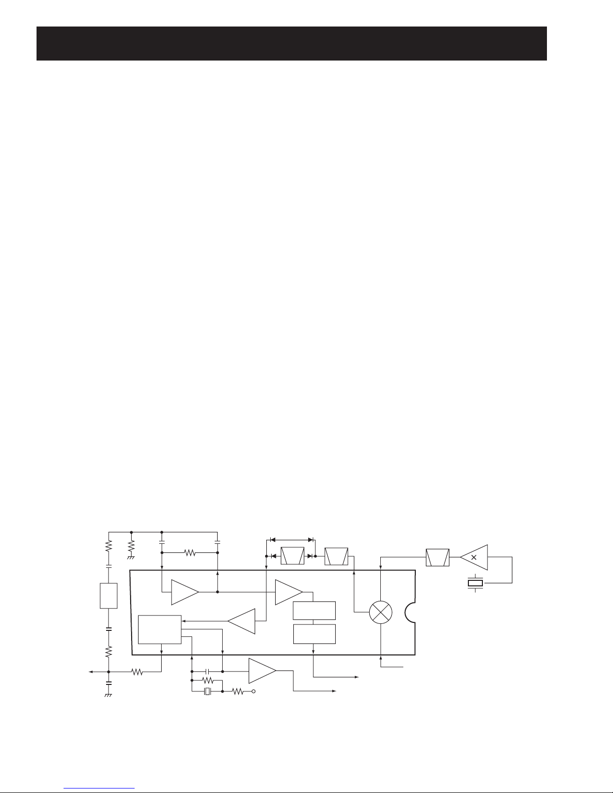
4-2-2 MODULATION CIRCUIT (MAIN UNIT)
The modulation circuit modulates the VCO oscillating signal
(RF signal) using the microphone audio signals.
The AF signals from the D/A converter (IC8, pin 3) change
the reactance of varactor diode (D12) to modulate the oscil-
lated signal at the TX VCO circuit (Q16, D70 D71). The
modulated VCO signal is amplified at the buffer amplifiers
(Q20, Q22) and is then applied to the YGR (Q23) amplifier
via the T/R switch (D19).
The CTCSS/DTCS signals (“CENC0”, “CENC1”, ”CENC2”)
from the Main CPU (IC23, pins 89–91) are combined at
resistors (R158, R159, R162) and are then pass through the
low-pass filter (IC9, pins 12, 14).
The filtered signals are applied to the D/A converter (IC8,
pins 9, 10), and are then mixed with the filtered microphone
audio signals. The mixed signals are applied to the D/A con-
verter (IC8, pin 3, 4) after pass through the low-pass filter
(IC1, pins 8, 9). The output signal from D/A converter (IC8,
pin 3) are applied to the D12 in the TX VCO circuit.
4-2-3 POWER AMPLIFIER CIRCUITS (MAIN UNIT)
The power amplifier circuits amplify the VCO oscillating sig-
nal to an output power level.
The signal from the T/R switch (D19) is amplified at the YGR
(Q23), drive (Q48) and power (IC29) amplifiers to obtain 45
W (IC-F2721/D/F2821/D; 25 W for IC-F2710/F2810) of RF
power.
The amplified signal is passed through the low-pass filter
(L35, C345, C346, C348, C349), antenna switch (D29, D30),
low-pass filters (L42–L44, C376, C388, C389, C391, C551,
C552), power detector (D38, D40) and low-pass filter (L49,
C432, C461), and is then applied to the antenna connector
(CHASSIS unit; J1).
The bias voltage of the power amplifier (IC29) is controlled
by the APC circuit.
4-2-4 APC CIRCUIT (MAIN UNIT)
The APC circuit protects the power amplifier from a mis-
matched output load and stabilizes the output power.
The power detector circuit (D38, D40) detects the forward
signals and reflection signals and converts it into DC volt-
age. The output voltage is at a minimum level when the
antenna impedance is matched with 50 Ωand is increased
when it is mismatched.
The detected voltage is applied to the differential amplifier
(IC37; pins 3, 4), and the “T2” signal from the D/A converter
(IC30, pin 2), controlled by the main CPU (IC23), is applied
to the other input for reference (IC37, pin 1). When antenna
impedance is mismatched, the detected voltage exceeds the
power setting voltage. Then the output voltage of the differ-
ential amplifier (IC37, pin 4) controls the bias voltage of the
power amplifier (IC29) to reduce the output power.

• PLL CIRCUIT
4 - 4
4-3 PLL CIRCUITS
4-3-1 PLL CIRCUIT (MAIN UNIT)
A PLL circuit provides stable oscillation of the transmit fre-
quency and receive 1st LO frequency. The PLL output com-
pares the phase of the divided VCO frequency to the refer-
ence frequency. The PLL output frequency is controlled by
the divided ratio (N-data) of a programmable divider.
The PLL circuit contains the RX VCO1 (Q11, D7, D11), RX
VCO2 (Q12, D9, D13) and TX VCO (Q16, D70, D71). The
oscillated signal is amplified at the buffer amplifier (Q20).
The output signal is applied to the buffer amplifier (Q19),
and is then applied to the PLL IC (IC4, pin 6).
The PLL IC contains a prescaler, programmable counter,
programmable divider and phase detector, etc. The applied
signal is divided at the prescaler and programmable counter
section by the N-data ratio from the main CPU (IC23). The
divided signal is detected on phase at the phase detector
using the reference frequency and output from pin 4. The
output signal is passed through the loop filter (Q46, Q47,
Q50) and is then applied to the VCO circuit.
If the oscillated signal drifts, its phase changes from that of
the reference frequency, causing a lock voltage change to
compensate for the drift in the oscillated frequency.
4-3-2 VCO CIRCUITS (MAIN UNIT)
The VCO circuits contains a separate RX VCO1 (Q11, D9,
D13), RX VCO2 (Q12, D9, D13) and TX VCO (Q16, D70,
D71). The oscillated signal is amplified at the buffer ampli-
fiers (Q20, Q22) and is then applied to the T/R switch (D19,
D20). Then the receive 1st LO (Rx) signal is applied to the
1st mixer (L22, L23, D16) and the transmit (Tx) signal to the
YGR amplifier circuit (Q23).
Loop
filter
PLST
SSO
SCK
4
Q12, D9, D13
RX VCO2
Q11, D7, D11
RX VCO1
TX VCO
Q16 D70, D71
6
10
14
15
16 PLL control signals from CPU (IC23)
15.3 MHz reference signal
from reference frequency osciilator (X2)
IC4 LMX2352TM
Shift register
Prescaler
Phase
detector
Programmable
counter
Programable
divider
Buffer
Q20
Buffer
Q22
Buffer
Q19
to transmitter circuit
to 1st mixer circuit
D19
D20
LPF
4-4 POWER SUPPLY CIRCUITS
Line Description
HV The voltage from a DC power supply.
VCC
The same voltage as the HV line which is
controlled by the power switch circuit (Q41,
Q42). When the [ ] is pushed, the Main
CPU (IC23)outputs the "PWR" control signal
to the power switch circuit to turn the circuit
ON.
CPU 5
Common 5 V converted from the HV line
at the CPU 5 regulator circuit (IC40). The
output voltage is applied to the Main CPU
(IC23) and EEPROM
(IC26), etc.
5V
Common 5 V converted from the CPU 5 line
at the 5 V regulator circuit (Q31, Q32). The
output voltage is applied to the PLL IC (IC4)
and D/A converter IC (IC8), etc.
8V
Common 8 V converted from the VCC line
at the 8 V regulator circuit (IC36). The output
voltage is applied to the buffer amplifier (Q22)
and AF amplifier (IC34), etc.
T8V
Transmit 8 V controlled by the T8V regulator
circuit (Q34) using the "TMUT" signal from
the Main CPU (IC23). The output voltage is
applied to the YGR (Q23) and driver (Q48)
amplifiers, etc.
R8V
Receive 8 V controlled by the R8V regulator
circuit (Q30) using the "TXC" signal from
the Main CPU (IC23). The output voltage is
applied to the RF amplifier (Q24) and 1st IF
amplifier (Q6), etc.
• VCO FREQUECY LIST
[L-band] [H-band]
RX VCO1 400.00–434.995 MHz 450.00–484.995 MHz
RX VCO2 435.00–470.00 MHz 485.00–520.00 MHz
TX VCO 400.00–470.00 MHz 450.00–520.00 MHz
A portion of the signal from the buffer amplifier (Q20) is fed
back to the PLL IC (IC4, pin 6) via the buffer amplifier (Q19)
as the comparison signal.

4 - 5
Scrambler/
De-scrambler
TX/RX
HPF
Pre-
emphasis Limiter Splatter VR2
Expander VR4
RXA2
SMF
De-
emphasis
Com-
pressor
VR1
(HPF)
RX
LPF
VR3
(HPF)
7 MOD
18
19
20 SIGNAL
3TXIN
23RXIN
21SDEC
10
14MDIR
9
MTDT
MTCK
13MSCK
11MDIO
12MRDF
MSK
Modulator
MSK
Demodulator
MSK
BPF
Control
Register
TXA1
RXA1
• DIGITAL MODE CIRCUIT
BPF
From FM IF IC
(IC12) To AF amplifier circuit
From
MIC amplifier
(FRONT UNIT; IC15)
To FM/PM SW
(IC43)
AMP AMP
AMP
Q3
IC42
RECEIVED SIGNAL
FI3 IC15 IC16
IC41
IC18
IC18IC13 IC44
IC42
IC2
A/D LINER
CODEC
IC
LINER
CODEC
IC
BASE
BAND
IC
DIG/ANA
SW
DSP
IC
MIC SW LPF
TRANSMIT SIGNAL
4-5 OTHER CIRCUITS
4-5-1 COMPANDER CIRCUIT (MAIN UNIT)
IC-F2700/2800 series have compander circuit which can
improve S/N ratio and become wide dynamic range. The
circuit is composed in the base band IC (IC2).
(1) WHILE RECEIVING
The demodulated AF signals from the FM IF IC (IC12, pin
9) are applied to the amplifier section in base band IC (IC2,
pin 23), and then pass through the low-pass and high-pass
filter section to suppress unwanted signals. The filtered
signals pass through (or bypass) scrambler section, and are
then applied to the expander circuit to expand AF signals.
The output signals from the base band IC (IC2, pin20)
is applied to the AF amplifier circuit after amplified at the
amplifier section.
(2) WHILE TRANSMITTING
The audio signals from the microphone are applied to the
base band IC (IC2, pin 3) via microphone amplifier (FRONT
UNIT; IC5). The signals are amplified at the amplifier section,
and are then applied to the compressor circuit to compress
the audio signals. The signals pass through (or bypass)
scrambler section, and are then applied to the limiter section
after being passed through the high-pass filter.
The filtered signals pass through the splatter filter section,
and are then applied to the modulation circuit (D12) via the
FM/PM switch (IC43, pins12–14) and D/A converter (IC8,
pins 2, 3).
4-5-2 DIGITAL MODE CIRCUIT (IC-F2721D/F2821D only)
(1) WHILE RECEIVING
A portion of the 2nd IF signal from the limiter amplifier sec-
tion in the FM IF IC (IC12) output from pin 11 and is ap-
plied to the IF amplifier (Q3). The amplified signal is passed
through a ceramic bandpass filter (FI3) to suppress hetero-
dyne noise, and amplified again at the digital IF amplifier
(IC15, pins, 1, 4). The amplified 2nd IF signal is applied to
the A/D converter (IC16) to be converted into digital IF sig-
nal, then applied to the DSP IC (IC41). The DSP IC converts
the digital IF signal into the digital audio signal.
The digital audio signal from DSP IC are converted into ana-
log audio signals at the LINER CODEC IC (IC18) and output
from pin 16.
The audio signals are applied to the base band IC (IC2,
pin 23) after being pass through the DIG/ANA switch (IC42,
pins 1, 15).
(2) WHILE TRANSMITTING
The microphone signal from the base band IC (IC2, pin 7)
are amplified at the MOD amplifier (IC44, pins 3, 4) and are
then applied to the LINER CODEC IC (IC18, pin 2) to con-
vert into the digital audio signal.
The digital audio signal is processed by DSP IC (IC41), and
applied to the LINER CODEC IC (IC18) again.
The signal from the LINER CODEC IC (IC18, pin 15) is
passed through the low-pass filter (IC13, pins 1, 3, 6, 7) and
then applied to the PM/FM switch (IC43, pins 12–14) after
pass through the microphone switch (IC42 pins 13, 14).
• BASE BAND IC DIAGRAM (IC2: AK2346-E2)

4 - 6
4-6 PORT ALLOCATIONS
4-6-1 Main CPU (MAIN UNIT; IC23)
Pin
number
Port
name Description
1 DSDA I/O port for data signal to the D/A con-
verter (IC30 pin 6).
2 DAST Outputs strobe signals to the D/A con-
verter (IC8, pin 6).
10 SSO Outputs serial data to the PLL IC (IC4,
pin 15) and D/A converter (IC8, pin 8).
11 SCK
Outputs clock signal to the PLL IC (IC4
pin 14), D/A converter (IC8, pin 7),
etc.
13 PLST Outputs strobe signals to the PLL IC
(IC4, pin 16).
15 DASW
Outputs control signal to the digital
/analog switch (IC42).
Low: While analog mode is se-
lected.
16 TXC
Outputs the T8V regulator circuit (Q34)
control signal.
Low: During transmit.
17 TMUT
Outputs the R8V regulator circuit
(Q30) control signal.
Low: During receive.
18 AFON
Outputs control signal for AF mute cir-
cuit (Q28, Q29).
High: While AF amplifier (IC38) is
activated.
19 NWC
Outputs wide/narrow switch (D2, D4)
control signal.
High: When narrow band is se-
lected.
20 DDSD Input port for serial data from the
DTMF decoder IC (IC6, pin 9).
21 DDAC Outputs clock signals to the DTMF
decoder IC (IC6, pin 10).
32 RMUT
Input port for the AF mute signal from
the optional unit via J2.
Low: While RX audio is muted.
33 MMUT
Input port for the microphone mute
signal from the optional unit via J2.
Low: While microphone audio is
muted.
34–36 OPT1–
OPT3 I/O ports for optional unit.
37 NOIS Input port for the noise signal from the
FM IF IC (IC9, pin 13).
38 POSW Input port for the [ ] switch.
Low: While [ ] switch is pushed.
39 DDST
Input port for DTMF detection sig-
nal from the DTMF decoder IC (IC6,
pin 11).
40 IGSW Input port for the remote power control
signal from external connector, J7.
41 PWON
Outputs control signal for the power
switch circuit (Q41, Q42).
Low: While power ON.
43 SENC Outputs single tone encoder signal.
Pin
number
Port
name Description
44 BEEP Outputs beep audio signals.
45 SDEC
Input port for single tone decode
signal from the base band IC (IC2,
pin 21).
46 CDEC Input port for CTCSS/DTCS signal
from the LPF (IC1, pin 7).
47 ULCK Input port for the PLL unlock signal.
Low: The PLL circuit is unlocked.
48 BATV Input port for the connected battery
for the low battery detection.
49 LVIN Input port for the PLL lock voltage.
50 RSSI Input port for the S-meter signal from
the FM IF IC (IC12, pin 12).
51 TEMP Input port for the transceiver’s internal
temperature detecting signal.
68 CLO Outputs the data signal to the FRONT
CPU (FRONT UNIT; IC3).
69 CLI Input port for the data signal from the
FRONT CPU (FRONT UNIT; IC3).
72 HORN
Outputs external device control signal.
High: When matched 5/2 tone sig-
nals are received.
78 MTCK
Input port for transmitting MSK clock
signal from the base band IC (IC2,
pin 9).
79 NTXD
Outputs NMEA data signals for the
connected unit via external connector
(J7).
80 NRXD
Input port for NMEA data signals from
the connected unit via external con-
nector (J7).
88 DIM
Input port for the LCD backlight con-
trol signal from the external connector
(J8).
Low: While LCD backlight is
dimmed.
89–91 CENC0–
CENC2 Output the CTCSS/DTCS signals.
93 MTDT Outputs the MSK data to the base
band IC (IC2, pin 10).
94 MDIR Outputs serial data control signal to
the base band IC (IC2, pin 14 ).
95 MDIO
I/O port for the serial data signals
from/to the base band IC (IC2,
pin 11).
96 MSCK Outputs clock signal for the base band
IC (IC2, pin 13).
97 PMFM
Outputs the FM/PM switch (IC43,
pin 11) control signal.
High: While PM is selected.
98 ESDA I/O port for data signals from/to the
EEPROM (IC26, pin 5).
99 ESCL Outputs clock signal to the EEPROM
(IC26, pin 6).

4 - 7
4-6-2 FRONT CPU (FRONT UNIT; IC3)
Pin
number
Port
name Description
7 RES Input port for rest signal.
19–22 KR0–
KR3
Input ports for the 10-keypad.
(IC-F2800 series only)
28, 29 LIGT1,
LIGT2
Output control signals for LCD back-
light.
47 LEDT Outputs control signal for the TX LED.
48 LEDR Outputs control signal for the RX LED.
51, 52 DICK,
DIUP
Input ports for control signal from the
dial (S9). (IC-F2700 series only)
53, 54 KYUP,
KYDN
Input ports for control signal from [ ],
[ ] keys. (IC-F2800 series only)
57 HANG
Input port for the microphone hanger
detection signal.
Low: While microphone on the
hanger.
58 PTT Input port for the PTT switch of the
connected microphone.
59–63 KYP0–
KYP4
Input ports for the programmable
function keys (P0–P4).
4-6-4 D/A CONVERTER (MAIN UNIT; IC30)
Pin
number
Port
name Description
1T1
Outputs the bandpass filters (D23,
D26, D68, D69) tuning signal.
2T2
• While receiving
Outputs the bandpass filters (D17,
D18) tuning signal.
• While transmitting
Outputs the TX power control signal
which selects TX output power of
HIGH, LOW1 or LOW2. The output
signal is applied to the APC amplifier
(IC37, pin 1).
3 TXLVA Outputs TX VCO lock voltage.
4 RXLVA Outputs RX VCO lock voltage.
4-6-3 D/A CONVERTER (MAIN UNIT; IC8)
Pin
number
Port
name Description
2 SQL Outputs AF signal to the squelch cir-
cuit (IC12, pin 8).
3 MOD Outputs modulation signals to the
VCO circuit.
10 TENC Outputs CTCSS/DTCS signals.
11 BAL Outputs deviation balance control sig-
nal.
14 BEPV
Outputs beep audio signals to the
speaker via the AF amplifiers (IC34,
IC38).
15 SIGNAL Outputs AF signals to the speaker via
the AF amplifiers (IC34, IC38).
22 TONE Outputs single tone signal.
23 REF Outputs reference oscillator (X2) con-
trol signal.
LIGT1 LIGT2 LIGHT
HIGH HIGH DIM
HIGH LOW OFF
LOW HIGH ON
LOW LOW OFF

SECTION 5 ADJUSTMENT PROCEDURES
5 - 1
▄ REQUIRED TEST EQUIPMENT
EQUIPMENT GRADE AND RANGE EQUIPMENT GRADE AND RANGE
DC power supply Output voltage
Current capacity
: 13.6 (13.2) V DC
: 20 A or more Audio generator Frequency range
Measuring range
: 300–3000 Hz
: 1–500 mV
Modulation analyzer Frequency range
Measuring range
: DC–600 MHz
: 0 to ±10 kHz Attenuator Power attenuation
Capacity
: 50 or 60 dB
: 100 W
Frequency counter
Frequency range
Frequency accuracy
Sensitivity
: 0.1–600 MHz
: ±1 ppm or better
: 100 mV or better
Standard signal
generator (SSG)
Frequency range
Output level
: 0.1–600 MHz
: 0.1 µV to 32 mV
(–127 to –17 dBm)
Digital multimeter Input impedance : 10 MΩ/V DC or more AC millivoltmeter Measuring range : 10 mV to 10 V
RF power meter
Measuring range
Frequency range
Impedance
SWR
: 1–75 W
: 100–800 MHz
: 50 Ω
: Better than 1.2 : 1
Oscilloscope Frequency rang
Measuring range
: DC–20 MHz
: 0.01–20 V
External speaker Input impedance
Capacity
: 4 Ω
: 10 W or more
5-1 PREPARATION
When adjusting IC-F2721/D,F2710,F2821/D,F2810, the optional CS-F70/F1700 ADJ ADJUSTMENT SOFTWARE (Rev. 1.0 or later)
and JIG CABLE (modified OPC-1122 CLONING CABLE; see illustration on page 5-3) are required.
▄SYSTEM REQUIREMENTS
• Microsoft®Windows®98/98SE/Me/2000/XP
• RS-232C serial port (D-sub 9 pin)
▄ ADJUSTMENT SOFTWARE INSTALLATION
qQuit all applications when Windows is running.
wInsert the CD into the appropriate CD drive.
eDouble-click the “Setup.exe” contained in the adjustment
software folder in the CD drive.
rThe “Welcome to the InstallShield Wizard for adjustment
software will appear. Click [Next>].
tThe “Choose Destination Location” will appear. Then click
[Next>] to install the software to the destination folder.
y
After the installation is completed, the “InstallShield Wiz-
ard Complete” will appear. Then click [Finish].
uEject the CD.
iThe adjustment software icon appears on the desk top
screen.
▄ BEFORE STARTING SOFTWARE ADJUSTMENT
Program the adjustment frequencies into the transceiver
using with the cloning software before starting the software
adjustment. Otherwise, the transceiver can not start software
adjustment.
CAUTION!: BACK UP the originally programmed mem-
ory data in the transceiver before program-
ming the adjustment frequencies.
When program the adjustment frequencies into
the transceiver, the transceiver’s memory data
will be overwritten and lose original memory
data at the same time.
Microsoft and Windows are registered trademarks of
Microsoft Corporation in the U.S.A. and other countries.
▄STARTING SOFTWARE ADJUSTMENT
qConnect the transceiver and PC with JIG CABLE.
wTurn the transceiver power ON.
eBoot up Windows, and click the adjustment software icon
on the screen.
rClick ‘Connect’ on the adjustment software window, then
appears transceiver’s adjustment screen.
tSet or modify adjustment data as desired.
• ADJUSTMENT FREQUENCY LIST
CH FREQUENCY CONDITIONS
1400.000 MHz [L]
450.000 MHz [H]
TX power
Mode
: Low1
: Wide
2400.000 MHz [L]
450.000 MHz [H]
TX power
Mode
: Low1
: Narrow
3400.000 MHz [L]
450.000 MHz [H]
TX power
Mode
: Low1
: Digital
4400.000 MHz [L]
485.000 MHz [H]
TX power
Mode
CTCSS
: Low1
: Wide
: 151.4 Hz
5415.000 MHz [L]
485.000 MHz [H]
TX power
Mode
: Low1
: Wide
6415.000 MHz [L]
485.000 MHz [H]
TX power
Mode
: Low1
: Narrow
7415.000 MHz [L]
485.000 MHz [H]
TX power
Mode
: Low1
: Digital
8435.000 MHz [L]
485.000 MHz [H]
TX power
Mode
: Low1
: Wide
9435.000 MHz [L]
485.000 MHz [H]
TX power
Mode
: Low2
: Wide
10 435.000 MHz [L]
485.000 MHz [H]
TX power
Mode
: High
: Wide
11 435.000 MHz [L]
485.000 MHz [H]
TX power
Mode
: Low1
: Narrow
12 470.000 MHz [L]
520.000 MHz [H]
TX power
Mode
: Low1
: Wide
13 470.000 MHz [L]
520.000 MHz [H]
TX power
Mode
: Low1
: Narrow
14 470.000 MHz [L]
520.000 MHz [H]
TX power
Mode
: Low1
: Digital

5 - 2
r
t
y
e
u
q
w
i
!0
!2
!5
!6
!7
o
!8
!9
@1
@0
@2 @3
!1
!3
!4
q: Reloads adjustment data
w: Transceiver's connection state
e: Connected DC voltage measurement
r: PLL lock voltage measurement
t: RF output power
y: FM modulation balance
u: FM modulation preset
i: CTCSS/DTCS deviation
o: Squelch level
!0: Reference frequency
!1: Receive sensitivity (automatic)
!2: Receive sensitivity (manual)
!3: PLL lock voltage preset for RX (automatic)
!4: PLL lock voltage preset for TX (automatic)
!5: S-meter (FM)
!6: S-meter (digital)
!7: Deviation (narrow)
!8: Deviation (wide)
!9: Deviation (digital)
@0: DSP reference frequency
@1: Base band center voltage
@2: Digital mode
@3: 2/5 TONE, DTMF deviation
NOTE: The above values for settings are example only.
Each transceiver has its own specific values for each setting.
• CS-F70/F1700 ADJ'S SCREEN EXAMPLE

5 - 3
Modulation analyzer
(DC measurable)
Attenuator
50 dB or 60 dB
to the antenna connector
to DC cable
Standard signal generator
–127 to –17 dBm
(0.1 V to 32 mV)
CAUTION:
DO NOT transmit while
SSG is connected to
the antenna connector.
RF power meter
50 Ω/ 1–75 W
DC power supply
13.6 (13.2) V / 20 A
Frequency
counter
PC
to the MIC
connector
to an RS-232C port
JIG CABLE
RS-232C cable
(straight)
IC-F2721/D
IC-F2821/D
IC-F2710
IC-F2810
[]
AC millivoltmeter
Audio generator
+Audio generator
300 Hz to 3 kHz
AC
millivoltmeter
MICE
MIC
PTT
PTT switch
PTTE
Add a jumper wire here
Electrolytic
capacitor
47µF
OPC-1122
(Cloning cable)
• CONNECTION
• JIG CABLE

5 - 4
5-2 LCD CONTRAST ADJUSTMENT
ADJUSTMENT ADJUSTMENT CONDITION MEASUREMENT VALUE ADJUSTMENT
UNIT LOCATION UNIT ADJUST
LCD
CONTRAST
1 • Operating CH. : CH 1 FRONT A/B Connect a digital
multimeter or an oscillo-
scope to the check point
"CONTRAST".
–2.0 V FRONT A/B R59
• Preset LCD contrast
: 64
(user set mode)
• Receiving
• FRONT-A UNIT for IC-F2700 series
• FRONT-B UNIT for IC-F2800 series
LCD CONTRAST CHECK POINT
R59: LCD CONTRAST ADJUSTMENT
LCD CONTRAST CHECK POINT
R59: LCD CONTRAST ADJUSTMENT

5 - 5
5-3 SOFT WARE ADJUSTMENT
Select an operation using [↑] / [↓] keys, then set specified value using [←] / [→] keys on the connected computer keyboard.
ADJUSTMENT ADJUSTMENT CONDITION MEASUREMENT VALUE
UNIT LOCATION
PLL LOCK
VOLTAGE
[LV (RX LVA1)]
[LV (RX LVA2)]
[LV (TX LVA)]
1 • Operating CH. : CH 1
• Preset LV(RX1) : 34 [0.67 V]
• Receiving
PC
screen
Check the "LVIN" item on the
CS-F70/F1700 ADJ's screen.
0.67 V
2 • Operating CH. : CH 8
• Preset LV(RX2) : 34 [0.67 V]
• Receiving
0.67 V
3 • Operating CH. : CH 1
• Preset LV(TX) : 51 [1.00 V] [L]
34 [0.67 V] [H]
• Transmitting
1.00 V [L]
0.67 V [H]
CONVENIENT:
The PLL lock voltage can be adjustment automatically.
Set the cursor to "RX LVA"/"TX LVA" and then push [ENTER] key.
REFERENCE
FREQUENCY
[REF]
1 • Operating CH. : CH 12
• Connect an RF power meter or 50 Ω
dummy load to the antenna connector.
• Transmitting
Rear
panel
Loosely couple a frequency
counter to the antenna connec-
tor.
470.0000 MHz [L]
520.0000 MHz [H]
DSP
FREQUENCY
[Dig REF]
(IC-F2721D/
F2821D only)
1 • Operating CH. : CH 14
• Connect an RF power meter or 50 Ω
dummy load to the antenna connector.
• Transmitting
MAIN
unit
Connect a frequency counter to
CP19.
12.288000 MHz
BASE BAND
FREQUENCY
[Dig DA]
(IC-F2721D/
F2821D only)
1 • Operating CH. : CH 14
• Preset Dig Mode : 13
• Connect an RF power meter or 50 Ω
dummy load to the antenna connector.
• Transmitting
Rear
panel
Loosely couple a frequency
counter to the antenna connec-
tor.
470.0000 MHz [L]
520.0000 MHz [H]
CP19: DSP frequency
check point
• MAIN UNIT

5 - 6
SOFTWARE ADJUSTMENT (Continued)
Select an operation using [↑] / [↓] keys, then set specified value using [←] / [→] keys on the connected computer keyboard.
ADJUSTMENT ADJUSTMENT CONDITION MEASUREMENT VALUE
UNIT LOCATION
OUTPUT
POWER
[Power (Hi)]
1 • Operating CH. : CH 10
• Transmitting
Rear
panel
Connect an RF power meter to
the antenna connector.
25.0 W [25W]
45.0 W [45W]
[Power (L2)] 2 • Operating CH. : CH 9
• Transmitting
10.0 W [25W]
25.0 W [45W]
[Power (L1)] 3 • Operating CH. : CH 8
• Transmitting
2.5 W [25W]
4.5 W [45W]
MODULATION
BALANCE
[BAL]
1 • Operating CH. : CH 11
• Preset [MOD N] : 100
• No audio applied to the [MIC] connector.
• Set a modulation analyzer as:
HPF : OFF
LPF : 20 kHz
De-emphasis : OFF
Detector : (P–P)/2
• Push [P0] while transmitting.
Rear
panel
Connect a modulation analyzer
with an oscilloscope to the
antenna connector through an
attenuator.
Set to square wave
form
FM
DEVIATION
(NARROW)
[MOD N C]
1• Operating CH. : CH 6
• Connect an audio generator to the [MIC]
connector and set as
: 1.0 kHz/40 mVrms
• Set a Modulation analyzer as:
HPF : OFF
LPF : 20 kHz
De-emphasis : OFF
Detector : (P–P)/2
• Transmitting
Rear
panel
Connect a modulation ana-
lyzer to the antenna connector
through an attenuator.
±2.10 kHz
(NARROW)
[MOD N L]
2• Operating CH. : CH 2
• Transmitting
(NARROW)
[MOD N H]
3• Operating CH. : CH 13
• Transmitting
(WIDE)
[MOD W C]
4• Operating CH. : CH 5
• Transmitting
±4.10 kHz
(WIDE)
[MOD W L]
5• Operating CH. : CH 1
• Transmitting
(WIDE)
[MOD W H]
6• Operating CH. : CH 12
• Transmitting
(MIDDLE)
[MOD W C]
([EUR] only)
7• Operating CH. : CH 5
• Transmitting
±3.20 kHz
(MIDDLE)
[MOD W L]
([EUR] only)
8• Operating CH. : CH 1
• Transmitting
(MIDDLE)
[MOD W H]
([EUR] only)
9• Operating CH. : CH 12
• Transmitting
This manual suits for next models
5
Table of contents
Other Icom Transceiver manuals