Icop VDX-6300RD User manual

VDX-6300RD
VSX-6100-EVB (Evaluation board)
DM&P Vortex86DX 800MHz
DIP 68pin CPU Module
with (3x TX/ RX only)/2USB/LAN/2GPIO/CF/PWMx24
256MB DDR2 Onboard
User’s Manual
(Revision 1.1A)

Copyright
The information in this manual is subject to change without notice for continuous improvement in
the product. All rights are reserved. The manufacturer assumes no responsibility for any
inaccuracies that may be contained in this document and makes no commitment to update or to
keep current the information contained in this manual.
No part of this manual may be reproduced, copied, translated or transmitted, in whole or in part,
in any form or by any means without the prior written permission of the IC P Technology Inc..
Copyright 2008 IC P Technology Inc.
Manual No. IUM6100-EVB000-01 Ver.1.0A May, 2008
Manual No. IUM6300D000-01 Ver.1.0A March, 2011
Manual No. IUM6300RD000-01 Ver.1.1A September, 2014
Trademarks Acknowledgment
Vortex86DX is the registered trademark of IC P Technology Inc.
ther brand names or product names appearing in this document are the properties
and registered trademarks of their respective owners. All names mentioned herewith
are served for identification purpose only.

T a b l e o f C o n t e n t s
T a b l e o f C o n t e n t s ............................................................. iii
C h a p t e r 1 Introduction……………………………………………1
1.1 Packing List ............................................................ 1
1.2 Product Description ................................................ 1
1.3 Specifications ......................................................... 3
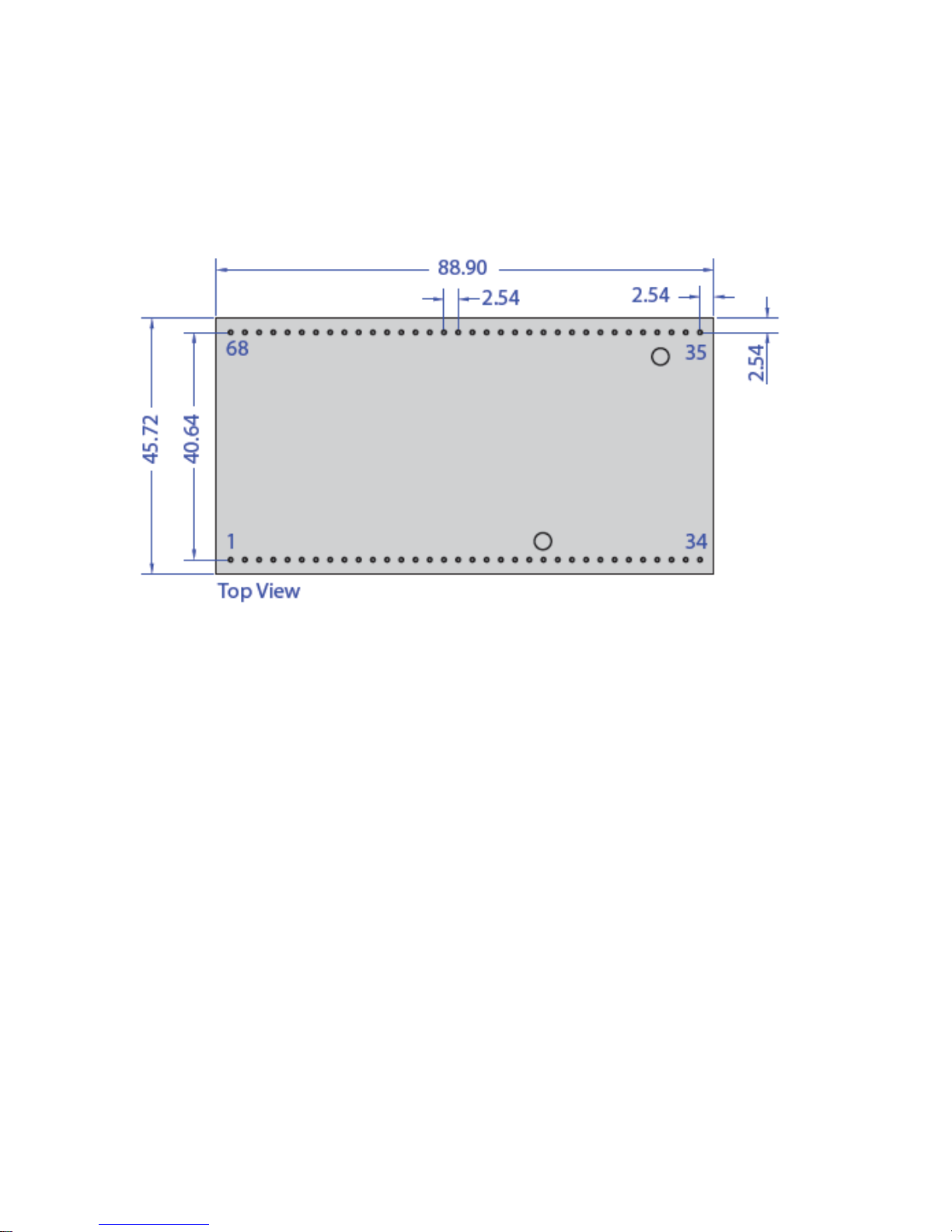
1.4 Board Dimension .................................................... 5
C h a p t e r 2 Installation……………………………………………..7
2.1 Board utline ......................................................... 7
2.2 Connectors & Jumpers Location .................... ........8
2.3 Connectors & Jumpers Summary ......................... 10
2.4 Pin Assignments & Jumper Settings ..................... 12
2.5 System Mapping ................................................... 20
2.6 Watchdog Timer ................................................... 23
2.7 GPI .................................................................... 24
2.8 SPI flash ............................................................... 25
2.9 PWM .................................................................... 26
C h a p t e r 3 Driver Installation……………………………………27
Appendix ………………………………………………………………..28
A. TCP/IP library for D S real mode ............................. 28
B. BI S Default Setting ................................................. 29
C. Console redirection Setting ....................................... 30
D. VSX-6100-EVB Schematic ........................................ 35
Warranty ............................................................................................ 36

This page is blank

VDX-6300RD Vortex86DX DIP 68pin CPU Module
1
C h a p t e r 1
Introduction
1.1 Packing List
Product Name Package
VDX-6300RD
Embedded Vortex86DX DIP 68 Pin PU Module
RS232 cable x 3
USB cable x 1
PS/2 Keyboard cable x 1
Product Name Package
VSX-6100-EVB
Embedded Vortex86SX/DX DIP 68pin PU
Module Evaluation board x 1
Manual & Drivers D x 1
Note:
All cables will be included only, when you order the whole set of
VDX-6300RD and VSX-6100-EVB.

VDX-6300RD Vortex86DX DIP 68pin CPU Module
2
1.2 Product Description
The VDX-6300RD family of low-power x86 embedded controller is designed to meet DIP 68pin
CPU module specification, and integrated with the following features.
800MHz Vortex86DX System- n-Chip
256MB DDR2 system memory
10/100Mbps Ethernet
3 USB 2.0 (host)
Up to 3 serial ports
16-bit GPI x2
2 watchdog timer
PWM 16~24 channels
JTAG interface
AMI BI S
nboard 4MB SPI Flash
DC IN: +6V~+24V
Support extended operating
temperature range of -20°C to +70°C
The VDX-6300RD DIP 68pin controller is designed with backward compatibility in mind, to
provide migration path for projects facing end-of-life challenges with their existing x86 based
controller. The VDX-6300RD family of controller is designed as a plug in replacement, with
backward compatibility to support legacy software to help extend existing product life cycle
without heavy re-engineering.
VDX-6300RD is suitable for broad range of data-acquisition, Industrial automation, Process
control, Automotive controller, AVL, Intelligent Vehicle management devic,Medical device,
Human machine interface, Robotics, machinery control And more…application that required
small footprint, low-power and low-cost hardware with open industry standard such as DIP 68pin
module.

VDX-6300RD Vortex86DX DIP 68pin CPU Module
3
1.3 Specifications
Features VSX-6100-EVB (Evaluation board)
Connectors
2.00mm ∅10-pin header for RS-232 x1
2.54mm ∅10-pin header for PWM x1
2.54mm ∅10-pin header for GPIO x3
2.54mm ∅3-pin header for SERVO x8
2.54mm ∅34-pin connector for Multi-I/O x1
External USB connector x2
External RJ-45 connector for Ethernet x1
External 9-pin D-Sub male connector for RS-232 x1
Power Requirement
+6V~+24V
@
250mA
Dimension
101mm X 78mm (3.97 x3.07 inches)
76
76g
perating
Temperature
-20
o
C ~ +70
o
C
-40°C ~ +85°C (Optional)

VDX-6300RD Vortex86DX DIP 68pin CPU Module
4
Features VDX-6300RD
CPU
DM&P SoC CPU Vortex86DX- 800MHz
Real Time Clock with Lithium Battery Backup
Cache
L1:16K I-Cache, 16K D-Cache L2:128KB Cache
BI S
AMI BIOS
System Memory
256 /512MB DDR2 Onboard
Watchdog Timer
Software programmable from 30.5 us to 512 seconds x2
sets(Watchdog 1 fully compatible with M6117D)
I / Interface
RS-232 port x3
USB port x1 (USB 2.0 version)
Connectors
1.25mm ∅3-pin Wafer for RS-232 x3
1.25mm ∅4-pin Wafer for USB x1
1.25mm ∅4-pin Wafer for KBD x1
1.25mm ∅6-pin Wafer for JTAG x1
Type I/II Compact Flash slot x1
Flash Disk Support
Onboard 4MB SPI Flash Disk (Driver: A)
Type I/II CF Card
Power Requirement
Single Voltage +5V
@
380mA
Dimension
90mm X 46mm (3.54 x1.81 inches)
Weight
30g
perating
Temperature
-20
o
C ~ +70
o
C
-40°C ~ +85°C (Optional)

VDX-6300RD Vortex86DX DIP 68pin CPU Module
5
1.4 Board Dimension
VSX-6100-EVB (Evaluation board)

VDX-6300RD Vortex86DX DIP 68pin CPU Module
6
VDX-6300RD

VDX-6300RD Vortex86DX DIP 68pin CPU Module
7
C h a p t e r 2
Installation
2.1 Board Outline
VDX-6300RD

VDX-6300RD Vortex86DX DIP 68pin CPU Module
8
2.2 Connectors & Jumpers Location
VSX-6100-EVB (Evaluation board)

VDX-6300RD Vortex86DX DIP 68pin CPU Module
9
VDX-6300RD

VDX-6300RD Vortex86DX DIP 68pin CPU Module
10
2.3 Connectors & Jumpers Summary
VSX-6100-EVB (Evaluation board)
Summary Table
Nbr Description Type of onnections
Pin
nbrs.
J1 10/100Base-T Ethernet LAN RJ45 Connector 8-pin
J2 GPI Port 0 / 1 Pin Header, 2.54∅ ,10x2
20-pin
J3 USB 2 USB connector 6-pin
J4 Timer Counter C M2 Pin Header, 2.54∅ ,10x2
20-pin
J5 USB 1 USB connector 6-pin
J6 SERV 1 Pin Header, 2.54∅, 3x1 3-pin
J7 RS232 / TTL select (C M1) Pin Header, 2,54∅,1x2 2-pin
J8 SERV 2 Pin Header, 2.54∅, 3x1 3-pin
J9 SERV 3 Pin Header, 2.54∅, 3x1 3-pin
J10 C M1 Pin Header, 2.0∅ 5x2 10-pin
J11 SERV 4 Pin Header, 2.54∅, 3x1 3-pin
J12 System Power connector
(DC IN: +6V~+24V)
Terminal Block 5.0∅,2x1 2-pin
J13 SERV 5 Pin Header, 2.54∅, 3x1 3-pin
J14 C M1 D-Sub Male 9-pin
J15 SERV 6 Pin Header, 2.54∅, 3x1 3-pin
J16 SERV 7 Pin Header, 2.54∅, 3x1 3-pin
J17 SERV Power connector Terminal Block 5.0∅,2x1 2-pin
J18 SERV 8 Pin Header, 2.54∅, 3x1 3-pin
J19 IRQ6 select Pin Header, 2,54∅,1x2 2-pin
U1 DIP-68 Connector Box Header, 2.54∅ 34x2 68-pin
SW1 RESET SWITCH
SP1 BUZZER

VDX-6300RD Vortex86DX DIP 68pin CPU Module
11
VDX-6300RD
Summary Table
Nbr Description Type of onnections
Pin
nbrs.
J2 USB Wafer, 1.25∅ , 5x1 5-pin
J3 PS/2 Keyboard Wafer, 1.25∅ , 5x1 4-pin
J4 JTAG Wafer, 1.25∅ , 6x1 6-pin
J5 C M3 Wafer, 1.25∅ , 3x1 3-pin
J6 C M4 Wafer, 1.25∅ , 3x1 3-pin
J8 Console Redirection Slide Switch 3-pin
J9 C M9 Wafer, 1.25∅ , 3x1 3-pin
U5 DIP-68 Connector Pin Header, 2.54∅ 34x2 68-pin
F1 Compact Flash Type I/II CF Connector 50-pin
PWR-LED
Power Active LED (Red) LED-SMD
IDE- LED
IDE Active LED (Green ) LED-SMD
LED 3
LAN Link/Active LED (Green)
LED-SMD
LED 4
LAN Duplex LED ( Yellow ) LED-SMD

VDX-6300RD Vortex86DX DIP 68pin CPU Module
12
2.4 Pin Assignments & Jumper Settings
A: Pin Assignments & Jumper Settings of VSX-6100-EVB
J2: GPIO (Port 0 / Port 1)
J4: Timer ounter ( OM2)
Pin # Signal Name
Pin #
Signal Name
1 GND 2 VCC
3 GP00 4 GP10
5 GP01 6 GP11
7 GP02 8 GP12
9 GP03 10
GP13
11 GP04 12
GP14
13 GP05 14
GP15
15 GP06 16
GP16
17 GP07 18
GP17
19 VCC 20
GND
Pin # Signal Name
Pin #
Signal Name
1 GND 2 VCC
3 UT0 4 GP30
5 UT1 6 GP31
7 UT2 8 GP32
9 CLK0 10
GP33
11 CLK1 12
GP34
13 CLK2 14
GP35
15 GATE0 16
GP36
17 GATE1 18
GP37
19 GATE2 20
GND

VDX-6300RD Vortex86DX DIP 68pin CPU Module
13
J6: SERVO1
Pin # Signal Name
1
GND
2
VDD
3
P20
J7:RS232 / TTL select ( OM1)
Pin # Signal Name
PEN C M1 RS232
CL SE C M1 TTL / Port4
J8: SERVO2
Pin # Signal Name
1
GND
2
VDD
3
P21
J9: SERVO3
Pin # Signal Name
1
GND
2
VDD
3
P22

VDX-6300RD Vortex86DX DIP 68pin CPU Module
14
J10: OM 1
Pin # Signal
Name
Pin # Signal
Name
1 DCD1
2 RXD1
3 TXD1
4 DTR1
5 GND 6 DSR1
7 RTS1
8 CTS1
9 RI1 10 GND
11 GND
J11: SERVO4
Pin # Signal Name
1
GND
2
VDD
3
P23
J12: System Power onnector (Terminal Block 5.0mm)
Pin # Signal Name
1
DC IN :
+
6V~
+
24V
2
GND
J13: SERVO5
Pin # Signal Name
1
GND
2
VDD
3
P24
J15: SERVO6
Pin # Signal Name
1
GND
2
VDD
3
P25

VDX-6300RD Vortex86DX DIP 68pin CPU Module
15
J16: SERVO7
Pin # Signal Name
1
GND
2
VDD
3
P2
6
J17: SERVO Power onnector (Terminal Block 5.0mm)
Pin # Signal Name
1
VDD
2
GND
J18: SERVO8
Pin # Signal Name
1
GND
2
VDD
3
P2
7
J19: IRQ6 selection
Pin # Signal Name
1
GND
2
IRQ6

VDX-6300RD Vortex86DX DIP 68pin CPU Module
16
U1: DIP-68 onnector – 68pin
Pin # Signal Name Pin #
Signal Name
1
GND
35
GND
2
Reset
36
TXDEN2
3
GP00
/PWM0
37
CTS2
\
4
GP01
/PWM1
38
D
S
R
2
\
5
GP02
/PWM2
39
DTR
2
\
6
GP03
/PWM3
40
RXD2
\
7
GP04
/PWM4
41
RI
2
8
GP05
/PWM5
42
RTS2
9
GP06
/PWM6
43
TXD2
10
GP07
/PWM7
44
DCD2
\
11
SPICS/ GP30
45
GND
12
SPICLIK
/ GP31
46
GP23
/PWM19
13
SPID
/ GP32
47
GP24
/PWM20
14
SPIDI
/ GP33
4
8
GP25
/PWM21
15
GP34
49
GP26
/PWM22
16
GP35
50
GP27
/PWM23
17
GP3
6
51
CTS1 / GP47
18
GP3
7
52
DSR1 / GP46
19
SPEAKER
53
DTR1 / GP45
20
GP20
/PWM16
54
RXD1 / GP44
21
GP2
1
/PWM17
55
RI1 / GP43
22
GP2
2
/PWM18
56
RTS1 / GP42
23
VBATT
57
TXD1 / GP4
1
24
VCC
58
DCD1 / GP40
25
GP10
/PWM8
59
GND
26
GP11
/PWM9
60
LUSBD0
-
27
GP12
/PWM10
61
LUSBD0+
28
GP13
/PWM11
62
LUSBD1
-
29
GP14
/PWM12
63
LUSBD1+
30
GP15
/PWM13
64
LAN
-
RX
-
3
1
GP16
/PWM14
65
LAN
-
RX+
32
GP17
/PWM15
66
LAN
-
TX
-
33
SYSCLK
67
LAN
-
TX+
34
IRQ6
68
VCC
Note:
1. Multi-function pins of U1 are controlled by BIOS setting.
2. If you Enable 4M SPI flash Disk in BIOS setting, you cannot use GP30~GP33 Pins.
This manual suits for next models
1
Table of contents
Other Icop Motherboard manuals

Icop
Icop VDX-6318 User manual

Icop
Icop VEX2-6427 User manual

Icop
Icop VDX-6328RD-NF User manual

Icop
Icop NAD11-103-SD User manual

Icop
Icop athena User manual

Icop
Icop VORTEX86-6047LV-6S User manual

Icop
Icop VEX-6225 User manual

Icop
Icop VSX-6121-FD-V2 Series User manual

Icop
Icop VSX-6124-V2 User manual

Icop
Icop VSX-6121-V2 User manual