IDT VersaClock 3S User manual
1©2017 Integrated Device Technology, Inc. June 8, 2017
Introduction
The evaluation board is designed to help the customer evaluate the 5P35023 device, the latest addition to the family of programmable
devices in IDT's Timing portfolio. When the board is connected to a PC running IDT Timing Commander™ software through a USB, the
device can be configured and programmed to generate different combinations of frequencies.
Board Overview
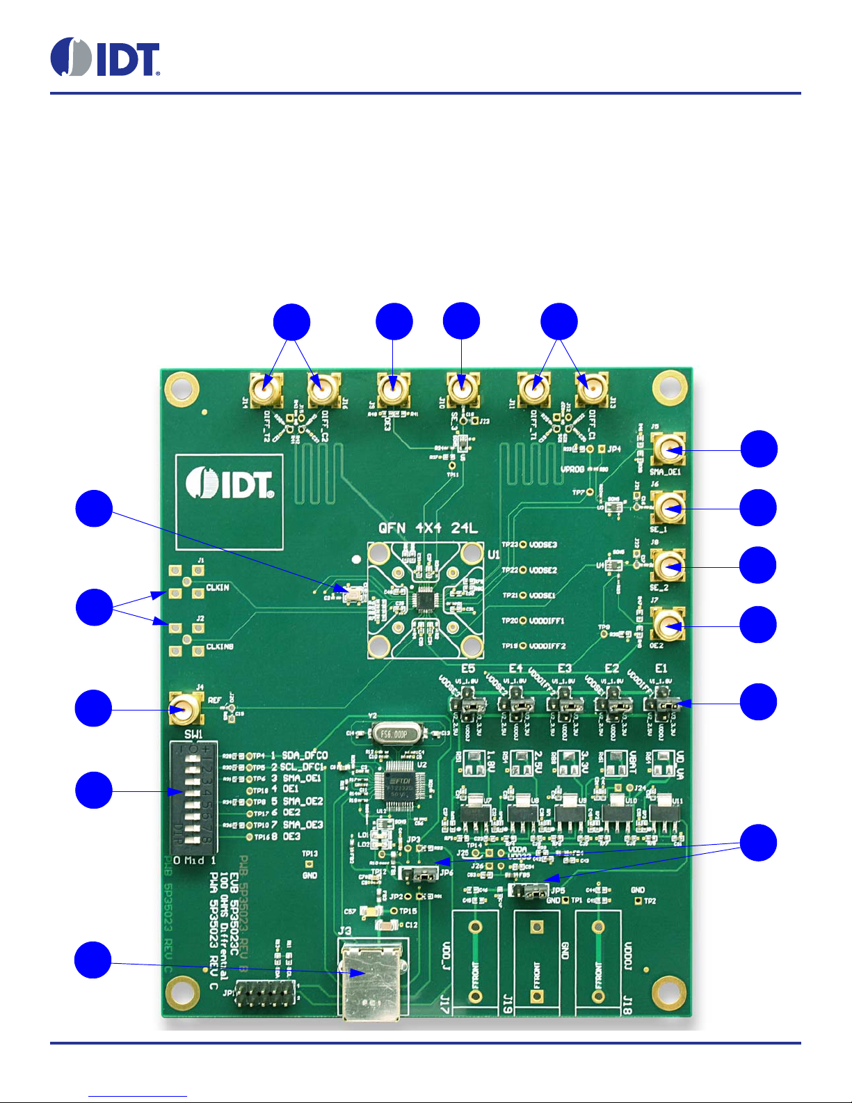
Use Figure 1 and Table 1 to identify: USB connector and the input and output frequency SMA connectors.
Figure 1. EVK5P35023 Evaluation Board
4
3
2
1
5
J
I
G
F
E
D
C
B
A
H
User Manual
VersaClock®3S - 5P35023 Evaluation Board
2©2017 Integrated Device Technology, Inc. June 8, 2017
VersaClock®3S - 5P35023 Evaluation Board User Manual
Board Power Supply
Power Supply Options
The core voltage includes a digital voltage VDD33 and an analog voltage VDDA. Both core voltages can be powered by USB as default.
▪USB Power Supply only – When the board is connected to a PC through a USB cable, on-board voltage regulators will generate a
3.3V for the device. In this case, place the jumper as shown in Figure 2. See the JP5 jumper position for the on-board voltage
regulators in the following figure. USB power source is recommended because it's readily available right from your laptop.
Table 1. Evaluation Board Labels and Functions
Label
Number Name On-boardConnector
Label Function
1 DIP Switch SW1 This is used to set outputs enable/disable on the IC and switches DFC
in different configurations.
2 Reference Output REF This is the reference or buffered output from the crystal.
3
Differential Clock Input CLKIN/CLKINB A differential clock can be connected as source for the device.
Single-ended Clock Input CLKINB A Single-ended clock can be connected as source for the device using
CLKINB only.
4 Crystal, 25MHz This crystal is used as a reference source for the clock signal.
5 USB Connector J3 Connect this USB to your PC to run IDT Timing Commander.
A Differential Output #2 DIFF_T2/C2 This can be a differential pair, or two single-ended outputs. By default,
it’s an LPHCSL differential output.
B Output-enable Connector OE3 This port can be used in Pro-active Power Saving (PPS) mode.
C Single-ended Output SE_3 This is the single-ended output. By default it’s an LVCMOS
single-ended output.
D Differential Output #1 DIFF_T1/C1 This can be a differential pair, or two single-ended outputs. By default,
it’s LPHCSL differential output.
E Output-enable Connector SMA_OE1 This port can be used in Pro-active Power Saving (PPS) mode.
F Single-ended Output SE_1 This is the single-ended output. By default it’s an LVCMOS
single-ended output.
G Single-ended Output SE_2 This is the single-ended output. By default it’s an LVCMOS
single-ended output.
H Output enable Connector OE2 This port can be used in Pro-active Power Saving (PPS) mode.
I Output Voltage Selector E1, E2, E3, E4, E5 This is a four-way header used to select an output voltage. Connect
center pin to GND, and then the respective voltage (3.3V as default).
J Input Selector JP5, JP6 This is used to configure input from USB or external power supply.

3©2017 Integrated Device Technology, Inc. June 8, 2017
VersaClock®3S - 5P35023 Evaluation Board User Manual
Figure 2. JP5 Jumper Position (pins 1 & 2) for the On-Board Voltage Regulators
Jumping to the pin configuration as shown will select the power source from on-board voltage regulators powered by USB.
Output Clock Voltages
Like VDDA and VDD33 having two sources, each output voltage is also provided with two sources to choose from: bench power supply or
powered from USB. The selection is made by a 4-way header as shown in Figure 3 below.
The jumper can be used to select a voltage for E1, E2, E3, E4, and E5 respectively. The on-board voltage regulators powered by USB are
1.8V, 2.5V and 3.3V; VDDOJ is from bench power supply connecting to JP17 and JP18
Note: Each output voltage can be individually selected. Use the label on the evaluation board: E1 for VDDDIFF1, E2 for VDDSE1, E3 for
VDDDIFF2, E4 for VDDSE2 and E5 for VDDSE3.
Figure 3. Jumper Configuration for On-board Voltage Regulators
Connecting the Board
The board is connected to a PC through a USB connector for configuring and programming the device, as shown in Figure 4 below. The
USB interface will also provide +5V power supply to the board, from which on-board voltage regulators generate various voltages for the
core as well as for each output.
Note: The USB port only supports USB 2.0; USB 3.0 is not supported at this time.

4©2017 Integrated Device Technology, Inc. June 8, 2017
VersaClock®3S - 5P35023 Evaluation Board User Manual
Figure 4. Connecting the Board with USB Port for Communications with Timing Commander Software
On-board Crystal
A 25MHz crystal is installed on the board and is used as a source for reference frequency.
Board Default Frequency Output
Table 2. Board Default Frequency Output
Serial Output Output Frequency
1 SE_1 (Single-ended) —
2 SE_2 (Single-ended) 48MHz
3 SE_3 (Single-ended) 60MHz
4 REF (Single-ended: Reference output) 25MHz
5 DIFF_T1/C1 (Differential output) 100MHz
6 DIFF_T2/C2 (Differential output) 100MHz
5©2017 Integrated Device Technology, Inc. June 8, 2017
VersaClock®3S - 5P35023 Evaluation Board User Manual
DIP Switch (SW1)
Configuration and Setup from I2C Port
Table 3. DIP Switch (SW1)
Serial DIP Switch Pin Number DIP Switch Pin Name State Mode
A 1 SDA_DFCO Floating/Tri-state —
B 2 SCL_DFC1 Floating/Tri-state Software I2C
C 3, 5, 7 SMA_OE1, SMA_OE2, SMA_OE3 High or 1 —
D 4, 6, 8 OE1, OE2, OE3 High or 1 —
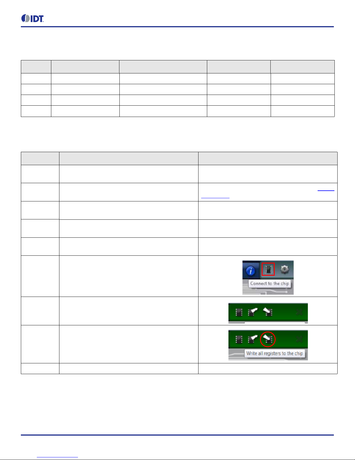
Table 4. Configuration and Setup from I2C Port
Step Number Step Description Comments
1 Set SCL_OFC1 Pin (DIP switch pin 2). High or 1. The default setting from the board is pull-high
internally.
2 Launch 5P35023 Timing Commander software. Refer to 5P35023 Timing Commander User Guide, Timing
Commander software.
3Follow the “Getting Started Steps” in Timing Commander
software.
An I2C connection is established between GUI software
and VersaClock 3S device.
4Using the Timing Commander GUI, start a new settings
file, or open a pre-optimized file.
Configure the Timing Commander software for the
required sets of outputs.
5 Connect J3 to a USB Port using the supplied I2C cable. An I2C connection is established between GUI software
and VersaClock 3S chip.
6Connect to the EVB by clicking on the microchip icon
located at the right of the Timing Commander.
7
Once configured, new options will be available on a green
background indicating that the EVB has successfully
connected with the board.
8Write the setting to the device by clicking on the write all
registers to the chip option.
9 All intended outputs should be available for measurement. —

6©2017 Integrated Device Technology, Inc. June 8, 2017
VersaClock®3S - 5P35023 Evaluation Board User Manual
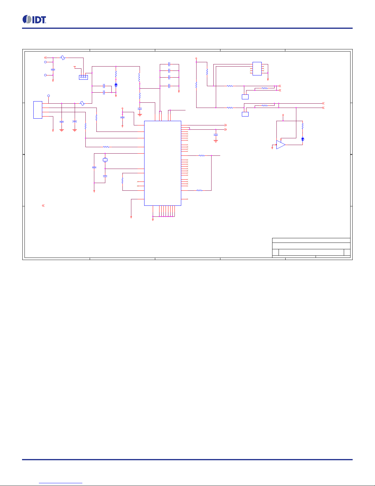
Evaluation Board Schematics
Evaluation board schematics are shown on the following pages.
Figure 5. Evaluation Board Schematic (1)
5
5
4
4
3
3
2
2
1
1
D D
C C
B B
A A
Layout notes.
2.Do not share crystal load
3.Route power from bead through
4.Do not share ground vias. One
ground pin one ground via.
1.Separate Xout and Xin traces
by at least 3 x the trace width.
other components.
capacitor ground via with
then to clock chip Vdd pad.
through 0.1uF capacitor pad
bulk capacitor pad then
grounded but is not required.
5.Exposed pad should be Locate near U1.6
Locate near DUT
power pin
CLKINB
CLKIN
SCL_DFC1
SDA_DFC0
SER1
SER2
SER3
SE_1
SE_2
SE_3
OE1
OE2
OE3
SER4 SE_4
SE_[4:1]
CLKIN
CLKINB
GND
CLKIN_CONN
CLKINB_CONN
CLKIN
CLKINB
OE[3:1]
OE3
OE2
DIFFRT1
DIFFRC1
DIFFRC2
DIFFRT2
OE1
DIFF_T1
DIFF_C1
DIFF_C2
DIFF_T2
DIFF_T[2:1]
DIFF_C[2:1]
DIFF_T[2:1]
DIFF_C[2:1]
VDDSE2
VDDSE3
Node#3
VDDA_VDDD1
SE_[4:1]
OE[3:1]
DIFF_T[2:1]
DIFF_C[2:1]
VBAT_PS VDDD VDDA
VDDSE1
VDDSE2
VDDSE3
VDDDIFF1
VDDDIFF2
VBAT_PS
GND
VDDDIFF1
VDDDIFF2
VDDSE1
VDDSE2
VDDSE3
VDDA
GND
GND
VDDD
SDA_DFC0
2,3
SCL_DFC1
2,3
VDDSE1
1,3,4
VDDSE2
1,3,4
VDDSE3
1,3,4
VDDDIFF1
4
VDDDIFF2
4
VDDA_VDDD1
3,4
VDDSE1 1,3,4
VDDSE2 1,3,4
VDDSE3 1,3,4
VDDDIF1 4
VDDDIF2 4
VDDD
4
Size Document Number Re v
Date: Sheet of
C1
Integrated Device Technology
A
14Friday, November 04, 2016
5L35023/5P35023
San Jose, CA
Size Document Number Re v
Date: Sheet of
C1
Integrated Device Technology
A
14Friday, November 04, 2016
5L35023/5P35023
San Jose, CA
Size Document Number Re v
Date: Sheet of
C1
Integrated Device Technology
A
14Friday, November 04, 2016
5L35023/5P35023
San Jose, CA
R8
0_NP
1 2
U1
5P53023
VDDA
1
VDDD
9
VBAT
6
CLKINB/X2
5CLKIN/X1
4
SDA/DFC0
2
SCL/DFC1
3
OE2
10 OE1
15
OE3
21
NC
7
VDDSE1 13
SE1 14
VDDSE2 11
SE2 12
VDDSE3 20
SE3 19
REF 8
VDDDIFF1 16
DIFF1 18
DIFF1B 17
VDDDIFF2 22
DIFF2 24
DIFF2B 23
TPAD1
25
TPAD2
26
TPAD3
27
TPAD4
28
TPAD5
29
TPAD6
30
TPAD7
31
TPAD8
32
TPAD9
33
R4 33
1 2
R59
2.2
1 2
J1
CON SMA4
12
3
4
5
FB4
BLM18AG601SN1D
1 2
C25
0.1 uF
12
C42
0.1 uF
12
C26
10 uF
12
C48
0.1 uF
12
R80 33
1 2
C33
0.1 uF
12
C30
0.1 uF
12
C54 10 uF
12
R1 33
1 2
R79 33
1 2
C16.8 pF
12
R2 33
1 2
FB5
BLM18AG601SN1D
1 2
C26.8 pF
12
R3 33
1 2
C50 0.1 uF
12
J2
CON SMA4
12
3
4
5C31
0.1 uF
12
GNDGND
Y1
25 MHz 8 pF
4
1
2
3
R81 33
1 2
C53
0.1 uF
12
R5
0_NP
1 2
C34
0.1 uF
12
R82 33
1 2
R6
49.9_NP
1 2
C37
0.1 uF
12
LOGO1
R7
49.9_NP
1 2
C43
10 uF
12
7©2017 Integrated Device Technology, Inc. June 8, 2017
VersaClock®3S - 5P35023 Evaluation Board User Manual
Figure 6. Evaluation Board Schematic (2)
5
5
4
4
3
3
2
2
1
1
D D
C C
B B
A A
AADVARK
I2C
I2C HW SEL
HW SEL
3V3_USB
SI_WUB
3V3_USB
Pin2_D-
XTIN
VCC2232
AVCC
3V3_USB
FTDI_SCL
EEDATA
Pin3_D+
USBDM
Pin1_VBUS
VCC2232
FTDI_SDA
XTOUT
USBDP
Node#2
RSTOUT#
SDA_AARDVARK
SCL_AARDVARK
SDA_AARDVARK
SI_WUA
Node#1
FB1_JP8
SDA_DFCO
Node#7
Node#8
3V3_USB
GND
GND
GND
GND
GND
GND
GND
3V3_USB
GND
VDDO_J
3V3_USB
GND
GND
USB_5V
4
SDA_DFC0 1,3
SCL_DFC1 1,3
FTDI_SDA 2
FTDI_SCL 2
FTDI_SDA 2
VDDD
1,3,4
FTDI_SCL 2
Title
Size Document Number Re v
Date: Sheet of
C1
IDT_5L35023/5P35023 EVB_BOARD_REVC
B
24Friday, November 04, 2016
Title
Size Document Number Re v
Date: Sheet of
C1
IDT_5L35023/5P35023 EVB_BOARD_REVC
B
24Friday, November 04, 2016
Title
Size Document Number Re v
Date: Sheet of
C1
IDT_5L35023/5P35023 EVB_BOARD_REVC
B
24Friday, November 04, 2016
R14 27
12
C7 10 uF
1 2
J3
USB PORT
VBUS 1
D- 2
D+ 3
GND 4
C14 30pF
12
C4 0.1 uF
1 2
TP15
U2
ft2232_chip
EESK
1
EEDATA
2
VCC 3
RESET#
4
RSTOUT#
5
3V3OUT
6
USBDP
7
USBDM
8
GND
9
SI/WUA 10
GPIOH3 11
GPIOH2 12
GPIOH1 13
VCCIOA 14
GPIOH0 15
GPIOL3 16
GPIOL2 17
GND
18
GPIOL1 19
GPIOL0 20
TMS/CS 21
TDO/DI 22
TDI/DO 23
TCK/SK 24
GND
25
SI/WUB 26
UNUSED11 27
UNUSED10 28
UNUSED9 29
UNUSED8 30
VCCIOB 31
UNUSED7 32
UNUSED6 33
GND
34
UNUSED5 35
UNUSED4 36
UNUSED3 37
UNUSED2 38
UNUSED1 39
UNUSED0 40
PWREN# 41
VCC 42
XTIN
43
XTOUT
44
AGND
45
AVCC 46
TEST
47
EECS
48
EPAD1
49
EPAD2
50
EPAD3
51
EPAD4
52
C11
0.1 uF
12
Y2 6MHz
12
C56 100pF NP
12
JP3
CON2
1
2
C12
33 uF
12
R83
0_NP
1 2
C6
10 uF
12
R15 27
12
R17
4.7K
1 2
R19
10K
1 2
JP2
CON2
1
2
R84
0_NP
1 2
C10 0.1 uF
12
U12
TC7SZ125FE
2 4
5
1
R21
10K
1 2
C8 10 uF
1 2
C3 10nF
1 2
LD2
Green
TP12
FB2
BLM18AG601SN1D
1 2
R12 475
12
R20 10K
12
LD1
Green
JP1
Header_10Pin
1
3
5
7
9
2
4
6
8
10
R91
0_NP
1 2
R13
10K
12
C5 0.1 uF
1 2
R11
10K
12
R89 1K
12
TP13
R92
0_NP
1 2
+
C57
220 uF
12
C13 30pF
12
JP6
Header_3Pin
1
2
3
R10 1K
12
FB1
BLM18AG601SN1D
2 1
C9 0.1 uF
1 2
FB3
BLM18AG601SN1D
2 1

8©2017 Integrated Device Technology, Inc. June 8, 2017
VersaClock®3S - 5P35023 Evaluation Board User Manual
Figure 7. Evaluation Board Schematic (3)
5
5
4
4
3
3
2
2
1
1
D D
C C
B B
A A
107 ohms was used for BOM item reduction
Normally 100 ohms recommended
DIFF_T2
DIFF_C2
DIFF_T1
DIFF_C1
SE_3
SE_2
SE_1
DIFF_T[2:1]
DIFF_C[2:1]
SE_[4:1]
OE_R1
OE_R3
OE_R2
D1
D2
SE_4
SDA_DFC0
SCL_DFC1
INV_OE2
INV_OE1
SW6
SW5
SW4
SW3
SW2
INV_OE1
INV_OE2
INV_OE3
INV_OE3
OE1
OE2
OE3
SW1
SW7
SW8
SMA_OE1
OE2
OE3
OE[3:1]
OE3
OE2
OE1
OE1
SMA_OE1
DIFF_T[2:1]
DIFF_C[2:1]
SE_[4:1]
OE[3:1]
VDDD
VDDSE1
VDDSE2
VDDSE3
VDDSE1
VDDSE2
VDDSE3
SDA_DFC01,2
SCL_DFC1 1,2
VDDD
4
VDDSE1
4
VDDSE2
4
VDDSE3
4
Title
Size Document Number Re v
Date: Sheet of
Outputs C1
5L35023/5P35023 Eval Board
A
34Friday, November 04, 2016
Title
Size Document Number Re v
Date: Sheet of
Outputs C1
5L35023/5P35023 Eval Board
A
34Friday, November 04, 2016
Title
Size Document Number Re v
Date: Sheet of
Outputs C1
5L35023/5P35023 Eval Board
A
34Friday, November 04, 2016
U5
TC7SZ125FE
2 4
5
1
R68
0_NP
1 2
R31 10K
1 2
J10
CON SMA4
1 2
3
4
5
U4
TC7SZ125FE
2 4
5
1
R36 10K
1 2
SW1
DIP_SW8
VCC
1
VEE
8s8 9
s7 10
s6 11
s5 12
s4 13
s3 14
s2 15
s1 16
HDR-2x2_NP
J12
IO2
2
IO4
4GND1 1
GND3 3
J11
CON SMA4
1 2
3
4
5
R48
200K
12
J4
CON SMA4
1 2
3
4
5
TP8
C17
4.7pF_NP
12
R66
0_NP
1 2
R25 1 2
R27
49.9_NP
1 2
TP7
R41
200K
1 2
TP5
J6
CON SMA4
1 2
3
4
5
C22
2 pF
1 2
HDR-2x2_NP
J15
IO2
2
IO4
4GND1 1
GND3 3
R38 0_NP
1 2
R24
33
1 2
TP16
R42
49.9_NP
1 2
U3
TC7SZ125FE
2 4
5
1
R37 10K
1 2
R28 107_1%
1 2
R22
33
1 2
R30 107_1%
1 2
TP10
TP17 TP9 C20
2 pF
1 2
J14
CON SMA4
1 2
3
4
5
R67
0_NP
1 2
R43
49.9_NP
1 2
R90
0_NP
1 2
R32 0_NP
1 2
R26
49.9_NP
1 2
R44
49.9_NP
1 2
R29
49.9_NP
1 2
TP11
R46
200K
12
TP6
J20
CON2_NP
1
2
TP18
TP4
C15
4.7pF_NP
12
C19
2 pF
1 2
C21
2 pF
1 2
R34 10K
1 2
R39
200K_NP
1 2
J7
CON SMA4
1 2
3
4
5
R40
200K
1 2
J21
CON2_NP
1
2
R35 10K
1 2
R65
0_NP
1 2
J5
CON SMA4
1 2
3
4
5
C18
4.7pF_NP
12
C16
4.7pF_NP
12
R47
200K
12
J22
CON2_NP
1
2
J16
CON SMA4
1 2
3
4
5
J9
CON SMA4
1 2
3
4
5
R45 0_NP
1 2
JP4
CON2
1
2
J13
CON SMA4
1 2
3
4
5
R23
33
1 2
J23
CON2_NP
1
2
J8
CON SMA4
1 2
3
4
5
R33 10K
1 2

9©2017 Integrated Device Technology, Inc. June 8, 2017
VersaClock®3S - 5P35023 Evaluation Board User Manual
Figure 8. Evaluation Board Schematic (4)
A
A
B
B
C
C
D
D
E
E
4 4
3 3
2 2
1 1
VDDA_J VDDA_REG
GND
VDDO_J
VDD_J
2.5 v and 3.3 volt regulators not
populated for 5L35023
For 5L35023 populate with 1x3 header.
R78 VALUE
5P35023 = 402 Ohms 1%
5L35023 = 107 Ohms 1%
VADJ_VDD1
VDDSE1
VADJ_VDD2
VADJ_VDD3
VDDSE3
VDDA_VDDD1
VDDA_VDDD_REG_OPT
GND_J
GND
VDD_J
VDDOJ
VADJ_VDD4
VDDDIFF1
VADJ_VDD5
USB_5V
VDDA_VDDD1
VDDOJ
VDDOJ
VDDOJ
VDDOJ
VDDOJ
VDDSE2
VDDDIFF2
VDDA_VDDD1
USB_5V
VDD1_1.8V
VDD2_2.5V
VDD3_3.3V
VDD1_1.8V
VDD1_1.8V
VDD1_1.8V
VDD1_1.8V
VDD1_1.8V
VDD2_2.5V
VDD2_2.5V
VDD2_2.5V
VDD2_2.5V
VDD2_2.5V
VDD3_3.3V
VDD3_3.3V
VDD3_3.3V
VDD3_3.3V
VDD3_3.3V
GND
VDD_J
GND GND
VDDO_J
GND
VBAT_PS
VDDA_VDDD_REG_OPT
USB_5V 2
VDDA_VDDD1
1
VDDSE1 1,3
VDDSE2 1,3
VDDSE3 1,3
VDDDIFF1 1
VDDDIFF2 1
Title
Size Document Number Rev
Date: Sheet of
<Doc> C1
5L35023/5P35023 Eval Board
B
44Tuesday, November 15, 2016
Title
Size Document Number Rev
Date: Sheet of
<Doc> C1
5L35023/5P35023 Eval Board
B
44Tuesday, November 15, 2016
Title
Size Document Number Rev
Date: Sheet of
<Doc> C1
5L35023/5P35023 Eval Board
B
44Tuesday, November 15, 2016
C24
10 uF
12
J18
Banana Jack_RED
571-0500
1
2
R76
402_1%
1 2
TP2
TP
TP1
TP
JP5
Header_3Pin
1
2
3
TP21
R77
402_1%
1 2
C27
10 uF
12
C23
10 uF
12
C36
10 uF
12
R61
POT_500
13
2
C35
10 uF
12
C38
10 uF
12
C28
10 uF
12
C32
10 uF
12
C40
10 uF
12
R78
402_1%
1 2
R88
POT_500
13
2
C52
10 uF
12
C45
0.1 uF
12
C55
10 uF
12
J26
CON2
1
2
R69
243_1%
12
C49
10 uF
12
J25
CON2
1
2
TP22
R51
POT_500
13
2
C39
10 uF
12
TP14
E3
B5S
1
2
3
4
5
R70
243_1%
12
C51
10 uF
12
C44
10 uF
12
U7
LM317A/SO-223
VD1 2
VD2 4
VIN
3
ADJ
1
R74
243_1%
1 2
R54
POT_500
13
2
E5
B5S
1
2
3
4
5
J24
CON2
1
2
TP23
E2
B5S
1
2
3
4
5
E4
B5S
1
2
3
4
5
R71
243_1%
12
R75
107_1%
1 2
C29
10 uF
12
R85
0_NP
1 2
C46
10 uF
12
C41
0.1 uF
12
U10
LM317A/SO-223
VD1 2
VD2 4
VIN
3
ADJ
1
R72
243_1%
12
U9
LM317A/SO-223
VD1 2
VD2 4
VIN
3
ADJ
1
R86
0_NP
1 2
J17
Banana Jack_RED
571-0500
1
2
TP19
U11
LM317A/SO-223
VD1 2
VD2 4
VIN
3
ADJ
1
C47
0.1 uF
12
U8
LM317A/SO-223
VD1 2
VD2 4
VIN
3
ADJ
1
R73
243_1%
12
R87
0_NP
1 2
TP20
E1
B5S
1
2
3
4
5
J19
Banana Jack_BLK
571-0100
1
2
R64
POT_500
13
2

10©2017 Integrated Device Technology, Inc. June 8, 2017
VersaClock®3S - 5P35023 Evaluation Board User Manual
Signal Termination Options
Termination options for differential output 1–2 in the evaluation board are displayed in Figure 9. The termination circuits are designed to
optionally terminate the output clocks in LVPECL, LVDS, LVCMOS and HCSL signal types by populating (or not-populating) some
resistors. DC or AC coupling of these outputs are also supported.
Table 5 and Table 6 tabulates component installations to support LVPECL, LPHCSL, LVCMOS and LVDS signal types for output 1–2,
respectively. Note that by doing so, the output signals will be measured and terminated by an oscilloscope with a 50Ωinternal
termination.
Figure 9. Output Termination Options
As noted, 4-resistor network is not installed in Table 5 and Table 6 because oscilloscope with internal 50Ωtermination is utilized for signal
termination and measurement. If an AC-coupled, stand-alone LVPECL output is needed (without oscilloscope connections), the 4-resistor
network needs to be installed accordingly.
Table 5. Termination Options for Differential Output 1 (DIFF_T1/C1)
Signal Type Series Resistors:
R79, R80 Series Capacitors:
C19, C20
Resistor Network
R26, R29 R27 R25, R32
**LPHCSL 33Ω2pF Not installed Not installed Not installed
Table 6. Termination Options for Differential Output 2 (DIFF_T2/C2)
Signal Type Series Resistors:
R81, R82 Series Capacitors:
C21, C22
Resistor Network
R42, R44 R43 R38, R45
**LPHCSL 33Ω2pF Not installed Not installed Not installed
Table 7. Termination for Single-ended Output 1 (SE_1)
Signal Type Series Resistors: R1 Series Capacitors: C16
*LVCMOS 33ΩNot installed
DIFF_T1/C1 DIFF_T2/C2
11©2017 Integrated Device Technology, Inc. June 8, 2017
VersaClock®3S - 5P35023 Evaluation Board User Manual
Note: **The differential output is applicable to LPHCSL which is the default configuration of the board.
*The single-ended output is applicable to LVCMOS which is the default configuration of the board.
Contact IDT if user wants to change termination configuration to support other output signal types.
Ordering Information
Table 8. Termination for Single-ended Output 2 (SE_2)
Signal Type Series Resistor: R2 Series Capacitors: C17
*LVCMOS 33ΩNot installed
Table 9. Termination for Single-ended Output 3 (SE_3)
Signal Type Series Resistor: R3 Series Capacitors: C18
*LVCMOS 33ΩNot installed
Table 10. Termination for Single-ended REF Output (REF)
Signal Type Series Resistor: R4 Series Capacitors: C15
*LVCMOS 33ΩNot installed
Table 11. Termination for Differential and Single-ended Clock Input (CLKIN\CLKINB)
Signal Type Series Resistor: R8 Series Resistor: R15
Differential Clock Input Not installed Not installed
Single-ended Clock Input Not installed Not installed
Table 12. Orderable Part Number
Part Number Description
EVK5P35023 Evaluation board with all differential outputs terminated as LPHCSL; single-ended terminated as LVCMOS.
12©2017 Integrated Device Technology, Inc. June 8, 2017
DISCLAIMER Integrated Device Technology, Inc. (IDT) and its affiliated companies (herein referred to as “IDT”) reserve the right to modify the products and/or specifications described herein at any time,
without notice, at IDT’s sole discretion. Performance specifications and operating parameters of the described products are determined in an independent state and are not guaranteed to perform the same
way when installed in customer products. The information contained herein is provided without representation or warranty of any kind, whether express or implied, including, but not limited to, the suitability
of IDT's products for any particular purpose, an implied warranty of merchantability, or non-infringement of the intellectual property rights of others. This document is presented only as a guide and does not
convey any license under intellectual property rights of IDT or any third parties.
IDT's products are not intended for use in applications involving extreme environmental conditions or in life support systems or similar devices where the failure or malfunction of an IDT product can be rea-
sonably expected to significantly affect the health or safety of users. Anyone using an IDT product in such a manner does so at their own risk, absent an express, written agreement by IDT.
Integrated Device Technology, IDT and the IDT logo are trademarks or registered trademarks of IDT and its subsidiaries in the United States and other countries. Other trademarks used herein are the property
of IDT or their respective third party owners. For datasheet type definitions and a glossary of common terms, visit www.idt.com/go/glossary. Integrated Device Technology, Inc.. All rights reserved.
Tech Support
www.IDT.com/go/support
Sales
1-800-345-7015 or 408-284-8200
Fax: 408-284-2775
www.IDT.com/go/sales
Corporate Headquarters
6024 Silver Creek Valley Road
San Jose, CA 95138 USA
www.IDT.com
VersaClock®3S - 5P35023 Evaluation Board User Manual
Revision History
Table 13. Revision History
Revision Date Description of Change
June 8, 2017 ▪Updated user manual to new format.
▪Updated all images and made several textual changes throughout.
▪Updated Evaluation Board Schematics drawings.
May 27, 2016 Initial release.
Other manuals for VersaClock 3S
1
Table of contents
Other IDT Motherboard manuals


IDT
IDT 89EBPES12N3 User manual

IDT
IDT Tsi381 User manual

IDT
IDT 8T49N24 Series Installation and operating instructions

IDT
IDT Tsi340-RDK1 User manual

IDT
IDT ZSSC41 Series User manual

IDT
IDT VersaClock 5 User manual

IDT
IDT 89EB-LOGAN-19 User manual

IDT
IDT 82P33714 User manual

IDT
IDT EB-LOGAN-23 User manual

IDT
IDT 89EBPES16NT2 User manual


