IDT EB4T4 Eval Board User manual

®
August 2007
6024 Silver Creek Valley Road, San Jose,California 95138
Telephone: (800) 345-7015 • (408) 284-8200 • FAX: (408) 284-2775
Printed in U.S.A.
©2007 Integrated Device Technology,Inc.
IDT™89EBPES4T4
Evaluation Board Manual
(Eval Board: 18-637-001)

DISCLAIMER
Integrated Device Technology, Inc. reserves the right to make changes to its products or specifications at any time, without notice, in order to improve design or performance
and to supply the best possible product. IDT does not assume any responsibility for use of any circuitry described other than the circuitry embodied in an IDT product. The
Company makes no representations that circuitry described herein is free from patent infringement or other rights of third parties which may result from its use. No license is
granted by implication or otherwise under any patent, patentrights or other rights, of Integrated Device Technology, Inc.
Boards that fail to function should be returned to IDT for replacement. Credit will not be given for the failed boards nor will a
Failure Analysis be performed.
LIFE SUPPORT POLICY
Integrated Device Technology's products are not authorized for use as critical components in life support devices or systems unlessa specific written agreementpertaining to
such intended use is executed between the manufacturer and an officer of IDT.
1. Life support devices or systems are devices or systems which (a) are intended for surgical implant into the body or (b) support or sustain life and whose failure to perform,
when properly used in accordance with instructions for use providedin the labeling, can be reasonably expected toresult in a significant injury to the user.
2.A criticalcomponentisany componentsof alifesupportdeviceor systemwhosefailure toperformcanbe reasonablyexpected to cause the failure of the life support device
or system, or to affect its safety or effectiveness.
IDT,the IDT logo, and Integrated Device Technologyare trademarks or registered trademarks of Integrated Device Technology, Inc.

Notes
EB4T4 Eval Board Manual i August 20, 2007
Table of Contents
®
Description of the EB4T4 Eval Board
Introduction.....................................................................................................................................1-1
Board Features...............................................................................................................................1-2
Hardware................................................................................................................................1-2
Software..................................................................................................................................1-2
Other.......................................................................................................................................1-2
Revision History..............................................................................................................................1-2
Installation of the EB4T4 Eval Board
EB4T4 Installation...........................................................................................................................2-1
Hardware Description .....................................................................................................................2-1
Host System...........................................................................................................................2-1
Reference Clocks............................................................................................................................2-1
Power Sources................................................................................................................................2-3
Vaux Support..........................................................................................................................2-3
PCI Express Serial Data Transmit Termination Voltage Converter........................................2-5
PCI Express Digital Power Voltage Converter........................................................................2-5
PCI Express Analog Power Voltage Converter......................................................................2-5
Core Logic Voltage Converter................................................................................................2-5
3.3V I/O Power Module...........................................................................................................2-5
Power-up Sequence...............................................................................................................2-5
Required Jumpers..................................................................................................................2-5
Reset...............................................................................................................................................2-5
Fundamental Reset................................................................................................................2-5
Downstream Reset.................................................................................................................2-6
Boot Configuration Vector...............................................................................................................2-6
SMBus Interfaces............................................................................................................................2-7
SMBus Master Interface.........................................................................................................2-7
Attention Buttons.............................................................................................................................2-7
Miscellaneous Jumpers, Headers...................................................................................................2-8
LEDs...............................................................................................................................................2-9
PCI Express Connectors...............................................................................................................2-10
EB4T4 Board Figure.....................................................................................................................2-12
Software for the EB4T4 Eval Board
Introduction.....................................................................................................................................3-1
Device Management Software........................................................................................................3-1
Schematics
Schematics.....................................................................................................................................4-1

IDT Table of Contents
EB4T4 Eval Board Manual ii August 20, 2007
Notes

Notes
EB4T4 Eval Board Manual iii August 20, 2007
List of Tables
®
Table 2.1 Clock Source Selection .......................................................................................................2-1
Table 2.2 Spread Spectrum Clock Selection ......................................................................................2-2
Table 2.3 SMA Connectors - Onboard Reference Clock ....................................................................2-2
Table 2.4 Downstream Reset Selection .............................................................................................2-6
Table 2.5 Boot Configuration Vector Signals ......................................................................................2-6
Table 2.6 Boot Configuration Vector Switches S3 and S5 (ON=0, OFF=1) .......................................2-7
Table 2.7 JTAG Connector Pin Out ....................................................................................................2-7
Table 2.8 Attention Buttons ................................................................................................................2-8
Table 2.9 Miscellaneous Jumpers, Headers .......................................................................................2-8
Table 2.10 LED Indicators ....................................................................................................................2-9
Table 2.11 PCI Express x4 Connector Pinout ....................................................................................2-10
Table 2.12 PCI Express x1 Connector Pinout ....................................................................................2-11

IDT List of Tables
EB4T4 Eval Board Manual iv August 20, 2007
Notes

Notes
EB4T4 Eval Board Manual v August 20, 2007
List of Figures
®
Figure 1.1 Function Block Diagram of the EB4T4 Eval Board ............................................................1-1
Figure 2.1 Clock Distribution Block Diagram .......................................................................................2-2
Figure 2.2 Power Distribution Block Diagram ......................................................................................2-3
Figure 2.3 APWRDIS# Timing ............................................................................................................2-4
Figure 2.4 APWRDIS# Timing Circuit .................................................................................................2-4

IDT List of Figures
EB4T4 Eval Board Manual vi August 20, 2007
Notes

Notes
EB4T4 Eval Board Manual 1 - 1 August 20, 2007
®
Chapter 1
Description of the EB4T4
Eval Board
Introduction
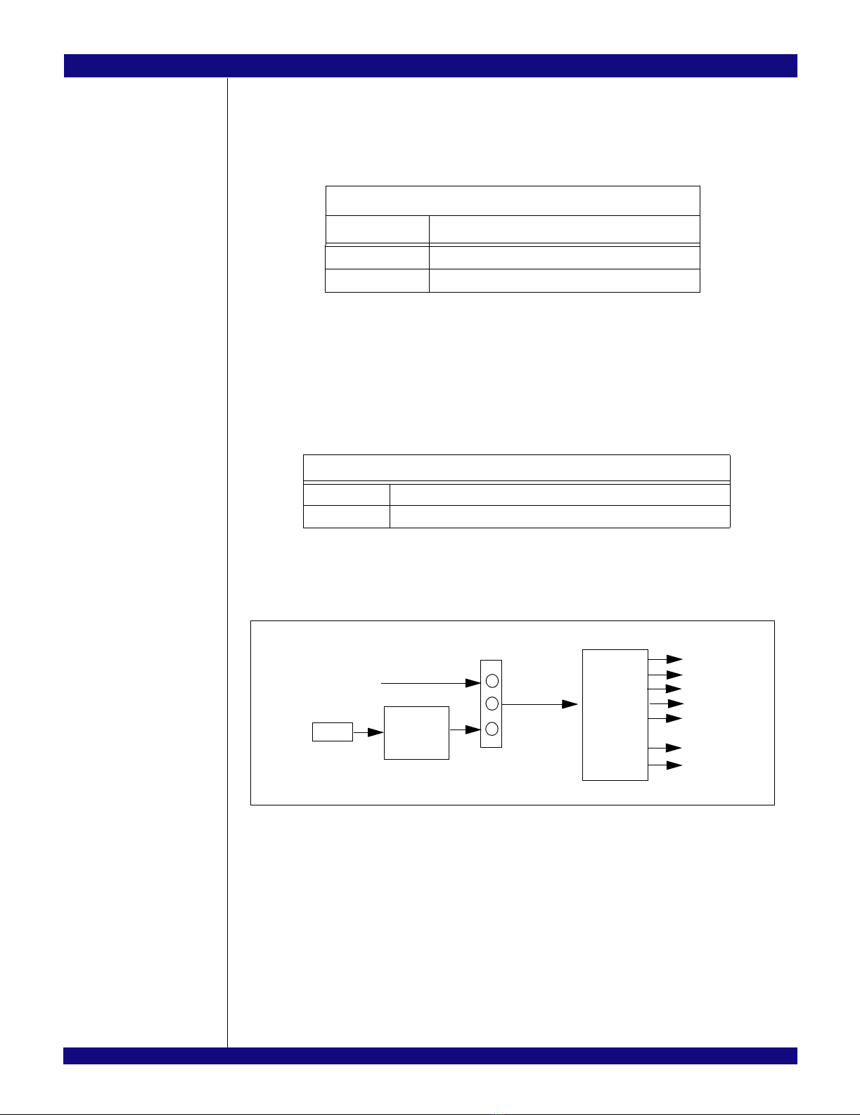
The 89HPES4T4 switch (also referred toas PES4T4 inthis manual) is a member of IDT’s PCI Express®
standard (PCIe®) based line of products. It is an 4-lane, 4-port switch. One upstream port is provided for
connecting to the rootcomplex (RC), and up to three downstreamports areavailable for connectingto PCIe
endpoints or to another switch. More information on this device can be found in the 89HPES4T4 User
Manual.
The 89EBPES4T4 Evaluation Board (also referred to as EB4T4 in this manual) provides an evaluation
platform for the PES4T4 switch. It is also a cost effective way to add a PCIe downstream port (x1) to an
existing system with a limited number of PCIe downstream ports. The EB4T4 eval board is designed to
function as an add-on card to beplugged into a x1 PCIe slot available on a motherboard hosting an appro-
priate root complex, microprocessor(s), and three downstream ports. The EB4T4 is a vehicle to test and
evaluate the functionality of the PES4T4 chip. Customers can use this board to get a headstart on software
development prior to the arrival of their own hardware. The EB4T4 is also used by IDT to reproduce
system-level hardware or software issues reported by customers. Figure 1.1 illustrates the functional block
diagram representing the main parts of the EB4T4 board.
Figure 1.1 Function Block Diagram of the EB4T4 Eval Board
JTAG
Header
Main
Reset
I/O Expander
PCA9555
PCIe x1 Upstream Edge
EEPROM
24LC512
SMBUS
HEADER
PES4T4
PCI Express
Switch
External Power
PCIe x1 Downstream Slot
x1
x1
25 MHz
SSC Clock
Buffer
Clock
Fanout
SMBus
Voltages on board
+12V, +3.3V, +1.5V, +1.0V
Connector
Power
Module
PTH08T240
x1
x1 x1
PCIe x1 Downstream Slot
PCIe x1 Downstream Slot

IDT Description of the EB4T4 Eval Board
EB4T4 Eval Board Manual 1 - 2 August 20, 2007
Notes Board Features
Hardware
PES4T4 PCIe 4 port switch
– Four ports (x1), 4 PCIe lanes
– PCIe Base Specification Revision 1.1 compliant
– Integrates four 2.5 Gbps embedded SerDes
– Up to 256 byte maximum Payload Size
– Automatic polarity inversion supported on all lanes
– Load configuration from an optional serial EEPROM via SMBUS
Upstream, Downstream Port
– One edge connector on the upstream port, to be plugged into a x1 slot on a host motherboard
– Threeslotconnectorsonthedownstreamports,forPCIeendpointadd-oncardstobeplugged in.
Numerous user selectable configurations set using onboard jumpers and DIP-switches
– Source of clock - host clock or onboard clock generator
– One clock rate (100 MHz) and spread spectrum setting
– Boot mode selection
Vaux Support
SMBUS Master Interface connected to the Serial EEPROMs through I/O expander
“Attention” button for each downstream port to initiate a hot swap event on each port
Four pin connector for optional external power supply
Push buttonfor Warm Reset
Several LEDs to display status, reset, power, “Attention”, etc.
One 10-pin JTAG connector (pitch 2.54 mm x 2.54 mm)
Software
There is no software or firmware executed on the board. However, useful software is provided along
with the Evaluation Board to facilitate configuration and evaluation of the PES4T4 within host systems
running popular operating systems.
Installation programs
– Operating Systems Supported: Windows2000, WindowsXP, Linux
GUI based application for Windows and Linux
– Allows users to view and modify registers in the PES4T4
– Binary file generator for programming the serial EEPROMs attached to the SMBUS.
Other
A metal bracket is required to firmly hold in place the three endpoints plugged into the EB4T4
board.
An external power supply may be required under some conditions.
SMBUS cable may be required for certain evaluation exercises.
SMA connectors are provided on the EB4T4 board for specific test points.
Revision History
August 20, 2007: Initial publication of board manual.

Notes
EB4T4 Eval Board Manual 2 - 1 August 20, 2007
®
Chapter 2
Installation of the EB4T4
Eval Board
EB4T4 Installation
This chapter discusses the steps required to configure and install the EB4T4 evaluation board. All avail-
able DIP switches and jumper configurations are explained in detail.
The primary installation steps are:
1. Configure jumper/switch options suitable for the evaluation or application requirements.
2. Connect PCI Express endpoint cards to the downstream port PCIe slots on the evaluation board.
3. Insert the evaluation board into the host system (motherboard with root complex chipset).
4. Apply power to the host system.
The EB4T4 board is shipped with all jumpers and switches configured to their default settings. In most
cases, the board does not require further modification or setup.
Hardware Description
The PES4T4 is an 4-lane, 4-port PCI Express® switch. It is a peripheral chip that performs PCI Express
based switching with a feature set optimized for high performance applications such as servers and
storage. It provides fan-out and switching functions between a PCI Express upstream port and three down-
stream ports or peer-to-peer switching between downstream ports.
The EB4T4 has three PCI Express downstream ports, accessible through three x4 open-ended connec-
tors.
Basic requirements for the board to run are:
– Host system with a PCI Express rootcomplex supporting x4 configuration througha PCIExpress
x1 slot.
– PCI Express Endpoint Cards capable of training x1 link.
Host System
The evaluation board cannot be operated as a standalone unit. A host system implementing a PCI
Express root complex supporting x1 configuration through a PCI Express x1 slot is required to take full
advantage of the PES4T4’s capabilities.
Reference Clocks
The PES4T4 uses one differential reference clock (100 MHz). The EB4T4 derives this clock from a
common source which is user-selectable. The common source can be either the host system’s reference
clock or the onboard clock generator. Selection is made by resistors described in Table 2.1.
Clock Configuration R32, R53, R51, R62
Installed Clock Source
R32, R53 Onboard Reference Clock – Use onboard clock generator
R51, R62 Upstream Reference Clock – Host system provides clock (Default)
Table 2.1 Clock Source Selection
IDT Installation of the EB4T4 Eval Board
EB4T4 Eval Board Manual 2 - 2 August 20, 2007
Notes The source for the onboard clock is the ICS9FG104 clock generator device (U8) connected to a 25MHz
oscillator (Y1). When using the onboard clock generator, the EB4T4 allows the selection of spread spec-
trum settings via DIP switches as described in Table 2.2 . Spread Spectrum technology reduces peak EMI
emissions by modulating the frequency to spread the peak energy over a wider bandwidth.
If the Clock Spread Spectrum is used to modulate data rate, then both ports must use same modulated
clock source. Therefore, if your system uses SSC, the on-board clock generator must be disabled and the
upstream reference clock should be used instead.
The output of the onboard clock generator is accessible through two SMA connectors located on the
Evaluation Board. See Table 2.3. This can be used to connect a scope for probing or capturing purposes
and cannot be used to drive the clock from an external source.
Figure 2.1 illustrates the clock distribution block diagram for the EB4T4 evaluation board.
Figure 2.1 Clock Distribution Block Diagram
Clock Spread Spectrum Switch - S3[2]
S3[2] Spread Spectrum
OFF Enable Spread Spectrum
ON Disable Spread Spectrum (Default)
Table 2.2 Spread Spectrum Clock Selection
Onboard Reference Clock Output (Differential) – J3, J1
J3 Positive Reference Clock
J1 Negative Reference Clock
Table 2.3 SMA Connectors - Onboard Reference Clock
PEREFCLK0
PEREFCLK1
Port2
Port3
Port4
Upstream PEREFCLK
25MHz
ICS9DB803D
SMA - J1
SMA - J3
ISC9FG104
Resistor Switch

IDT Installation of the EB4T4 Eval Board
EB4T4 Eval Board Manual 2 - 3 a
Notes Power Sources
Power for the EB4T4 is generated from the 12.0V PCI Express upstream slot power or optionally from
3.3Vaux. A 12.0V to 3.3V DC-DC converter will be used to provide power to four DC-DC converters to
generate VDDcore, VDDpe, VDDpea, and VTT voltages. The 3.3V from the 12.0V converter is used to
power VDDio. When in power down mode the DC-DC converters is powered directly from 3.3Vaux through
a MOSFET switch.
Figure 2.2 Power Distribution Block Diagram
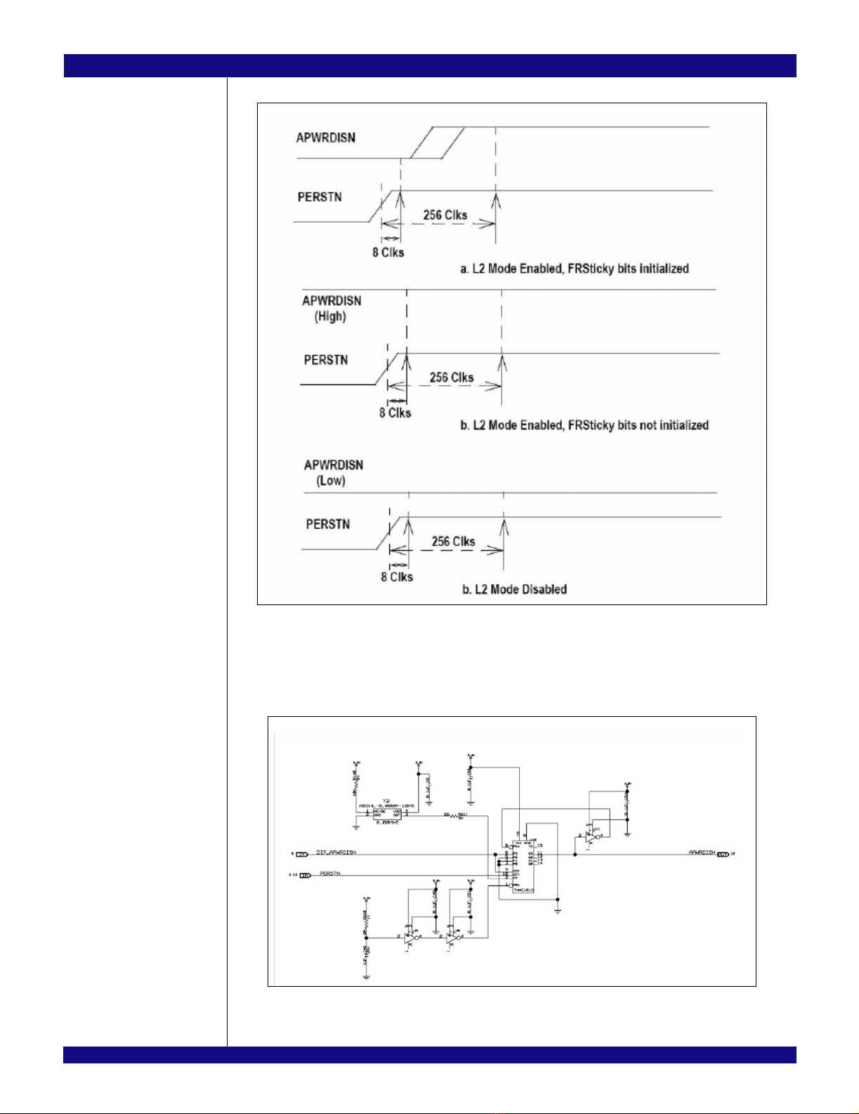
Vaux Support
Power supply support will be provided to EB4T4 from 12.0V upstream power to 3.3Vaux upstream
power when in sleep mode. The WAKE# signal direction, both an input and output will be supported by
jumper selection. The APWRDIS# signal for auxiliary power disable requires the following timing on power-
up:
IDT Installation of the EB4T4 Eval Board
EB4T4 Eval Board Manual 2 - 4 August 20, 2007
Notes
Figure 2.3 APWRDIS# Timing
On initial power up APWRDIS# must be held low initially for 8 clocks after PERST# is removed. Then it
must be sampled high 256 clocks after PERSTN# is removed to enable L2 mode. Subsequent PERST# will
not affect the APWRDIS# state. This timing will be provided by the following circuit.
Figure 2.4 APWRDIS# Timing Circuit

IDT Installation of the EB4T4 Eval Board
EB4T4 Eval Board Manual 2 - 5 a
Notes PCI Express Serial Data Transmit Termination Voltage Converter
A DC-DC converter (U6) provides a 1.5V PCI Express serial data transmit termination voltage (shown
as VTTPEor VPETVTT)to the PES4T4.
PCI Express Digital Power Voltage Converter
A separate DC-DC converter (U16) provides a 1.0V PCI Express digital power voltage (VDDPE) to the
PES4T4.
PCI Express Analog Power Voltage Converter
A separate DC-DC converter (U7) provides a 1.0V PCI Express analog power voltage (shown as
VDDAPE or VDDPEA)to the PES4T4.
Core Logic Voltage Converter
A separate DC-DC converter (U1) provides the 1.0V core voltage (VDDCORE) to the PES4T4.
3.3V I/O Power Module
A 12V to 3.3V power module (U5) provides the 3.3V I/O voltage (VDDIO) to the PES4T4.
Power-up Sequence
The power-up sequence must be as following:
1. VDDIO - 3.3V
2. VDDCORE, VDDAPE, VDDPE - 1.0V
3. VTTPE - 1.5V
When powering up, each voltage level must ramp up and stabilize prior to applying the next voltage in
the sequence to ensure internal latch-up issues are avoided. There are no maximum time limitations
between sequential valid power level requirements. To insure that the sequencing requirements are met, a
0.047µF is used at the SOFTSTART cap on the VTTPE’s voltage converter (U6 pin 36) in the EB4T4.
Required Jumpers
To deliver power to the PES4T4 switch, the following jumpers must be shunted: W4, W10, W23, W24,
and W25. These jumpers were implemented so that the power consumption of the PES4T4 can be
measured.
Reset
The PES4T4 supports two types of reset mechanisms as described in the PCI Express specification:
– Fundamental Reset: This is a system-generated reset that propagates along the PCI Express
tree through a single side-band signal PERST# which is connected to the Root Complex, the
PES4T4, and the endpoints.
– Hot Reset: This is an In-band Reset, communicated downstream via a link from one device to
another. Hot Reset maybeinitiatedbysoftware.Thisisfurtherdiscussedinthe89HPES8T4User
Manual. The EB4T4 evaluation board provides seamless support for Hot Reset.
Fundamental Reset
There are two types of Fundamental Resets which may occur on the EB4T4 evaluation board:
– Cold Reset: During initial power-on, the onboard voltage monitor (TLC7733D) will assert the PCI
Express Reset (PERSTN) input pin of the PES4T4.
– Warm Reset: This is triggered by hardware while the device is powered on. Warm Reset can be
initiated by two methods:
• Pressing a push-button switch (S1) located on EB4T4 board

IDT Installation of the EB4T4 Eval Board
EB4T4 Eval Board Manual 2 - 6 August 20, 2007
Notes • The host system board IO Controller Hub asserting PERST# signal, which propagates through
thePCIeupstreamedgeconnectoroftheEB4T4.Notethatonecanbypasstheonboardvoltage
monitor (TLC7733D) by moving the shunt from pin 1-2 to pin 2-3 (default) onW2.
Both events cause the onboard voltage monitor (TLC7733D) to assert the PCI Express Reset
(PERSTN) input of the PES4T4 while power is on.
Downstream Reset
The PES4T4 provides a a choice of either a software-controlled reset for each downstream port through
GPIO pins or a fundamental reset through PERST#. Selection is made by jumpers described in Table 2.4.
Boot Configuration Vector
A boot configuration vector consisting of the signals listed in Table 2.5 is sampled by the PES4T4 during
a fundamental reset (while PERSTN is active). The boot configuration vector defines the essential parame-
ters for switch operation and is set using DIP switches S3 and S5 as defined in Table 2.6.
Port # Jumper Selection
4 W9 [1-2] Software controlled reset through GPIO1
[2-3] Fundamental reset PERST# (default)
3 W6 [1-2] Software controlled reset through GPIO9
[2-3] Fundamental reset PERST# (default)
2 W7 [1-2] Software controlled reset through GPIO0
[2-3] Fundamental reset PERST# (default)
Table 2.4 Downstream Reset Selection
Signal Description
CCLKDS Common Clock Downstream. When the CCLKDS pin is asserted, it indicates that a com-
mon clock is being used between the downstream device and the downstream port.
Default: 0x1
CCLKUS Common Clock Upstream. When the CCLKUS pin is asserted, itindicatesthat a common
clock is being used between the upstream device and the upstream port. Default: 0x1
RSTHALT Reset Halt. When thissignal is asserted during a PCI Express fundamental reset, the
PES4T4 executes the reset procedure and remains in a reset state with the Master SMBus
active. This allows software to read and write registers internal to the device before normal
device operation begins. The device exits the reset state when the RSTHALT bit is cleared
in the P0_SWCTL register through the SMBus.
The value may be overridden by modifying the RSTHALT bit in the P0_SWCTL register.
Default: 0x0
SWMODE[2:0] Switch Mode. These configuration pins determine the PES4T4 switch operating mode.
Default: 0x1
0x0 - Normal switch mode
0x1 - Normal switch mode with Serial EEPROM-based initialization
0x2 through 0x8 - Reserved
APWRDIS# Auxiliary Power Disable. When this pin is active, it disables the device from using auxil-
iary power supply. Default: 0x0
Table 2.5 Boot Configuration Vector Signals

IDT Installation of the EB4T4 Eval Board
EB4T4 Eval Board Manual 2 - 7 a
Notes
SMBus Interfaces
The System Management Bus (SMBus) is a two-wire interface through which various system compo-
nent chips can communicate. It is based on the principles of operation of I2C. Implementation of the SMBus
signals in the PCI Express connector is optional and may not be present on the host system. The SMBus
interface consist of an SMBus clock pin and SMBus data pin.
SMBus Master Interface
Connected to the master SMBus interface are four 16-bit I/O Expanders (PCA9555) and a serial
EEPROM (24LC512). Four I/O Expanders are used as the interface for the onboard hot-plug controllers
(MIC2591B). The Master SMBus interface provides connection to the external serial EEPROMs used for
initialization and the I/O expander used for hot-plug signals.
The bus address for the selected EEPROM device is 0b1010011 by default.
The PES4T4 provides a JTAG connector J4 for access tothe PES4T4 JTAGinterface. The connector is
a 2.54 x 2.54 mm pitch male 10-pin connector. Refer to Table 2.9 for the JTAG Connector J2 pin out.
Attention Buttons
The PES4T4 features four attention buttons, shown in Table 2.10. Each button corresponds to a partic-
ular port and is used to initiate hot-swapping events.
Signal Description Default
S3[4] CCLKDS OFF
S3[5] CCLKUS OFF
S5[6] RSTHALT ON
S5[1] SWMODE[0] ON
S5[2] SWMODE[1] ON
S5[3] SWMODE[2] ON
S5[5] APWRDIS# ON
Table 2.6 Boot Configuration Vector Switches S3 and S5 (ON=0, OFF=1)
JTAG Connector J2
Pin Signal Direction Pin Signal Direction
1 /TRST - Test reset Input 2 GND —
3 TDI - Test data Input 4 GND —
5 TDO - Test data Output 6 GND —
7 TMS - Test mode select Input 8 GND —
9 TCK - Test clock Input 10 GND —
Table 2.7 JTAG Connector Pin Out

IDT Installation of the EB4T4 Eval Board
EB4T4 Eval Board Manual 2 - 8 August 20, 2007
Notes
Miscellaneous Jumpers, Headers
Button Description
SW3 Port 4 Attention Button
SW2 Port 3 Attention Button
SW1 Port 2 Attention Button
Table 2.8 Attention Buttons
Miscellaneous Jumpers, Headers
Ref.
Designator Type Default Description
S2[1] Switch OFF Port2: Manually-operated Retention Latch
S2[2] Switch OFF Port3: Manually-operated Retention Latch
S2[3] Switch OFF Port4: Manually-operated Retention Latch
S6[3] Switch OFF Bypass hot-plug controller - Enables direct power (+12V and
+3.3V) to Ports 4 (Default)
S6[2] Switch OFF Bypass hot-plug controller - Enables direct power (+12V and
+3.3V) to Ports 3 (Default)
S6[1] Switch OFF Bypass hot-plug controller - Enables direct power (+12V and
+3.3V) to Ports 2 (Default)
W32 Header 2-3 Shunted 1-2: Port 2, +3.3V source base on hot-plug controller
2-3: Port 2, +3.3V source from upstream port power
W31 Header 2-3 Shunted 1-2: Port 2, +12V source base on hot-plug controller
2-3: Port 2, +12V source from upstream port power
W30 Header 2-3 Shunted 1-2: Port 2, +3.3Vaux source base on hot-plug controller
2-3: Port 2, +3.3Vaux source from upstream port power
W35 Header 2-3 Shunted 1-2: Port 3, +3.3V source base on hot-plug controller
2-3: Port 3, +3.3V source from upstream port power
W34 Header 2-3 Shunted 1-2: Port 3, +12V source base on hot-plug controller
2-3: Port 3, +12V source from upstream port power
W33 Header 2-3 Shunted 1-2: Port 3, +3.3Vaux source base on hot-plug controller
2-3: Port 3, +3.3Vaux source from upstream port power
W38 Header 2-3 Shunted 1-2: Port4, +3.3V source base on hot-plug controller
2-3: Port 4, +3.3V source from upstream port power
W37 Header 2-3 Shunted 1-2: Port 4, +12V source base on hot-plug controller
2-3: Port 4, +12V source from upstream port power
W36 Header 2-3 Shunted 1-2: Port 4, +3.3Vaux source base on hot-plug controller
2-3: Port 4, +3.3Vaux source from upstream port power
W15 Header Open 1-2: Select WAKEN# as an input
2-3: Select WAKE# as in output
Table 2.9 Miscellaneous Jumpers, Headers (Part 1 of 2)

IDT Installation of the EB4T4 Eval Board
EB4T4 Eval Board Manual 2 - 9 a
Notes
LEDs
There are several LED indicators on the EB4T4 which convey status feedback. A description of each is
provided in Table 2.13.
W17 Header Shunted Power Good Enable Force On jumper for ICS90DB803 clock
output enable (OE4#)
W18 Header Shunted Power Good Enable Force On jumper for ICS90DB803 clock
output enable (OE3#)
W19 Header Shunted Power Good Enable Force On jumper for ICS90DB803 clock
output enable (OE2#)
W5 Header Open Special usage when there is no +12V power supply from the
upstream port. Require external power to connector J4.
Location Color Definition
DS87 Green Port 2: Power-is-good indicator
DS86 Green Port 3: Power-is-good indicator
DS85 Green Port 4: Power-is-good indicator
DS83 Amber Port2: Attention Input indicator
DS82 Amber Port3: Attention Input indicator
DS81 Amber Port4: Attention Input indicator
DS79 Green Port2: Presence Detect indicator
DS78 Green Port3: Presence Detect indicator
DS77 Green Port4: Presence Detect indicator
DS64 Amber Port2: Attention Output indicator
DS63 Amber Port3: Attention Output indicator
DS62 Amber Port4: Attention Output indicator
DS57 Green Port 2: Power indicator
DS56 Green Port 3: Power indicator
DS55 Green Port 4: Power indicator
DS91 Red Port 2: MRL indicator
DS90 Red Port 3: MRL indicator
DS89 Red Port 4: MRL indicator
DS95 Red Port 2: Power Fault indicator
DS94 Red Port 3: Power Fault indicator
DS93 Red Port 4: Power Fault indicator
Table 2.10 LED Indicators (Part 1 of 2)
Miscellaneous Jumpers, Headers
Ref.
Designator Type Default Description
Table 2.9 Miscellaneous Jumpers, Headers (Part 2 of 2)

IDT Installation of the EB4T4 Eval Board
EB4T4 Eval Board Manual 2 - 10 August 20, 2007
Notes
PCI Express Connectors
DS99 Green Port 2: Link Up indicator
DS98 Green Port 3: Link Up indicator
DS97 Green Port 4: Link Up indicator
DS100 Green Port 0: Link Up indicator
DS105 Amber Port0: Link Activity indicator
DS104 Amber Port2: Link Activity indicator
DS103 Amber Port3: Link Activity indicator
DS102 Amber Port4: Link Activity indicator
Pin Side A Side B
1 +12V 12V power PRSNT1# Hot-Plug presence detect
2 +12V 12V power +12V 12V power
3 RSVD Reserved +12V 12V power
4 GND Ground GND Ground
5 SMCLK SMBus clock JTAG2 TCK (Test Clock) JTAG i/f clki/p
6 SMDAT SMBus Data JTAG TDI (Test Data Input)
7 GND Ground JTAG TDO (Test Data Output)
8 +3.3V 3.3V power JTAG TMS (Test Mode Select)
9 JTAG1 TRST#(Test/Reset)resets
JTAG i/f +3.3V 3.3V power
10 3.3Vaux 3.3V auxiliary power +3.3V 3.3V power
11 WAKE# Signal for Link reactivation PERST# Fundamental Reset
Mechanical Key
12 RSVD Reserved GND Ground
13 GND Ground REFCLK+ REFCLK Reference clock
14 PETp0 Transmitter differential REFCLK- (differential pair)
15 PETn0 pair, Lane 0 GND Ground
16 GND Ground PERp0 Receiver differential
17 PRSNT2# Hot-Plug presence detect PERn0 pair, Lane 0
18 GND Ground GND Ground
19 PETp1 Transmitter differential RSVD Reserved
20 PETn1 pair, Lane 1 GND Ground
21 GND Ground PERp1 Receiver differential
Table 2.11 PCI Express x4 Connector Pinout (Part 1 of 2)
Location Color Definition
Table 2.10 LED Indicators (Part 2 of 2)
Table of contents
Other IDT Motherboard manuals


Popular Motherboard manuals by other brands


Texas Instruments
Texas Instruments bq24261M user guide

Supero
Supero SUPER S2DG2 User's and bios manual

ECS Electronics
ECS Electronics SI54P AIO user manual

Texas Instruments
Texas Instruments INA4290 user guide

Asus
Asus P5WDG2 WS Professional user manual

NXP Semiconductors
NXP Semiconductors OM13260 installation guide


