IDT 8T49N240 User manual

1©2017 Integrated Device Technology, Inc. June 6, 2017
Introduction
The 8T49N240, 8T49N241 and 8T49N242 evaluation boards are designed to help the customer evaluate the 8T49N240i, 8T49N241, and
8T49N242 devices, respectively. For the sake of simplicity this User Guide refers to the 8T49N242i evaluation board though all
statements also apply to the 8T49N240 and 8T49N241 evaluation board. When the board is connected to a PC running IDT Timing
Commander™ Software through USB, the device can be configured and programmed to generate frequencies with best-in-class
performances.
Requirements
▪PC Requirements:
— IDT Timing Commander Software Installed
— USB 2.0 or 3.0 interface
— Windows XP SP3 or later
— Processor: Minimum 1GHz
— Memory: Minimum 512MB, recommended 1GB
— Available Disk Space: Min 600MB (1.5GB, 64-bit), recommended 1GB (2GB 64-bit)
— Network access during installation if the .NET framework is not currently installed on the system
▪Power Supply with 3.3V and 1000mA rating
▪Four banana plug cables to connect the power supply to the board
Quick Start: Powering Up the Board
1. Set 3.3V supply current limit to 500mA.
2. Remove all output terminations.
3. Set Dip Switch selectors to the middle position.
4. Connect a cable from a PC to the USB port.
5. Connect VEE to the GND jack.
6. Connect 3.3V to Vcc_J, Vcca_J, and Vcco_J jacks.
7. Power on the Power Supply.
8. Press the Reset Button.
Once correct operation is verified, set the power supply limit for the number of outputs to be active.
The USB port must be powered by the PC in order to have the correct I2C bus voltage levels.
Default Power-Up Condition
The 8T49N241 and 8T49n242 boards ship with a 38.88MHz surface-mount crystal populated on the top of the board. The 8T49N240
board ships with a 49.152MHz crystal. If a different crystal frequency is needed, this part must be removed (for more information, see
Crystal Interface).
All outputs should be off and the current should measure ~236mA with 3.3V on Vcc_J, Vcca_J, and Vcco_J.
When evaluating performance with the default hardware configuration, it is recommended that all active outputs be terminated 50ohms to
VEE by either terminator plugs or an instrument.
8T49N24x Evaluation Board User Guide
2©2017 Integrated Device Technology, Inc. June 6, 2017
8T49N24x Evaluation Board User Guide
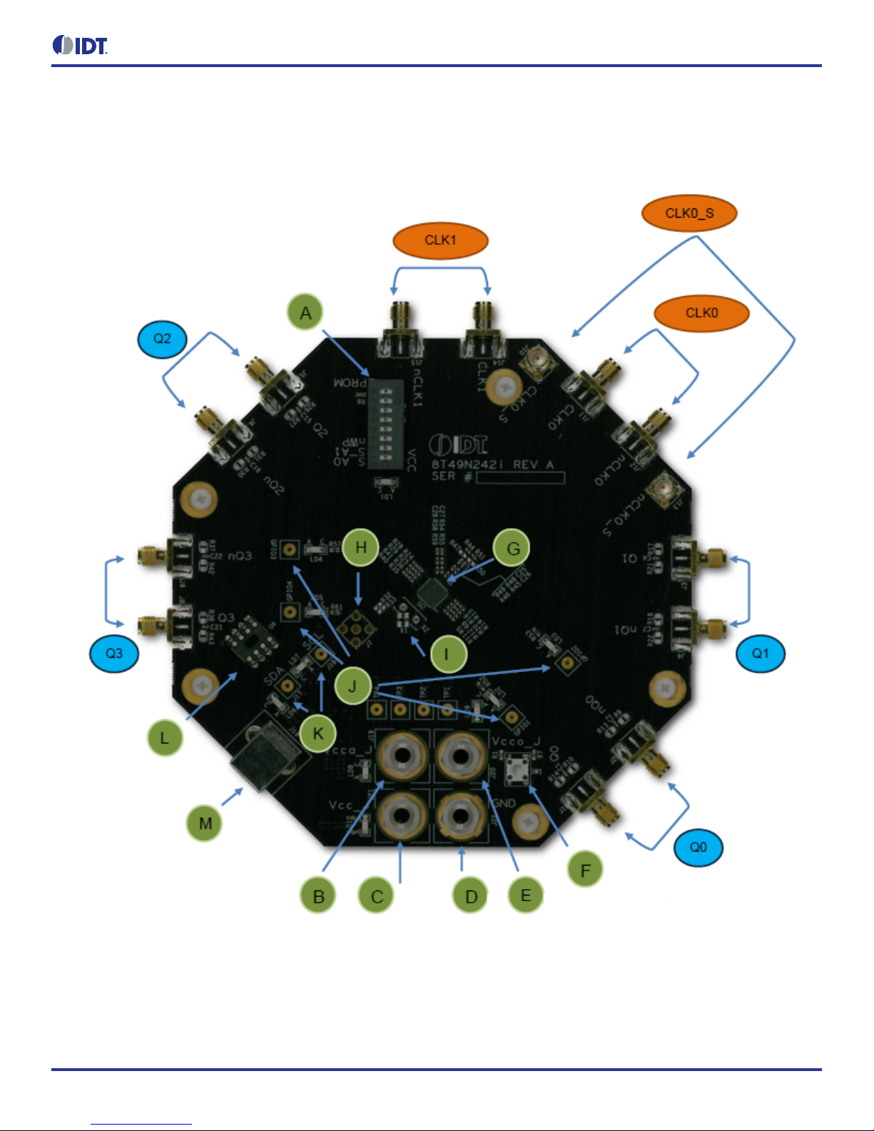
Board Overview
Use the following diagram to identify and locate: power supply jacks, USB connector, input and output SMA connectors, reset button,
EEPROM, etc.
Figure 1. Evaluation Board Overview

3©2017 Integrated Device Technology, Inc. June 6, 2017
8T49N24x Evaluation Board User Guide
Legend–Evaluation Board
Inputs
Outputs
Other
CLK0_S Clock 0 sense lines.
CLK0 Clock 0 input lines. Can be configured for differential or single-ended input.
CLK1 Clock 1 input lines. Can be configured for differential or single-ended input.
Q0 Output Q0. Can be a differential pair or two individual single-ended outputs.
Q1 Output Q1. Can be a differential pair or two individual single-ended outputs
Q2 Output Q2. Can be a differential pair or two individual single-ended outputs.
Q3 Output Q3. Can be a differential pair or two individual single-ended outputs.
A Dip Switch for DC control signals (EEPROM_WP, S_A0/1, nWP)
B Vcca_J
CVcc_J
DGND
E Vcco_J
F RESET
G IDT8T49N24x- the device to be evaluated
H OSCI crystal overdrive connector (not installed by default)
I Crystal connectors (HC49/US through-hole socket and 3.2x2.5 SMD footprint)
J GPIO test points
K I2C test points
L EEPROM socket (AT24C04C)
M USB connector

4©2017 Integrated Device Technology, Inc. June 6, 2017
8T49N24x Evaluation Board User Guide
Software GUI Overview
The 8T49N24x devices are programmed using IDT's Timing Commander software, which provides an interactive and intuitive Graphical
User Interface to program and adjust the many settings that are available for the devices. Timing Commander is the generic platform
upon which many devices' GUIs run on. Each GUI has a file called a “personality” that is loaded by Timing Commander so that it can
interface with the supported devices. Timing Commander installation and personality files, as well as tutorials and support are available at
http://www.idt.com/products/clocks-timing/timing-commander-software-download-resource-guide. The GUI for the 8T49N24x devices is
shown below.
Figure 2. Timing Commander 8T49N24x GUI

5©2017 Integrated Device Technology, Inc. June 6, 2017
8T49N24x Evaluation Board User Guide
Schematics
The following figures are schematics that are applicable to specific sections of this User Guide. The complete schematics are available in
a separate document.
Figure 3. Inputs Schematic
6©2017 Integrated Device Technology, Inc. June 6, 2017
8T49N24x Evaluation Board User Guide
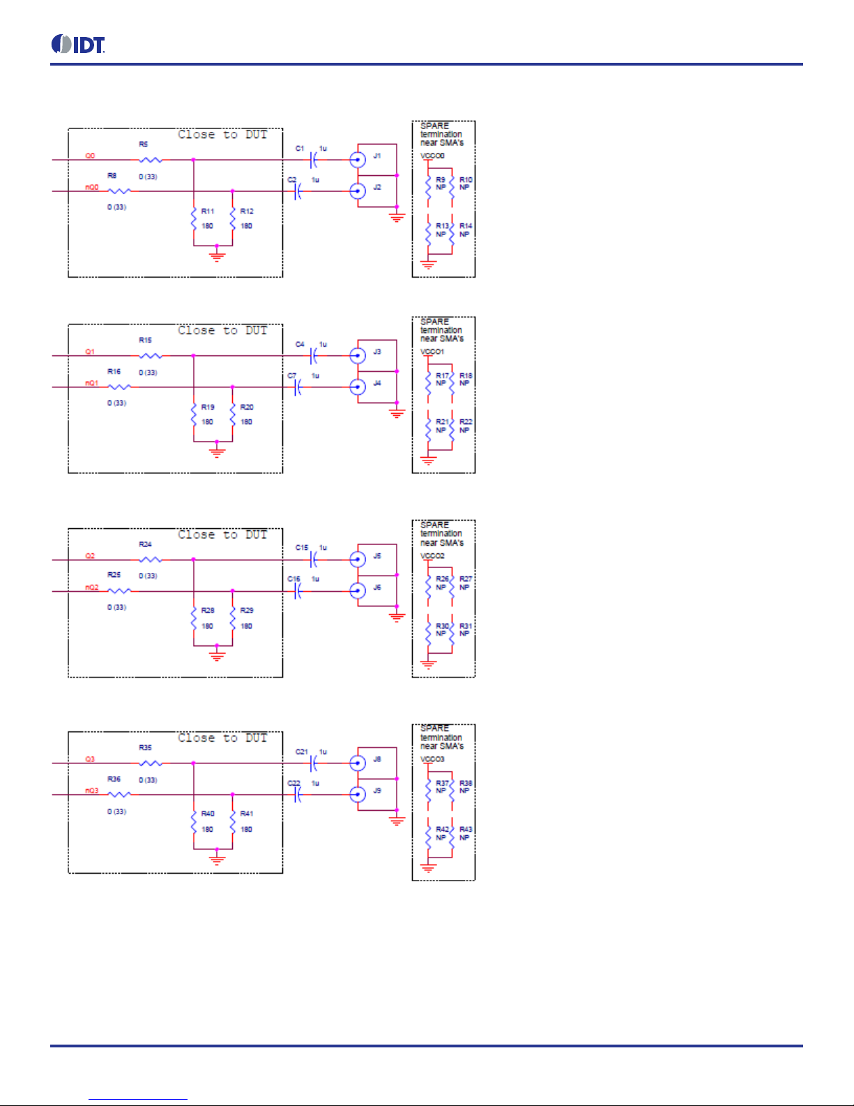
Figure 4. Output Termination Schematic
7©2017 Integrated Device Technology, Inc. June 6, 2017
8T49N24x Evaluation Board User Guide
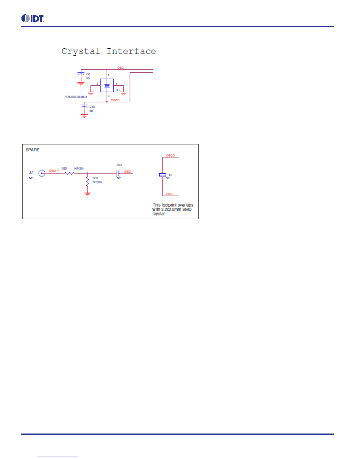
Figure 5. Crystal Interface Schematic

8©2017 Integrated Device Technology, Inc. June 6, 2017
8T49N24x Evaluation Board User Guide
Figure 6. EEPROM/I2C Schematic

9©2017 Integrated Device Technology, Inc. June 6, 2017
8T49N24x Evaluation Board User Guide
Figure 7. DC Control Schematic
Figure 8. GPIOs Schematic

10©2017 Integrated Device Technology, Inc. June 6, 2017
8T49N24x Evaluation Board User Guide
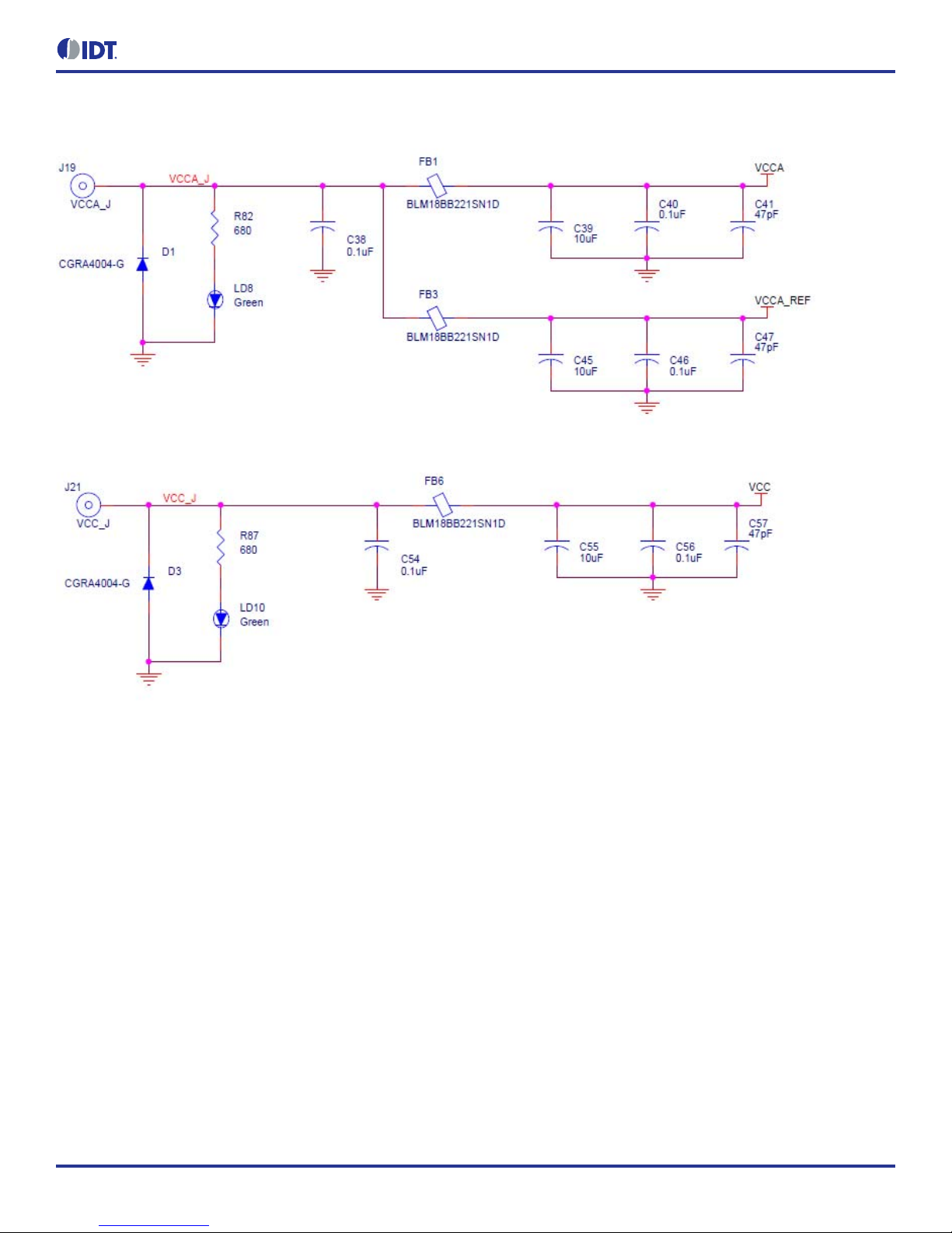
Figure 9. VCCO Power Filtering Schematic
11©2017 Integrated Device Technology, Inc. June 6, 2017
8T49N24x Evaluation Board User Guide
Figure 10. VCC Power Filtering Schematic
12©2017 Integrated Device Technology, Inc. June 6, 2017
8T49N24x Evaluation Board User Guide
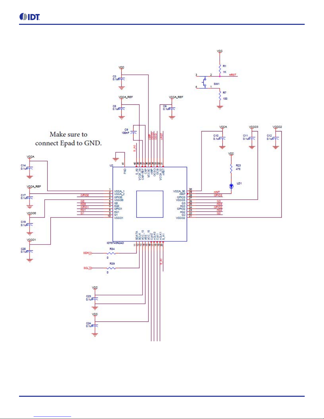
Figure 11. 8T49N241 and 8T49N242 DUT Schematic

13©2017 Integrated Device Technology, Inc. June 6, 2017
8T49N24x Evaluation Board User Guide
Figure 12. 8T49N240 DUT Schematic

14©2017 Integrated Device Technology, Inc. June 6, 2017
8T49N24x Evaluation Board User Guide
Board Power Supply
Core Voltages
The core voltage includes a digital supply voltage VCC and an analog supply voltage VCCA. The digital supply voltage is powered by an
external bench power supply connected to J19 (VCCA_J). The analog supply voltage is powered by an external bench power supply
connected to J21 (VCC_J) (see Figure 9).
Output Voltages
VDDO_J (J1) supplies the global voltage for the outputs and can be biased by the external power supply at 1.8V (using LVCMOS for all
outputs), 2.5V, or 3.3V.
Mixed Voltage Operation
This board provides the option to operate the outputs with a mixed combination of output voltages. Refer to Figure 8 for a complete view
of the VCCO schematic. Each VCCOx has a 0resistor that connects it to the global VCCO_J power rail. This resistor can be removed
and the voltage can be provided using the test point. For example, the schematic below can be configured so that Q0 (VCCO0) operates
at 2.5V and Q1 (VCCO1) operates at LVCMOS 1.8V as follows:
1. Connect 2.5V to J20 (VCCO_J).
2. Remove R85. This isolates VCCO1 from global VCCO_J.
3. Solder a wire onto test point TP2 and bias with a 1.8V supply.
Figure 13. Mixed Output Voltage Operation

15©2017 Integrated Device Technology, Inc. June 6, 2017
8T49N24x Evaluation Board User Guide
Input Configuration
The inputs are configured with an AC-coupling termination scheme. This scheme allows flexibility for either differential or single-ended
inputs. The default configuration is as follows:
Differential Input
Connect the input signal to CLKx and nCLKx. For CLK0, the CLK0_S and nCLK0_s sense lines are available for observation of the
signal. They can be connected with 50ohm impedance cables to an oscilloscope with 50ohm termination, otherwise, they should be
terminated with 50ohm plugs in order prevent reflections. The CLK1 input is 50ohm terminated to ground.
Single-ended Input
Connect the input signal to CLKx and float nCLKx. For CLK0, connect CLK0_S with a 50ohm impedance cable to an oscilloscope with
50ohm termination or terminate with a 50ohm plug.
Input Signals Below 1MHz
For slow-frequency signals below 1MHz, we recommend that the AC-coupling capacitors for the corresponding input be replaced with
zero-ohm resistors and that the signal input DC-offset be set so that it meets the device's Vcmr requirements. Refer to Figure 3 to locate
the components listed below.
Table 1. Default Input Configuration
Input Default Termination Sense Lines
CLK0 Unterminated, AC-coupled into the device and terminated
via sense line connector to equipment or termination
connector.
Use SMAs J10/J13 for observation of the input signal
and termination of the input signal
CLK1 Terminated, AC-coupled into the device Not available
Table 2. Input Termination Schemes
Signal
Frequency AC-coupling capacitors:
CLK0 (C25, C26); CLK1 (C27,C28) Input Signal DC Offset
>1MHz 1uF Don’t care
<1MHz 0 ΩMust meet datasheet Vcmr specs

16©2017 Integrated Device Technology, Inc. June 6, 2017
8T49N24x Evaluation Board User Guide
Output Configuration
The outputs are AC-coupled, allowing for maximum flexibility for observation of the output whether configured for LVPECL, LVDS,
LVCMOS, or HCSL levels. The default termination scheme can be used to measure any of the three output level-types but is not optimal.
The optimal termination circuits are tabulated below. Refer to Figure 4 to locate the components listed below.
Table 3. Termination Outputs for Q0
Signal Type Source resistors:
R5, R8 180ohm pull-down:
R11, R12 Series capacitors:
C1,C2 Spare Resistors:
R9, R10, R13, R14
LVPECL (Default) 0ohm Installed 1uF Not Installed
LVCMOS 33ohm Not Installed 1uF Not Installed
LVDS 0ohm Not Installed 1uF Not Installed
HCSL 33ohm Not Installed 1uF Not Installed
Table 4. Termination Outputs for Q1
Signal Type Source resistors:
R15, R16 180ohm pull-down:
R19, R20 Series capacitors:
C4,C7 Spare Resistors:
R17, R18, R21, R22
LVPECL (Default) 0ohm Installed 1uF Not Installed
LVCMOS 33ohm Not Installed 1uF Not Installed
LVDS 0ohm Not Installed 1uF Not Installed
HCSL 33ohm Not Installed 1uF Not Installed
Table 5. Termination Outputs for Q2
Signal Type Source resistors:
R24, R25 180ohm pull-down:
R28, R29 Series capacitors:
C15,C16 Spare Resistors:
R26, R27, R30, R31
LVPECL (Default) 0ohm Installed 1uF Not Installed
LVCMOS 33ohm Not Installed 1uF Not Installed
LVDS 0ohm Not Installed 1uF Not Installed
HCSL 33ohm Not Installed 1uF Not Installed
Table 6. Termination Outputs for Q3
Signal Type Source resistors:
R35, R36 180ohm pull-down:
R40, R41 Series capacitors:
C21,C22 Resistor Network:
R37,R38, R42, R43
LVPECL (Default) 0ohm Installed 1uF Not Installed
LVCMOS 33ohm Not Installed 1uF Not Installed
LVDS 0ohm Not Installed 1uF Not Installed
HCSL 33ohm Not Installed 1uF Not Installed

17©2017 Integrated Device Technology, Inc. June 6, 2017
8T49N24x Evaluation Board User Guide
Output Signals Below 1MHz
For output signals below 1MHz we recommend that the 1uF AC-coupling capacitors be replaced with 0ohm resistors and that the correct
terminations be provided at the receiver.
EEPROM Boot
The evaluation board ships with an IDT8T49N24x-998 device, which will attempt to boot from the EEPROM at power-up. If an EEPROM
is not present, the device registers will need to be set by Timing Commander. The EEPROM must have at least 85 bytes, have an I2C
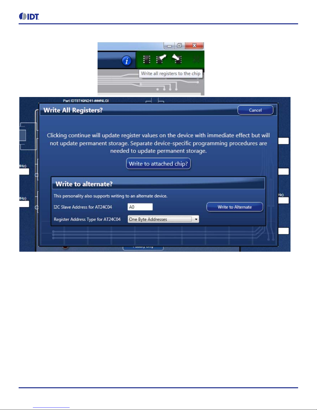
address of 0xA0, use 1-byte addressing, and conform to the 8-DIP package shown in Figure 1 (symbol “L”) and Figure 6. An AT24C04 is
typically used. The EEPROM is programmed through Timing Commander. Once connected to the chip using the “Connect to the chip”
button in the top-right corner of the window, a button for “Write All” will appear that is used to write all registers to either the IDT8T49N24x
device or the EEPROM.
Table 7. Spare Resistor Termination for LVPECL for Q0
Signal Type Source resistors:
R5, R8 180ohm pull-down:
R11, R12 Series capacitors:
C1,C2 Spare Resistors:
R9, R10, R13, R14
LVPECL (Default) 0ohm Not Installed 0ohm R9=R10=125ohm
R13=R14=84ohm
HCSL 33ohm Not Installed 0ohm R9=R10=Not Installed
R13=R14=50ohm
18©2017 Integrated Device Technology, Inc. June 6, 2017
8T49N24x Evaluation Board User Guide
Figure 14. EEPROM Programming
To write to the EEPROM, make sure the I2C slave address is set to 0xA0 and the address type is set to “One Byte Addresses”, then click
“Write to Alternate”. A confirmation message box will appear when the write is completed.
DC Controls
The DIP switch has three settings: 0V, Float, and VCC. This board ships with all switches in the Float (middle) position. Refer to Figure 1,
label “A” for the location of the DIP Switch. The functions for the switches are:
▪S1: 8T49N24x I2C slave address bit 0
▪S2: 8T49N24x I2C slave address bit 1
▪S3: 8T49N24x nWP, 0=Registers write protected, 1=Normal operation

19©2017 Integrated Device Technology, Inc. June 6, 2017
8T49N24x Evaluation Board User Guide
Crystal Interface
The board supports three types of crystals that can be used for the local reference oscillator of the device. If overdriving the crystal
oscillator with an external signal, an optional extra connector must be attached to allow this. The board ships with a 38.88MHz
surface-mount crystal populated in X1. If a different crystal is desired, or if overdriving the crystal oscillator externally, this part must be
removed. See Figure 1, label “I”. Crystal load capacitors support a 12pF crystal. If a crystal with a different load capacitance is used, C8
and C13 may need to be modified. These capacitors are on the bottom side of the board, next to the through-hole crystal socket (see
Figure 15).
Figure 15. Crystal Load Capacitors
1. Through-hole crystal. With this option, the device can be evaluated with different crystals without the need to solder each time the
crystal is replaced. Insert the crystal into the socket labeled X2 on the board (see Figure 1, label “I”).
2. Surface-mount crystal. With this option, a 3.2x2.5 SMD crystal may be soldered onto the footprint labeled X1 on the board (see
Figure 1, label “I”). The board ships with a 38.88MHz crystal installed here.
3. External Crystal Overdrive. With this option, the device can be evaluated using an external source, such as a frequency generator, XO,
or other device. The following modifications are needed for this option (see Figure 1 and Figure 4 for identification and location of the
components):
a. Populate SMA J7 (see Figure 1, label “H”).
b. Solder a 1uF capacitor onto C18. Note: The input must be AC-coupled.
c. R33 may be populated with a 50ohm resistor for input sources requiring such termination.
d. Populate R32 with either a 0ohm or 33ohm (LVCMOS) resistor.

20©2017 Integrated Device Technology, Inc. June 6, 2017
8T49N24x Evaluation Board User Guide
Application Notes and Resources
Design guidelines and resources may be found online for the 8T49N24x devices, at the following addresses:
8T49N240
http://www.idt.com/8T49N240
8T49N241
http://www.idt.com/8T49N241
8T49N242
http://www.idt.com/8T49N242
The site contains a wealth of information, including:
▪Device datasheets and errata
▪Package and dash-code options and ordering guide
▪Evaluation board resources, including guides and schematics
▪Cadence schematic symbols and footprints
▪IBIS simulation models
▪Application notes, including power-up configuration, frequency programming, EEPROM programming, output termination guidelines,
and more
▪Timing Commander installation and 8T49N24x personality files to allow programming of settings and creation of settings files used to
create new dash-codes from a PC
▪Example settings files and phase noise plots
▪Tutorial videos for Timing Commander and the 8T49N24x evaluation boards
For more questions or support, please submit a technical support request.
This manual suits for next models
4
Table of contents
Other IDT Motherboard manuals

IDT
IDT 9FGV1005 Operating instructions

IDT
IDT ZSSC4151 User guide

IDT
IDT VersaClock 6E 5P49V6965 User manual

IDT
IDT 8A34xxx 48QFN series User manual

IDT
IDT Tsi382 LQFP User manual

IDT
IDT ZWIR4532 User manual

IDT
IDT EB8T5A Eval Board User manual

IDT
IDT 82V3911 User manual

IDT
IDT ZSSC4151 User manual

IDT
IDT ZNRG2061 User manual


 user guide")


