IDT ADC1410S Series User manual

Quick start ADC1410S,
ADC1210S, ADC1010S series
Demonstration board for ADC1410S, ADC1210S, ADC1010S
series
Rev. 06 —2 July 2012
Quick start
Document information
Info
Content
Keywords
PCB2001-2, demonstration board, ADC, converter, input buffer
Abstract
This document describes how to use the demonstration board for the
analog-to-digital converter ADC1410S, ADC1210S and ADC1010S
series.
Overview

Integrated Device Technology
Quick start ADC1410S, ADC1210S, ADC1010S series
Quick start
© IDT 2012. All rights reserved.
Quick start
Rev. 06 —2 July 2012
2 of 27
Revision history
Rev
Date
Description
1
20081001
Initial version.
2
20090518
Update to PCB2001-2.
3
20090610
Add SPI software description.
4
20100519
Add HSDC extension module acquisition system description.
5
20110120
Update with latest software tool.
6
20120702
Rebranded.

Integrated Device Technology
Quick start
Quick start ADC1410S, ADC1210S, ADC1010S series
Quick start
Rev. 06 —2 July 2012
3 of 27
1. Overview of the ADC1410S, ADC1210S, ADC1010S demo board
1.1 ADC1410S series
Figure below presents the connections to measure ADC1410S.
Fig 1. ADC1410S series typical configuration set-up
PRESENTED CONFIGURATION
. 2Vpp input full scale
. Single Sine wave clock signal
. Input common mode from IC
. Binary ADC output
. SPI Mode
INPUT SIGNAL
. 2Vpp sinewave
. AC
SYNTHESIZED
SIGNAL
GENERATOR
FILTER
. High-order
. Band pass
POWER SUPPLY
. I = 185 mA
. N.C.
. 3V
.GND
POWER SUPPLY
. I = 20 mA
.GND
.1.8V
LOGIC ANALYZER
Output data
. DAV for synchronization
. D0 (LSB) to D13 (MSB)
CLOCK SIGNAL
. sinewave
. AC
SYNTHESIZED
SIGNAL
GENERATOR
SPI MODULE
USB OR PARALLEL

Integrated Device Technology
Quick start
Quick start ADC1410S, ADC1210S, ADC1010S series
Quick start
Rev. 06 —2 July 2012
4 of 27
1.2 ADC1210S series
Figure below presents the connections to measure ADC1210S.
Fig 2. ADC1210S series typical configuration set-up
PRESENTED CONFIGURATION
. 2Vpp input full scale
. Single Sine wave clock signal
. Input common mode from IC
. Binary ADC output
. SPI Mode
INPUT SIGNAL
. 2Vpp sinewave
. AC
SYNTHESIZED
SIGNAL
GENERATOR
FILTER
. High-order
. Band pass
POWER SUPPLY
. I = 185 mA
. N.C.
. 3V
.GND
POWER SUPPLY
. I = 20 mA
.GND
.1.8V
LOGIC ANALYZER
Output data
. DAV for synchronization
. D0 (LSB) to D11 (MSB)
CLOCK SIGNAL
. sinewave
. AC
SYNTHESIZED
SIGNAL
GENERATOR
SPI MODULE
USB OR PARALLEL

Integrated Device Technology
Quick start
Quick start ADC1410S, ADC1210S, ADC1010S series
Quick start
Rev. 06 —2 July 2012
5 of 27
1.3 ADC1010S series
Figure below presents the connections to measure ADC1010S.
Fig 3. ADC1010S series typical configuration set-up
PRESENTED CONFIGURATION
. 2Vpp input full scale
. Single Sine wave clock signal
. Input common mode from IC
. Binary ADC output
. SPI Mode
INPUT SIGNAL
. 2Vpp sinewave
. AC
SYNTHESIZED
SIGNAL
GENERATOR
FILTER
. High-order
. Band pass
POWER SUPPLY
. I = 185 mA
. N.C.
. 3V
.GND
POWER SUPPLY
. I = 20 mA
.GND
.1.8V
LOGIC ANALYZER
Output data
. DAV for synchronization
. D0 (LSB) to D9 (MSB)
CLOCK SIGNAL
. sinewave
. AC
SYNTHESIZED
SIGNAL
GENERATOR
SPI MODULE
USB OR PARALLEL

Integrated Device Technology
Quick start ADC1410S, ADC1210S, ADC1010S series
Quick start
© IDT 2012. All rights reserved.
Quick start
Rev. 06 —2 July 2012
6 of 27
1.4 Power supply
The board is powered with a 3 VDC and 1.8/3 VDC power supplies. A power supply regulator is
used to supply all the circuitry on the board.
Table 1. General power supply
Name
Function
View
J10
+3V green connector –Power supply 3 VDC / 250 mA.
J9
+1.8V green connector –Power supply 1.8 VDC / 100 mA
TP1
AGND test point –Digital ground
TP2
DGND test point –Analog ground
1.5 Input signals (IN, CLK)
The input clock signal can be either a sine-wave or a LVCMOS signal.
To ensure a good evaluation of the device, the input signal and the input clock must be
synchronized together.
Moreover, the input frequency (Fi, MHz) and the clock frequency (Fclk, Msps) should follow
the formula:
where M is an odd number of period and N is the number of samples.
Table 2. Input signals
Name
Function
View
J1
IN connector –Analog input signal (50matching)
J2
CLKP connector –Single ended clock input signal (50
matching), with a transformer.
J3
CLKN connector –Grounded on that demoboard
J10
J9
TP2
TP1
J1
J2
J3

Integrated Device Technology
Quick start ADC1410S, ADC1210S, ADC1010S series
Quick start
© IDT 2012. All rights reserved.
Quick start
Rev. 06 —2 July 2012
7 of 27
1.6 Output signals (D0 to D13, OTR, DAV)
The digital output signal is available in binary, 2’s complement or gray format.
A Data Valid Output clock (DAV) is provided by the device for the data acquisition.
Table 3. Output signals
Name
Function
View
J4
Array connector –ADC digital output(D0 to D13), Out of
range signal (OTR) and Data Valid (DAV)
1.7 SPI Mode
The ADC1410S can be controlled either by a Serial Peripheral Interface (SPI) or by PIN.
Table 4. SPI Interface
Name
Function
View
J9
Array connector –SPI daughter board interface
J4
J5


Integrated Device Technology
Quick start
Quick start ADC1410S, ADC1210S, ADC1010S series
Quick start
Rev. 06 —2 July 2012
9 of 27
2. HSDC extension module: acquisition board
The figure 4 shows an overview of the extension module HSDC-EXTMOD01/DB acquisition board:
Fig 4. HSDC extension module: acquisition board
+5V POWER SUPPLY
. I = 3.2 A
REFERENCE SIGNAL
. typical 10 MHz
SIGNAL
GENERATOR
USB SPI
MODULE
PRESENTED CONFIGURATION
. acquisition board
. external reference signal
. LVDS DDR 16-bit input stream
. CMOS 2 16-bit channels input
LVDS DDR I/O CONNECTOR
. up to 325 MHz 16-bit LVDS DDR
CMOS I/O CONNECTOR
. 2 channels up to 200 MHz 16-bit
JUMPER FOR I/O SUPPLY
. define either I/O is 1.8 V or 3.3 V
RED LED FOR POWER
SUPPLY CONNECTION
RED LED FOR
+3V3 POWER
RED LED FOR
USB CONNECTION
GREEN LED FOR EMBEDDED
PLL LOCK STATUS
FLASHING RED FOR
FPGA STATUS

Integrated Device Technology
Quick start ADC1410S, ADC1210S, ADC1010S series
Quick start
© IDT 2012. All rights reserved.
Quick start
Rev. 06 —2 July 2012
10 of 27
The HSDC extension module is intended for acquisition/generation and clock generation
purpose. When connected to an ADC demo-board it is intended as an acquisition system for
digital output bits delivered by ADC, either CMOS (HE14 P1 connector) or LVDS DDR
(SAMTEC QTH_060_02 P2 connector).
The board brief specification is shown below:
32 MB memory size for acquisition pattern;
2 16-bit channels CMOS up to 200 MHz;
16-bit LVDS DDR input data stream up to 320 MHz;
On-board or external reference for signal generation.
In this section the specific requirement for the use with ADC1410S demo-board will be
shown.
For more details on the HSDC-EXTMOD01/DB, please visit http://www.idt.com.
2.1 HSDC extension module: hardware initialization
Before using the generation board, make sure that you connect the USB cable prior to the
supply.
When USB and power cable are connected, the HSDC-EXTMOD will light 3 red LEDs.
The green LED close to the PLL is only when it is locked (see section 3.3).
The red LED close to FPGA reports normal behavior when flashing ¼ on, ¾ off. Any other
flashing behavior reports a failure at initialization (see section 3.3).
2.2 HSDC extension module: CMOS connector description
The figure 5 shows a brief description of the hardware connection on the HE14 connector.
For proper use of the acquisition board, make sure that resistor R86 (0 ) is connected while
R84 is removed.

Integrated Device Technology
Quick start ADC1410S, ADC1210S, ADC1010S series
Quick start
© IDT 2012. All rights reserved.
Quick start
Rev. 06 —2 July 2012
11 of 27
Fig 5. HSDC extension module: HE14 CMOS hardware schematic overview
Integrated Device Technology
Quick start
Quick start ADC1410S, ADC1210S, ADC1010S series
Quick start
Rev. 06 —2 July 2012
12 of 27
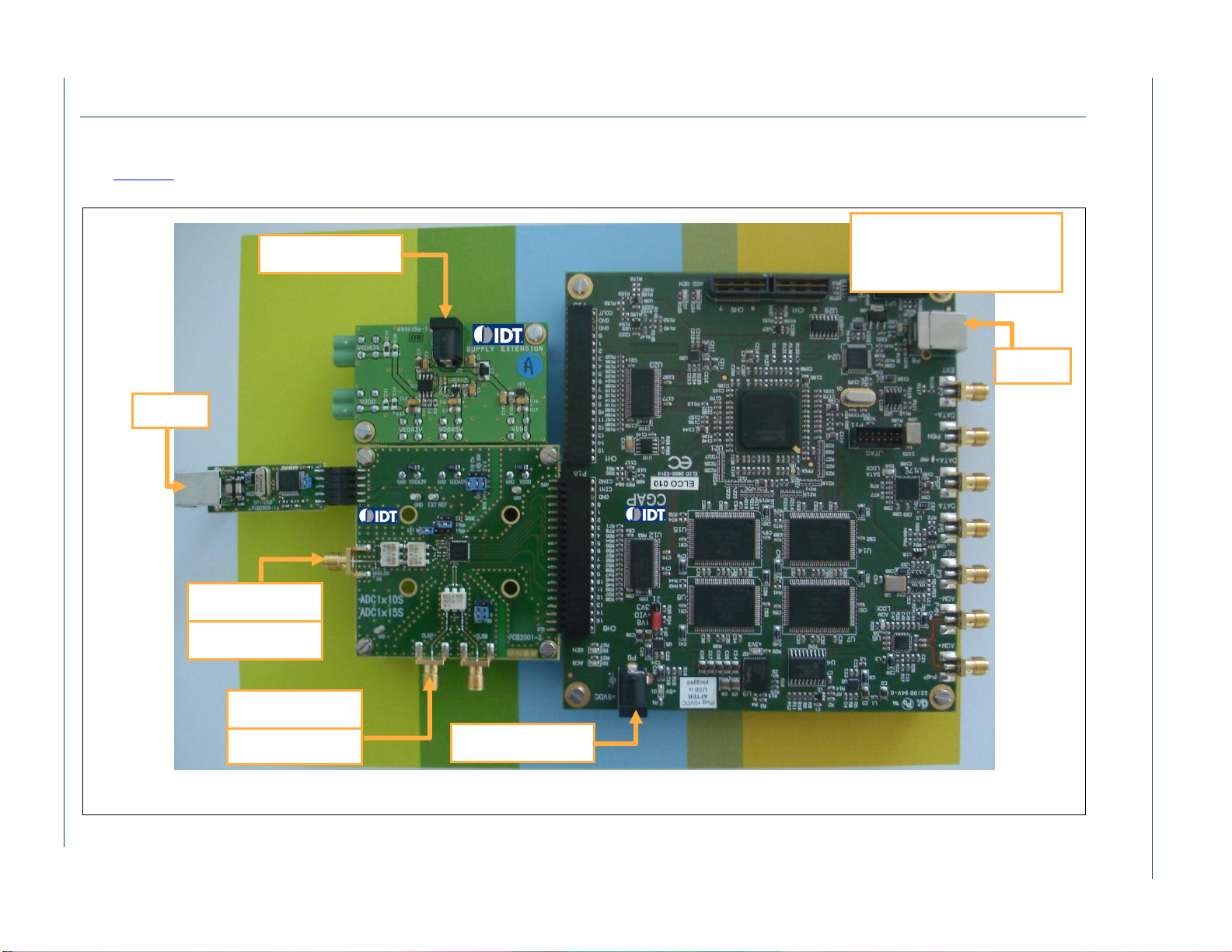
3. Combo ADC1410S and HSDC extension module
3.1 ADC1410S CMOS outputs
The figure 24 below shows an overview of the whole system ADC1410S+HSDC extension module with CMOS outputs configuration for which
connection is straightforward, together with a supply extension module (release A) for the ADC1410S demo-board:
Fig 6. Evaluation set-up measurement with ADC1410S CMOS and HSDC extension module
USB SPI
MODULE
PRESENTED CONFIGURATION
. Single-ended clock on CLKP
. 2Vpp input full scale
. Binary CMOS outputs
CLOCK SIGNAL
. e.g 122.88MHz
CLOCK
GENERATOR
REFERENCE SIGNAL
. e.g 170MHz
SIGNAL
GENERATOR
+5V POWER SUPPLY
. I = 3.2A
USB SPI
MODULE
+5V POWER SUPPLY
. I = 3.2A

Integrated Device Technology
Quick start ADC1410S, ADC1210S, ADC1010S series
Quick start
© IDT 2012. All rights reserved.
Quick start
Rev. 06 —2 July 2012
13 of 27
3.2 ADC Software tool
Run the application “SW_ADC_1_r02.exe”. This application will allow:
the user to control features on our high speed ADC through the SPI interface
available on any ADC1410S, ADC1210S and ADC1010S series;
As well as performing any online data acquisition to evaluate the performances of
the ADC1410S, ADC1210S and ADC1010S series.
At start-up, the program will detect any board connected to your system and display
information as can be seen on following window:
Fig 7. SW_ADC_1_r02: start-up screen
: “IDT Banner Button” will display your default internet browser to the IDT data
converter home page;
: “REFRESH” allows you to poll your system for any hardware change. It will reset any
board connected to your system;
: “QUIT” allows you quit the application;
: “INITIALIZATION” allow you to initialize the HSDC-EXTMOD board prior to any
acquisition task.
In the example above, the HSDC-EXTMOD has been detected, as well as
ADC1010S125.
At this moment, make sure that 4 LEDs are visible on the HSDC-EXTMOD (2 close to
power plug, 1 for USB and 1 close to FPGA).
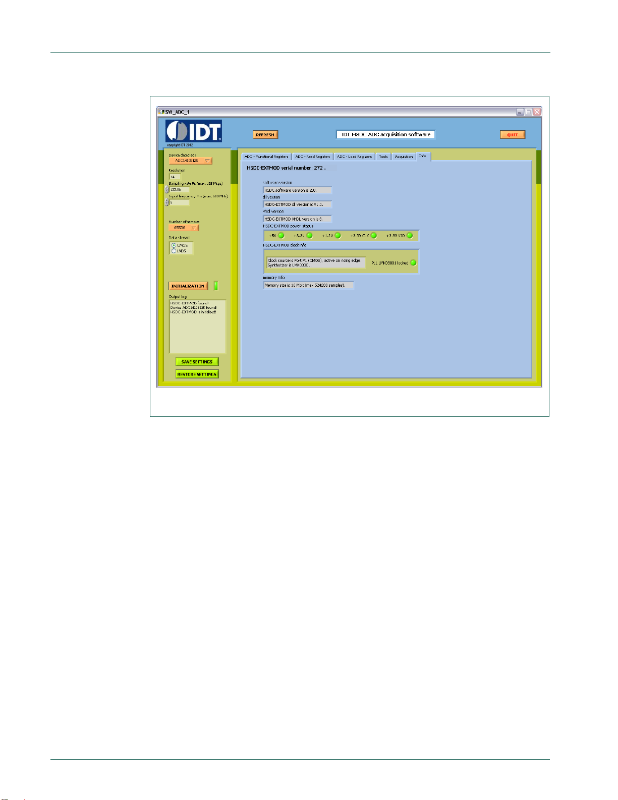
The “Info” page gives more details on the current hardware configuration for the HSDC-
EXTMOD board:
Integrated Device Technology
Quick start ADC1410S, ADC1210S, ADC1010S series
Quick start
© IDT 2012. All rights reserved.
Quick start
Rev. 06 —2 July 2012
14 of 27
Fig 8. SW_ADC_1_r02: “Info” page
The HSDC-EXTMOD is not yet initialized, so the embedded PLL (LMK03001 in this
example) is not locked. Initialization is only required for acquisition purpose.

Integrated Device Technology
Quick start ADC1410S, ADC1210S, ADC1010S series
Quick start
© IDT 2012. All rights reserved.
Quick start
Rev. 06 —2 July 2012
15 of 27
3.2.1 ADC SPI programming Functional Registers page
The page displays all SPI registers for ADC1410S, ADC1210S and ADC1010S series:
Fig 9. SW_ADC_1_r02: “ADC - Functional Registers” page
Perform any settings and then click on the “Send data to device” button to update the
device registers.

Integrated Device Technology
Quick start ADC1410S, ADC1210S, ADC1010S series
Quick start
© IDT 2012. All rights reserved.
Quick start
Rev. 06 —2 July 2012
16 of 27
3.2.2 ADC SPI programming Read Registers page
This page can be used to read all registers by clicking on the “Read all registers” button
and will display the result in the table below:
Fig 10. SW_ADC_1_r02: “ADC - Read Registers” page
When all registers have been read, it is possible to save the data to a text file. The
settings are saved in a table-like format as shown below:
Table 5. Typical saving on text file
Content of file is shown as table format
Column 1
Column 2
Address
Value
05
00
06
01
08
00
10
03
11
00
12
09
13
00
14
00
15
00
16
00
17
00

Integrated Device Technology
Quick start ADC1410S, ADC1210S, ADC1010S series
Quick start
© IDT 2012. All rights reserved.
Quick start
Rev. 06 —2 July 2012
17 of 27
Column 1
Column 2
20
0e
21
00
22
00
Note that all data are saved in hexadecimal format.
Click on the “Save registers read to file” button to select the file to store data to. Make
sure that you store your file with “.txt” extension, this will allow you to re-use the file on
the “ADC - Load Registers” page.
3.2.3 ADC SPI programming Load Registers page
This page allows downloading configuration data to the device registers:
Fig 11. SW_ADC_1_r02: “ADC - Load Registers” page
It is not necessary to have a file that has the whole set of registers listed. The only
restriction is regarding the formatting of the file as given in section 3.3.2.
Note: this page can not be used to download data saved during the comparison process.
To download settings onto device registers, follow the procedure below:
Browse to select your file (button );
Click on “Load data” button .
A message on field and a progress bar will inform about the status of the operation
until message “download done!” is seen. The table is updated with the current
values downloaded at the fly as can be seen on figure 13.

Integrated Device Technology
Quick start ADC1410S, ADC1210S, ADC1010S series
Quick start
© IDT 2012. All rights reserved.
Quick start
Rev. 06 —2 July 2012
18 of 27
3.2.4 Tools page
This page allows the user to calculate the coherent frequencies values involved of the
acquisition process. It gives an indication where the 6 first harmonics are located in
the Nyquist zone.
Enter your analog and sampling frequencies in field.Indicate the number of
samples to be acquired, as well as the fixed parameter for the coherency
calculation (Fs in our example above). Press “UPDATE GRAPH” to look at the
frequency plan, it gives also the real Fin frequency (Refer to appendix A.1 for more
details on coherency calculation):
Fig 12. SW_ADC_1_r02: “Tools” page
Note: The level of the harmonics shown does not reproduce the behavior of the ADC;
they are only given as indication for location.

Integrated Device Technology
Quick start ADC1410S, ADC1210S, ADC1010S series
Quick start
© IDT 2012. All rights reserved.
Quick start
Rev. 06 —2 July 2012
19 of 27
3.2.5 Acquisition page
This page will acquire data to evaluate the high dynamic performance of the device:
Fig 13. SW_ADC_1_r02: “Acquisition” page
Before proceeding to any acquisition, the user needs to do the following entries:
the sampling frequency Fs: 80 Msps in our example (field );
the input frequency Fin: 175 MHz in our example for both ADC channels (field );
the number of samples to be acquired 16384 in our example (field );
indicate whether it is CMOS or LVDS DDR (field );
press the “INITIALIZATION” button . It will initialized the HSDC-EXTMOD
board:
FPGA is ready (red LED is flashing ¼ on and ¾ off) ;
PLL embedded is locked (green LED is on);
indicate whether Fin or Fs are coherent or not (field ):
if signals are coherent, selected which Fin or Fs are fixed for the calculation
(see appendix A.1);
if signals are not coherent, select the window for FFT processing to apply (the
Blackman window gives better results).
press the “ACQUIRE” button to display the results from the FFT processing.
The results fields will be updated automatically depending on the display
choice using the “Display …” button (“Display ADC0” or “Display ADC1” or
“Display ADC0 & ADC1”).
press “STOP” button to stop acquisition;
field allows to do FFT averaging over up to 255 trials, suitable for small signal
analysis;

Integrated Device Technology
Quick start ADC1410S, ADC1210S, ADC1010S series
Quick start
© IDT 2012. All rights reserved.
Quick start
Rev. 06 —2 July 2012
20 of 27
field allows to store dynamic results to text file. Click on the check box, enter a
header as a comment and browse to indicate where to store data file. Table 7
shows how data are stored:
Table 6. Dynamic results as stored in a text file
Content of file is shown as table format
Name
Fin
Fs
Vin
ENOB
SINAD_C
SNR_C
SNR_FS
SFDR_C
SFDR_FS
THD
H2
H3
H4
H5
H6
(MHz)
(MHz)
(dBFS)
-
(dBc)
(dBc)
(dBFS)
(dBc)
(dBFS)
(dBc)
(dBc)
(dBc)
(dBc)
(dBc)
(dBc)
ADC1410S test
ADC0
5.00
122.88
-0.96
11.28
69.79
69.67
70.75
84.62
85.58
-85.27
-104.62
-100.12
-103.67
-86.57
-112.78
Note that ADC0 and ADC1 refer to the acquisition path on the HSDC-EXTMOD
board. It corresponds respectively to the bottom and top ADC of the ADC1410S,
ADC1210S and ADC1010S series.
Note that while acquisition is running, any other action (ADC SPI programming, quit or
refresh) is not possible. Stop acquisition first before proceeding to any other task.
3.2.5.1 FFT spectrum
The first graph to be displayed is the FFT spectrum of the digital pattern acquired:
Fig 14. SW_ADC_1_r02: “Acquisition” page, FFT graph
Press the “Autoscale” button to display the whole content.
This manual suits for next models
2
Table of contents
Other IDT Motherboard manuals


IDT
IDT EVK-UFT285-6-7 User manual

IDT
IDT Tsi382 LQFP User manual

IDT
IDT 9FGV1005 Operating instructions

IDT
IDT P9241-G-EVK User manual

IDT
IDT P9242-R-EVK User manual

IDT
IDT ZSSC41 Series User manual

IDT
IDT ZNRG2061 User manual

IDT
IDT EB8T5A Eval Board User manual

IDT
IDT 9ZXL1951D User manual

IDT
IDT Tsi84 User manual


