IDT VersaClock 5 User manual
USER GUIDE
REVISION A 05/13/15 1 ©2015 Integrated Device Technology, Inc.
VersaClock®5 - 5P49V5935/33 Evaluation Boards
Introduction
The evaluation board is designed to help the customer evaluate the 5P49V5935/33, the latest addition to the family of
programmable devices in IDT's Timing portfolio. When the board is connected to a PC running IDT Timing Commander™
Software through USB, the device can be configured and programmed to generate frequencies with best-in-class performances.
Board Overview
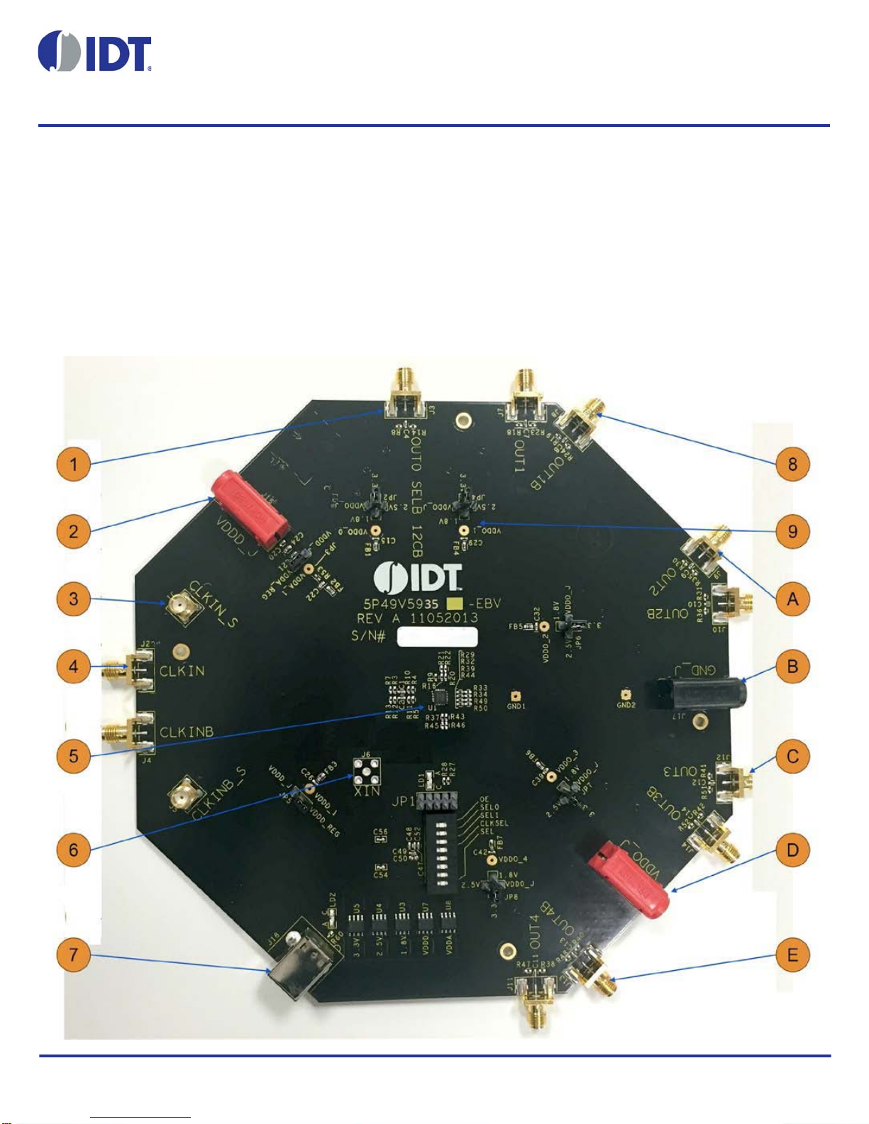
Use the following diagram to identify: power supply jacks, USB connector, input and output frequency SMA connectors.
Figure 1. Board Overview

2 REVISION A 05/13/15
VERSACLOCK®5 - 5P49V5935/33 Evaluation Boards
OUT0 - This is a buffered output of the input reference clock, singled ended.
Power supply jack, J16 – Connect to 3.3V, 2.5V or 1.8V for the core voltage of the device.
CLKIN_S/CLKINB_S – SMA pair used to monitor the differential input CLKIN/CLKINB.
Differential Input clock connector – A differential clock can be connected as a source for the device.
5P49V5935/33 – the device to be evaluated.
XIN Connector – This SMA connector is for single-ended clock input. Please note the full swing of this input is 1.2V
maximum.
USB connector – Used this connector to connect with your PC to run IDT Timing Commander Software.
OUT1 /OUT1B – Output 1. It can be a differential pair or two individual single-ended outputs. By default, it's an LVPECL
differential output.
Output voltage selector – 4-way header to select an output voltage. The center pin is the output voltage. Use the jumper
to select from 1.8V, 2.5V or 3.3V. VDDO_J is the voltage from J15 (see E).
OUT2/OUT2B – Output 2. It can be a differential pair or two individual single-ended outputs. By default, it's an LVPECL
differential output.
Ground Jack – J17. If J15 and/or J16 is used for power supply, this jack is the power return.
OUT3/OUT3B – Output 3. It can be a differential pair or two individual single-ended outputs. By default, it's an LVPECL
differential output. (OUT3/OUT3B is not populated on 5P49V5933 EVB.)
Output Voltage Jack – J15. Connect to a voltage of 1.8V, 2.5V or 3.3V for output voltages.
OUT4/OUT4B – Output 4. It can be a differential pair or two individual single-ended outputs. By default, it's an LVPECL
differential output. (OUT4/OUT4B is not populated on 5P49V5933 EVB.)
Board Power Supply
• Core Voltages
The core voltage includes a digital voltage VDDD and an analog voltage VDDA. Both core voltages can be powered by an
external bench power supply or by USB.
Bench Power Supply – To supply VDDD with a bench power supply, connect power to J16. To supply VDDA with a bench power
supply, connect power to J15. In the same time, place the jumpers in JP3 and JP5 to connect VDDA_J and VDDD_J, respectively.
USB Power Supply – When the board is connected to a PC through a USB cable, on-board voltage regulators will generate a
3.3V for the device. In this case, place the jumpers in JP3 and JP5 to connect VDDA_REG and VDDD_REG, respectively. See
JP5 jumper position for VDDD_REG in the following figure. USB power source is recommended because it's readily available
right from your laptop.
1
2
3
4
5
6
7
8
9
A
B
C
D
E
REVISION A 05/13/15 3
VERSACLOCK®5-5P49V5935/33EvaluationBoards
Figure 2. Jumping to the VDDD_J side will select external bench power supply; Jumping to the VDD_REG
side will select power source from on-board regulators powered by USB
• Output Clock Voltages
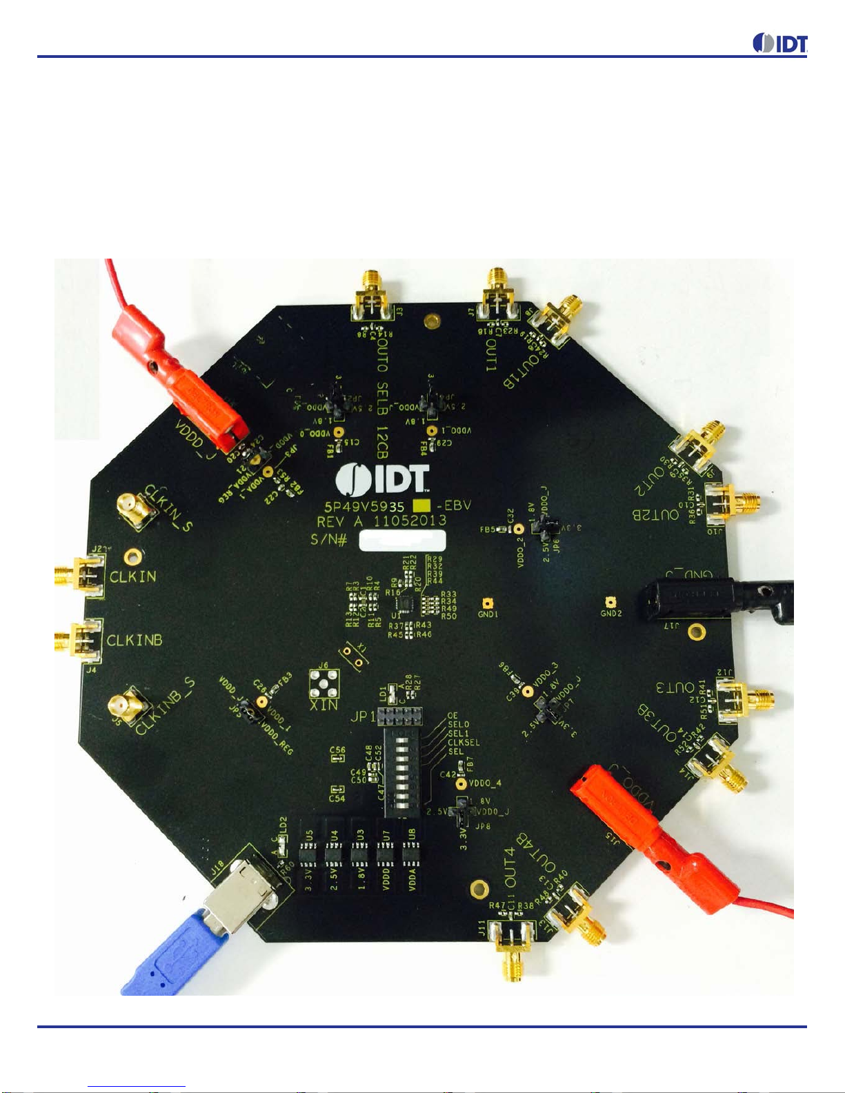
Like VDDA and VDDD having two sources, each output voltage VDDO0~4 is also provided with two sources to choose from:
bench power supply or powered from USB. The selection is made by a 4-way header as shown in Figure 3 below. Jumping to
VDDO_J will select external power supply (JP15 and JP16 are connected to external power supply); Jumping to 1.8V, 2.5V or
3.3V will select each respective voltage from on-board voltage regulators powered by USB port.
Please note: each output voltage can be individually selected. Use the label on the evaluation board: VDDO_0 for OUT0,
VDDO_1 for OUT1, VDDO_2 for OUT2, VDDO_3 for OUT3, and VDDO_4 for OUT4 (5P49V5933 has only two outputs –
OUT1/OUT1B and OUT2/OUT2B whereas, 5P49V5935 has 4 outputs – OUT1/OUT1B, OUT2/OUT2B, OUT3/OUT3B and
OUT4/OUT4B).
Figure 3. Use the jumper to select a voltage for OUT3: 1.8V/2.5V/3.3V is from on-board voltage regulators
powered by USB; VDDO_J is from external power supply connecting to JP15 and JP16
4 REVISION A 05/13/15
VERSACLOCK®5 - 5P49V5935/33 Evaluation Boards
Connecting the Board
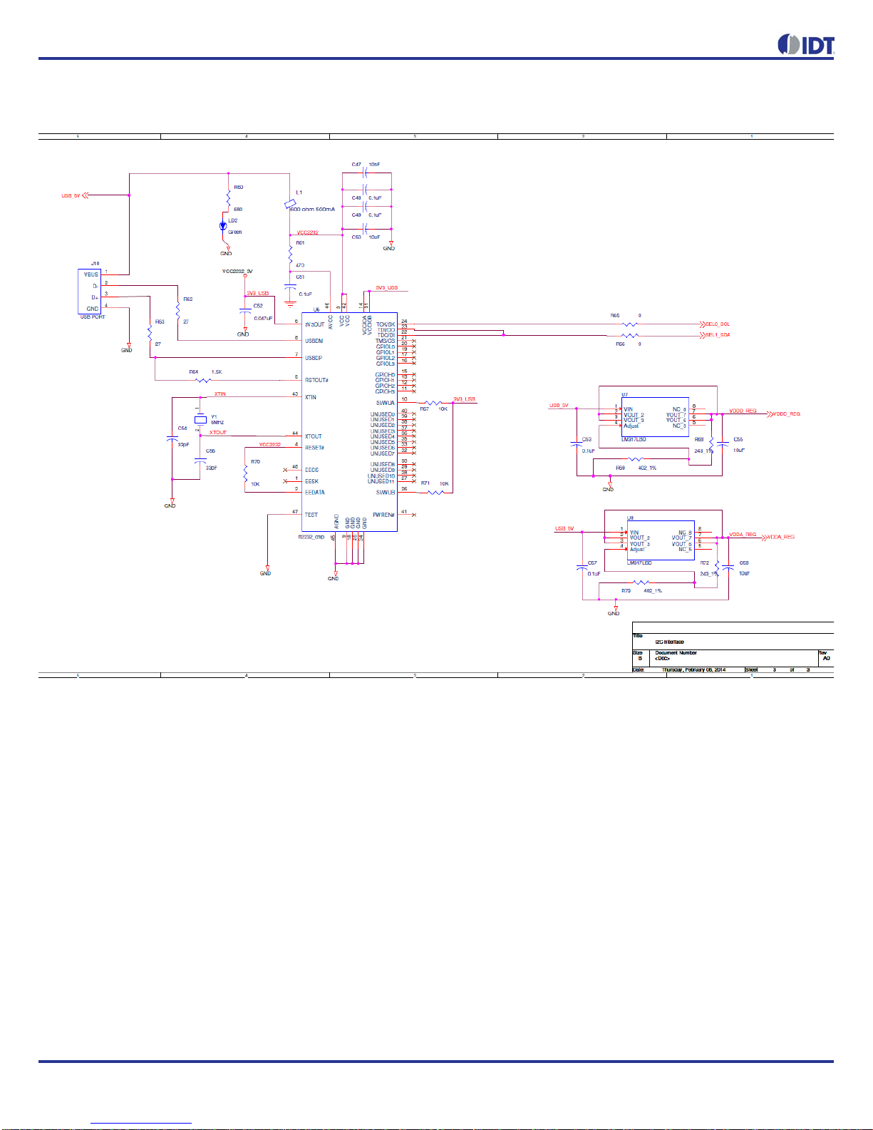
The board is connected to a PC through a USB connector for configuring and programming the device, as shown in Figure 4
below. The USB interface will also provide +5V power supply to the board, from which on-board voltage regulators generate
various voltages for the core as well as for each output.
The board can also be powered by a bench power supply by connecting two banana jacks J15, J16 for output and core voltages,
respectively. Please see board power supply section for details.
Figure 4. Connecting the Board with USB Port for Communications with Timing Commander Software

REVISION A 05/13/15 5
VERSACLOCK®5-5P49V5935/33EvaluationBoards
Configuration and Setup
The 5P49V5935/33 EVB do not need an on board crystal since it is integrated inside the device. An external clock can still be
supplied to CLKIN/CLKINB connectors. The device will have two default outputs: OUT0 = 25MHz, OUT1 =100MHz when
powered up.
Use the following steps to setup the board using I2C and start the configuration of the board.
1. Set SEL pin (pin 8) of dip switch (U2) to "0" to select I2C mode.
2. Connect J18 to a USB port of the PC using the supplied I2C cable.
3. Power up the board.
4. Launch Timing Commander Software (refer to VersaClock5 Timing Commander User Guide - Getting Started Step 1~7).
Following the Getting Started steps in the Timing Commander software, an I2C connection is established between the GUI
software and chip.
5. First load the personality file 1.30 and select 5P49V5933 or 5P49V5935 part number, then load the setting file into the GUI
and start configuring the IC.
6. All intended outputs should be available for measurement.
Board Schematics
Evaluation board schematics are shown on the following pages.

6 REVISION A 05/13/15
VERSACLOCK®5 - 5P49V5935/33 Evaluation Boards
Figure 5. VersaClock 5 Evaluation Board Schematics – Page 1

REVISION A 05/13/15 7
VERSACLOCK®5-5P49V5935/33EvaluationBoards
Figure 6. VersaClock 5 Evaluation Board Schematics – Page 2
8 REVISION A 05/13/15
VERSACLOCK®5 - 5P49V5935/33 Evaluation Boards
Figure 7. Evaluation Board Schematics – Page 3
REVISION A 05/13/15 9
VERSACLOCK®5-5P49V5935/33EvaluationBoards
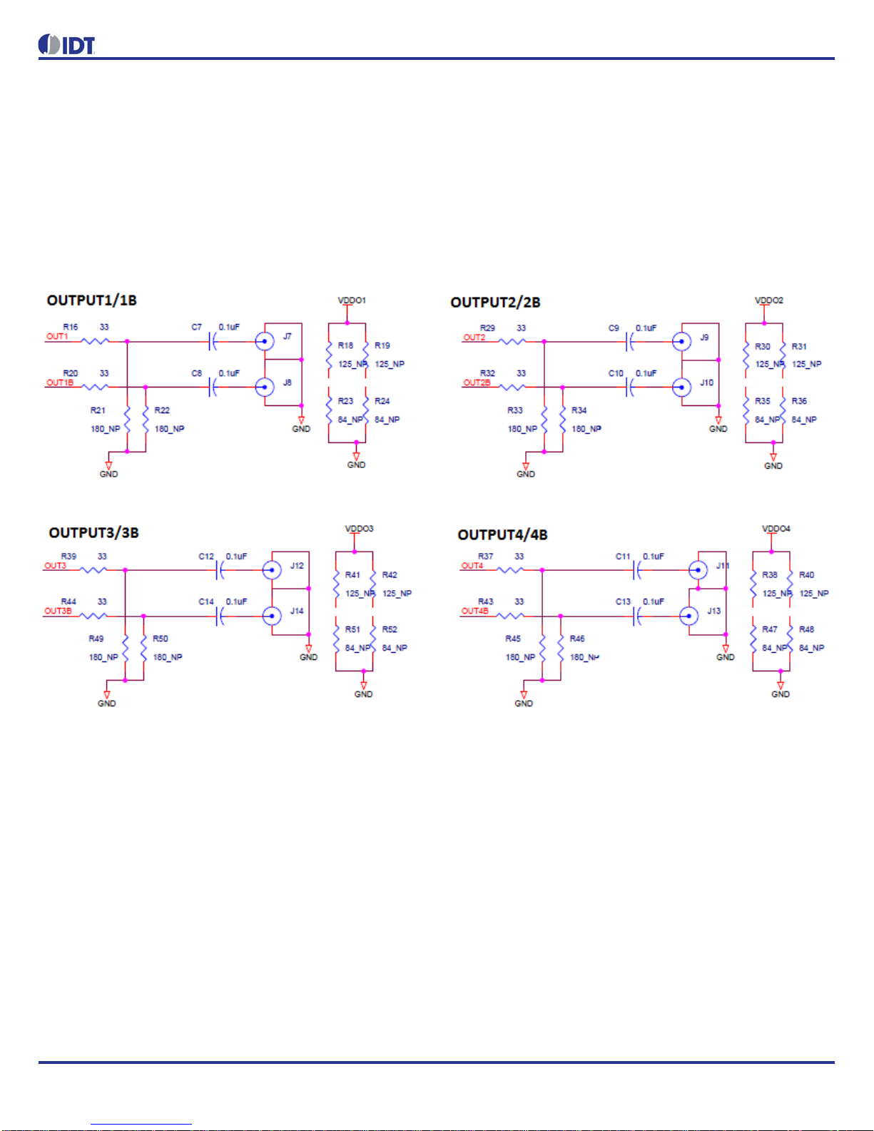
Signal Termination Options
Termination options for OUTPUT1 – 4 in the evaluation board are displayed in Figure 8. The termination circuits are designed to
optionally terminate the output clocks in LVPECL, LVDS, LVCMOS and HCSL signal types by populating (or not-populating)
some resistors. DC or AC coupling of these outputs are also supported.
Tables1 – 2, below, tabulates component installations to support LVPECL, HCSL, LVCMOS and LVDS signal types for OUTPUT1
– 4, respectively. Please note that by doing so, the output signals will be measured and terminated by an oscilloscope with a 50
internal termination.
Figure 8. Output Termination Options
10 REVISION A 05/13/15
VERSACLOCK®5 - 5P49V5935/33 Evaluation Boards
Table 1. 5P49V5933 EVB Output Termination
Table 2. 5P49V5935 EVB Output Termination
Orderable Part Numbers
The following evaluation board part numbers are available for order.
Table 3. Orderable Part Numbers
Output Number Signal Type Series Resistors 180-ohm pull-down Series Capacitor Resistor Network
OUTPUT1 LVPECL R16=R20=0 R21, R22 installed C7=C8=0.1 µF R18, R19, R23, R24
not installed
OUTPUT2 LVDS R29=R32=0 R33, R34 not installed C9=C10=0.1 µF R30, R31, R35, R36
not installed
Output Number Signal Type Series Resistors 180-ohm pull-down Series Capacitor Resistor Network
OUTPUT1 HCSL R16=R20=33 R21, R22 not installed C7=C8=0 µF R18, R19, R23, R24
not installed
OUTPUT2 LVDS R29=R32=0 R33, R34 not installed C9=C10=0.1 µF R30, R31, R35, R36
not installed
OUTPUT3 LVPECL R39=R44=0 R49, R50 installed C12=C14=0.1 µF R41, R42, R51, R52
not installed
OUTPUT4 LVCMOS R37=R43=33 R45, R46 not installed C11=C13=0.1 µF R38, R40, R47, R48
not installed
Part Number Description
EVKVC5-5935ALL Evaluation board for 5P49V5935. Output termination configurations are described in Table 2.
EVKVC5-5933ALL Evaluation board for 5P49V5933. Output termination configurations are described in Table 1.

DISCLAIMER Integrated Device Technology, Inc. (IDT) and its subsidiaries reserve the right to modify the products and/or specifications described herein at any time and at IDT’s sole discretion. All information in
this document, including descriptions of product features and performance, is subject to change without notice. Performance specifications and the operating parameters of the described products are determined
in the independent state and are not guaranteed to perform the same way when installed in customer products. The information contained herein is provided without representation or warranty of any kind, whether
express or implied, including, but not limited to, the suitability of IDT’s products for any particular purpose, an implied warranty of merchantability, or non-infringement of the intellectual property rights ofothers. This
document is presented only as a guide and does not convey any license under intellectual property rights of IDT or any third parties.
IDT’s products are not intended for use in applications involving extreme environmental conditions or in life support systems or similar devices where the failure or malfunction of an IDT product can be reasonably
expected to significantly affect the health or safety of users. Anyone using an IDT product in such a manner does so at their own risk, absent an express, written agreement by IDT.
Integrated Device Technology, IDT and the IDT logo are registered trademarks of IDT. Product specification subject to change without notice. Other trademarks and service marks used herein, including protected
names, logos and designs, are the property of IDT or their respective third party owners.
Copyright ©2015 Integrated Device Technology, Inc.. All rights reserved.
Corporate Headquarters
6024 Silver Creek Valley Road
San Jose, CA 95138 USA
Sales
1-800-345-7015 or
408-284-8200
Fax: 408-284-2775
www.IDT.com
Tech Support
email: [email protected]
480-763-2056
This manual suits for next models
2
Table of contents
Other IDT Motherboard manuals

IDT
IDT P9242-G-EVK User manual

IDT
IDT ZSSC41 Series User manual

IDT
IDT ZMOD4510-EVK User manual

IDT
IDT ZMID520 Series User manual

IDT
IDT 82P33731 User manual

IDT
IDT Tsi340-RDK1 User manual

IDT
IDT 9ZXL1951D User manual

IDT
IDT VersaClock 6E 5P49V6965 User manual

IDT
IDT Tsi381 User manual

IDT
IDT ZSSC4151 User guide

IDT
IDT EB-LOGAN-23 User manual

IDT
IDT 82P33714 User manual

IDT
IDT ADC1410S Series User manual

IDT
IDT 89EBPES16NT2 User manual

IDT
IDT P9221-R-EVK User manual

IDT
IDT VersaClock 3S User manual

IDT
IDT 8T49N240 User manual

IDT
IDT 89EB-LOGAN-19 User manual

IDT
IDT 89EBPES24T3G2 User manual

IDT
IDT 82V3911 User manual


