IDT 89EBPES48H12 User manual

January 2007
6024 Silver Creek Valley Road, San Jose,California 95138
Telephone: (800) 345-7015 • (408) 284-8200 • FAX: (408) 284-2775
Printed in U.S.A.
©2007 Integrated Device Technology, Inc.
IDT™89EBPES64H16 /
89EBPES48H12 / 89EBPES48T12
Evaluation Board Manual
(Eval Board: 18-624-000)

DISCLAIMER
Integrated Device Technology, Inc. reserves the right to make changes to its products or specifications at any time, without notice, in order to improve design or performance
and to supply the best possible product. IDT does not assume any responsibility for use of any circuitry described other than the circuitry embodied in an IDT product. The
Company makes no representations that circuitry described herein is free from patent infringement or other rights of third parties which may result from its use. No license is
granted by implication or otherwise under any patent, patentrights or other rights, of Integrated Device Technology, Inc.
Boards that fail to function should be returned to IDT for replacement. Credit will not be given for the failed boards nor will a
Failure Analysis be performed.
LIFE SUPPORT POLICY
Integrated Device Technology's products are not authorized for use as critical components in life support devices or systems unlessa specific written agreementpertaining to
such intended use is executed between the manufacturer and an officer of IDT.
1. Life support devices or systems are devices or systems which (a) are intended for surgical implant into the body or (b) support or sustain life and whose failure to perform,
when properly used in accordance with instructions for use providedin the labeling, can be reasonably expected toresult in a significant injury to the user.
2.A criticalcomponentisany componentsof alifesupportdeviceor systemwhosefailure toperformcanbe reasonablyexpected to cause the failure of the life support device
or system, or to affect its safety or effectiveness.
IDT,the IDT logo, and Integrated Device Technologyare trademarks or registered trademarks of Integrated Device Technology, Inc.

Notes
EB64H16 Eval Board Manual i January 16, 2007
Table of Contents
Description of the EB64H16 Eval Board
Foreword.........................................................................................................................................1-1
Introduction.....................................................................................................................................1-1
Board Features...............................................................................................................................1-3
Feature List.............................................................................................................................1-3
Performance Summary...................................................................................................................1-3
Software..................................................................................................................................1-4
Other.......................................................................................................................................1-4
Revision History..............................................................................................................................1-4
Installation of the EB64H16 Eval Board
EB64H16 Installation ......................................................................................................................2-1
PCI Express Adapter Card..............................................................................................................2-1
Hardware Description .....................................................................................................................2-2
Host System...........................................................................................................................2-2
Reference Clocks............................................................................................................................2-3
Power Sources................................................................................................................................2-6
Power Supply Minimum Load Connectors..............................................................................2-7
PCI Express Serial Data Transmit Termination Voltage Converter........................................2-8
PCI Express Digital Power Voltage Converter........................................................................2-8
PCI Express Analog Power Voltage Converter......................................................................2-8
Core Logic Voltage Converter................................................................................................2-8
3.3V I/O Power Module...........................................................................................................2-8
Power-up Sequence...............................................................................................................2-8
Required Jumpers..................................................................................................................2-8
Heatsink Requirement....................................................................................................................2-8
Reset...............................................................................................................................................2-8
Fundamental Reset................................................................................................................2-9
Downstream Reset.................................................................................................................2-9
Boot Configuration Vector.............................................................................................................2-10
SMBus Interfaces..........................................................................................................................2-12
SMBus Slave Interface.........................................................................................................2-12
SMBus Master Interface.......................................................................................................2-13
JTAG Header................................................................................................................................2-14
Attention Buttons...........................................................................................................................2-14
Miscellaneous Jumpers, Headers.................................................................................................2-15
LEDs.............................................................................................................................................2-18
PCI Express Connectors...............................................................................................................2-21
PCI Express Personality Module ..................................................................................................2-23
EB64H16 Evaluation Board Block Diagram..................................................................................2-24
Software for the EB64H16 Eval Board
Introduction.....................................................................................................................................3-1
Device Management Software........................................................................................................3-1
Schematics
Schematics.....................................................................................................................................4-1

IDT Table of Contents
EB64H16 Eval Board Manual ii January 16, 2007
Notes

Notes
EB64H16 Eval Board Manual iii January 16, 2007
List of Tables
Table 2.1 Clock Source Selection .......................................................................................................2-3
Table 2.2 Clock Frequency Selection .................................................................................................2-4
Table 2.3 Clock Spread Spectrum Selection ......................................................................................2-4
Table 2.4 SMA Connectors - Onboard Reference Clock ....................................................................2-4
Table 2.5 EPS12V 24_pin Power Connector - J6 ...............................................................................2-7
Table 2.6 EPS12V 8-Pin Connector - J5 ............................................................................................2-7
Table 2.7 Minimum Load Connectors .................................................................................................2-7
Table 2.8 Downstream Reset Selection .............................................................................................2-9
Table 2.9 Boot Configuration Vector Signals ....................................................................................2-10
Table 2.10 Boot Configuration Vector Switches S19, S20 & S21 (ON=0, OFF=1) ............................2-11
Table 2.11 Slave SMBus Interface Connector ....................................................................................2-12
Table 2.12 SMBus Slave Interface Address Configuration .................................................................2-12
Table 2.13 PES64H16 SMBus Slave Interface Address Setting ........................................................2-13
Table 2.14 EEPROM SMBus Address Setting ...................................................................................2-13
Table 2.15 JTAG Connector Pin Out ..................................................................................................2-14
Table 2.16 Attention Buttons ..............................................................................................................2-14
Table 2.17 Miscellaneous Jumpers, Headers .....................................................................................2-15
Table 2.18 LED Indicators ..................................................................................................................2-18
Table 2.19 PCI Express x16 Connector Pinout ..................................................................................2-21
Table 2.20 PES64H16 Personality Module Locations ........................................................................2-23

IDT Table of Contents
EB64H16 Eval Board Manual iv January 16, 2007
Notes

Notes
EB64H16 Eval Board Manual v January 16, 2007
List of Figures
Figure 1.1 Functional Block Diagram of the EB64H16 Eval Board .....................................................1-2
Figure 1.2 Functional Block Diagram of the EB48H12 and EB48T12 Eval Boards ............................1-2
Figure 2.1 PCIe Adapter .....................................................................................................................2-1
Figure 2.2 SuperMicro X6DH8-G2 Motherboard .................................................................................2-3
Figure 2.3 Clock Distribution Block Diagram .......................................................................................2-5
Figure 2.4 Power Distribution Block Diagram ......................................................................................2-6
Figure 2.5 EB64H16 Eval Board Block Diagram ...............................................................................2-24
Figure 2.6 EB48H12 / EB48T12 Eval Board Block Diagram .............................................................2-25

IDT List of Figures
EB64H16 Eval Board Manual vi January 16, 2007
Notes

Notes
EB64H16 Eval Board Manual 1 - 1 January 16, 2007
Chapter 1
Description of the EB64H16
Eval Board
Foreword
This evaluation board manual includes hardware and software information on the 89HPES64H16,
89HPES48H12, and 89HPES48T12 peripheral chips. All three devices are members of IDT’s PRECISE™
family of PCI Express® switching solutions.
The 89HPES64H16 (PES64H16) is a 64-lane, 16-port switch and the 89HPES48H12 (PES48H12) is a
48-lane, 12-port switch. Both devices are system interconnect switches that perform PCI Express packet
switching with a feature set optimized for high-performance applications where multiple peer-to-peer traffic
flows are simultaneously transmitted.
The 89HPES48T12 (PES48T12)is a 48-lane, 12-port peripheral chip that performs PCI Express Packet
switching with a feature set optimized for high-performance applications such as servers, storage, and
communications/networking.
The same evaluation board is used for all three of these devices and, consequently, the information in
this manual applies equally, with some exceptions, to all three devices. Throughout the manual, numerous
references are made to the 89EBPES64H16 Evaluation Board (also referred to as EB64H16). These refer-
ences to the EB64H16 should be interpreted as also applying to both an EB48H12 board and an EB48T12
board, except where noted.
Introduction
The EB64H16 evaluation board provides an evaluation platform for the PES64H16 switch. The
EB64H16 has two x4 ports which can be merged to provide one x8 upstream port on a standard x16 PCI
Express connector. This port is used to connect an adaptorcard with a cable to another adaptor card in the
root complex or host system. Alternatively, the upstream port can be defined as a x4 port allowing for fifteen
downstream ports.
The downstream slots will conform to the x8 and x4 connector pin assignments but will be populated
with x16 connectors. The unused lane bits on the x16 connectors will be unconnected. The core and IO
power for the PES64H16 is derived from the 12V power supply connector from a 12VEPS type power
supply with a 24-pin connector and a 8-pin connector with 12V. The downstream slot power is controlled
through hot-plug controllers with power provided from the 12VEPS power supply connector with 12V. A
personality module is used to optionally merge two x4 ports into one x8 downstream port connector. The
PES64H16 Evaluation board block diagram is shown in Figure 1.1 and the PES48H12 / PES48T12 block
diagram is shown in Figure 1.2.

IDT Description of the EB64H16 Eval Board
EB64H16 Eval Board Manual 1 - 2 January 16, 2007
Figure 1.1 Functional Block Diagram of the EB64H16 Eval Board
Figure 1.2 Functional Block Diagram of the EB48H12 and EB48T12 Eval Boards
25MHz
SSC
Clock
Clock
Fanout
JTAG
Header
Reset
IDT
64 Lanes / 16 Ports
USPCTL
Header
Slave
SMBus
Master
SMBus
EEPROM
IO EXPs
P. M.
P5P4
P7
P6
Downstream x4
Upstream x8
P1
P0
P. M.
Downstream x4
P3
P2
Downstream x4
P. M.
Downstream x4
Downstream x4
P. M.
Downstream x4
Downstream x4
P. M.
Downstream x4
Downstream x4
P. M.
Downstream x4
Downstream x4
P. M.
Downstream x4
Downstream x4
P. M.
Downstream x4
Downstream x4
P15 P8 P9
P14 P13
P12 P11
P10
25MHz
SSC
Clock
Clock
Fanout
JTAG
Header
Reset
IDT
48 Lanes / 12 Ports
USPCTL
Header
Slave
SMBus
Master
SMBus
EEPROM
IO EXPs
P. M. P. M. P. M. P. M.
Downstream x8
Downstream x4
Downstream x8
Downstreamx4
Downstreamx8
Downstream x4
P5
P4
P7
P6
P9P8
Downstream x4
Upstreamx8
P1
P0
P. M.
Downstream x8
Downstream x4
P3
P2
P. M.
Downstream x8
Downstream x4
P11P10

IDT Description of the EB64H16 Eval Board
EB64H16 Eval Board Manual 1 - 3 January 16, 2007
Notes Board Features
Feature List
The EB64H16 has one x8 PCI Express upstream port to the root complex provided by a PCI
Express adaptor board to a cable that connects to another adaptor board in the root complex or
host system.
The EB64H16 provides fifteen downstream connectors with x4 ports, while the EB48H12 and
EN48T12 provide 11 downstream connectors. Two x4 downstream slots can be configured as one
x8 port through the personality modules.
All fifteen downstream slots for the PES64H16 and all eleven downstream slots for the PES48H12
and PES48T12 have hot-plug support through power isolation controlled by a hot-plug controller
and IO expanders on the Master SMBUS. The Master SMBUS is controlled by the PES64H16
through configuration registers.
The EB64H16 has a 12V to 2.5V DC-DC converter that uses the 12V power from an external
12VEPS power supply connector with 12V. The 2.5V provides power to the DC-DC converters for
the PES64H16 core power.
JTAG connector to the PES64H16 JTAG pins.
Serial EEPROM on the PES64H16 master SMBUS interface.
Provides an SMBUS connector on the PES64H16 slave SMBUS interface.
Has a fundamental cold and warm reset mechanism and a reset push button switch.
Provides a clock reference to the fifteen (or eleven) downstream ports from the upstream clock ref-
erence or from an on-board clock generator. The clock generator has spread spectrum clocking
option and SMA connectors are provided to monitor the clock.
Has LED displays to indicate power is applied, reset condition, port status, and downstream slot
power.
Has card present detect pins implemented on upstream and downstream slots.
Has ATTN push button switches and LED displays for each downstream slot.
Has a +12V fan connector for the integrated heatsink for the socket and soldered device.
Performance Summary
Provides up to 16 ports with 64 PCIe lanes (PES64H16) or up to 12 ports with 48 PCIe lanes
(PES48H12/PES48T12)
Integrated SerDes support 2.5 Gbps operation
Delivers up to 32 GBps (256 Gbps) of aggregate bandwidth
Sub 280ns latency through the switch
Supports two virtual channels
Compliant with PCI Express Base Specification Rev1.1 with Rev 2.0 features
Flexible Architecture with Numerous Configuration Options
Eight x8 PCIe ports
Each port can be independently bifurcated into two x4 PCIe ports
Supports automatic per port link width negotiation(e.g., x8/x4/x2/x1 for a x8 port)
Automatic lane reversal detection
Independent per port crosslink support
Supports lock transactions, allowing use of PCI Express with legacy software
Ability to load device configuration from serial EEPROM
Supports external signal for hot plug event notification allowing SCI/SMI generation for legacy oper-
ating systems
Supports external signal for power management event notification

IDT Description of the EB64H16 Eval Board
EB64H16 Eval Board Manual 1 - 4 January 16, 2007
Notes Software
There is no software or firmware executed on the board. However, useful software is provided along
with the Evaluation Board to facilitate configuration and evaluation of the PES64H16 within host systems
running popular operating systems.
Installation programs
–Operating Systems Supported: Windows2000, WindowsXP, Linux
GUI based application for Windows and Linux
–Allows users to view and modify registers in the PES64H16
–Binary file generator for programming the serial EEPROMs attached to the SMBUS
Other
An external power supply may be required under some conditions.
An SMBUS cable may be required for certain evaluation exercises.
SMA connectors are provided on the EB64H16 board for specific test points.
Revision History
January 16, 2007: Published production release board revision 0.9.
Notes
EB64H16 Eval Board Manual 2 - 1 January 16, 2007
Chapter 2
Installation of the EB64H16
Eval Board
EB64H16 Installation
This chapter discusses the steps required to configure and install the EB64H16 evaluation board. All
available DIP switches and jumper configurations are explained in detail. The primary installation steps are:
1. Configure jumper/switch options suitable for the evaluation or application requirements.
2. Connect PCI Express endpoint cards to the downstream port PCIe slots on the evaluation board.
3. Connect a PCI Express adapter card in an upstream port with a cable to another PCI Express
adaptor card in the root complex or host system, as shown in Figure 2.1.
4. Turn the power switch on the eval board (located at S3) to ON.
5. Apply power to the host system.
The EB64H16 board is shipped with all jumpers and switches configured to their default settings. In
most cases, the board does not require further modification or setup.
PCI Express Adapter Card
The PCI Express adapter card contains eight PCI Express lanes (see Figure 2.1). The lower four lanes
are routed to an Infiniband connector J2 and the upper four lanes to J3. The differential REFCLKp and
REFCLKn pins are routed to J5and J6, respectively. The JTAG interface and PERST# pins arerouted to J4
although only PERST# pin is actually used. Two PCI Express Adapter cards are required to connect the
EB64H16 evaluation board to the host PC and remember to match the connector connection between two
cards.
Figure 2.1 PCIe Adapter
4
4
4
4
REFCLKp
REFCLKn
Infiniband Cable
Infiniband Cable
PCIE Adapter Board
Install in HOST PC
PCIE Adapter Board
Install in 89EBPES64H16
Evaluation Board
PERST#
4
4
4
4
REFCLKp
REFCLKn
Infiniband Cable
Infiniband Cable
PCIE Adapter Board
Install in HOST PC
PCIE Adapter Board
Install in 89EBPES64H16
Evaluation Board
PERST#

IDT Installation of the EB64H16 Eval Board
EB64H16 Eval Board Manual 2 - 2 January 16, 2007
Notes Hardware Description
The PES64H16 is a 64-lane, 16-port PCI Express® switch. It is a peripheral chip that performs PCI
Express based switching with a feature set optimized for high performance applications such as servers
and storage. It provides fan-out and switching functions between a PCI Express upstream port and 15
downstream ports or peer-to-peer switching between downstream ports.
The EB64H16 has 15 PCI Express downstream ports, accessible through fifteen x16connectors. Seven
specific ports are capable of negotiating a x1, x2, x4, or x8 link width and all fifteen ports are capable of
negotiating a x1, x2, x4 linkwidth. All endpoint cards connectedto the PES64H16 must support atleast one
of these link widths. A personality module can be used to provide a single x8 downstream port by merging
two specific x4 ports (see section PCI Express Personality Module on page 2-23).
Basic requirements for the board to run are:
–Host system with a PCI Express root complex supporting x8 configuration througha PCI Express
tive solutions.)
–x1, x2, x4, or x8 PCI Express Endpoint Cards.
Host System
The evaluation board cannot be operated as a standalone unit. A host system implementing a PCI
Express root complex supporting x8 configuration through a PCI Express x8 slot is required to take full
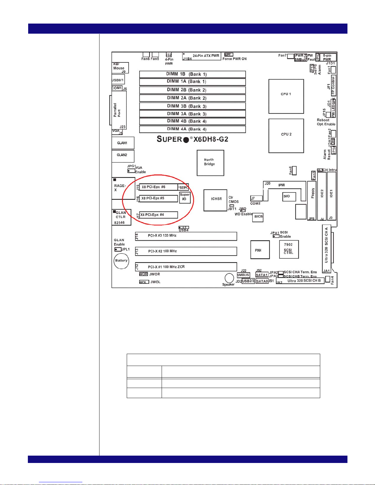
advantage of the PES64H16’s capabilities. One such system is the SuperMicro X6DH8-G2 motherboard
equipped with an Intel E7520 chipset which was introduced in 2004 to deploy dual-processor server chipset
technology. The board has three PCI Express slots. All slots have x8 connectors, but only two are electron-
ically connected for a x8 link width (J15 and J16). The remaining slots are electronically connected for a x4
link width configuration. Care must be taken to avoid using the EB64H16 in the x4 slot (J17). Figure 2.2
shows the proper connectors.
IDT Installation of the EB64H16 Eval Board
EB64H16 Eval Board Manual 2 - 3 January 16, 2007
Notes
Figure 2.2 SuperMicro X6DH8-G2 Motherboard
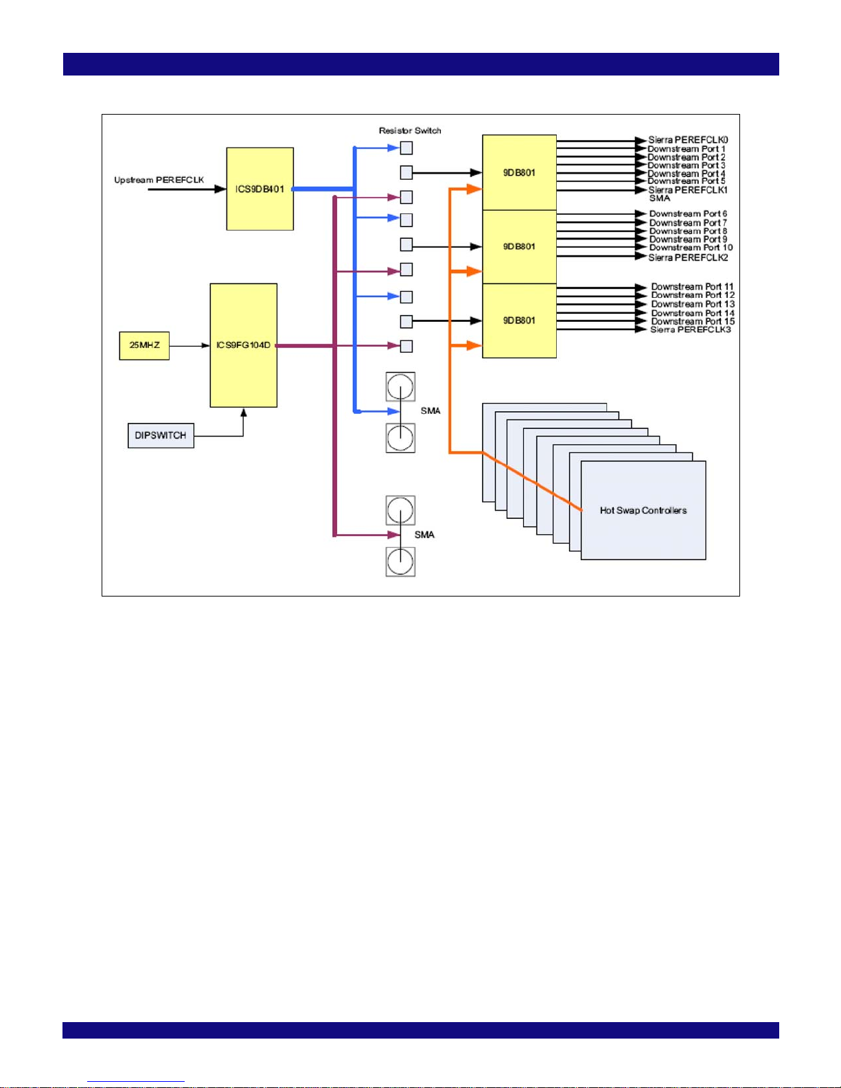
Reference Clocks
The PES64H16 requires four differential reference clocks. The EB64H16 derives these clocks from a
common source which is user-selectable. The common source can be either the host system’s reference
clock or the onboard clock generator. Selection is made by stuffing resistors described in Table 2.1.
Clock Configuration Stuffing Option
Install Clock Source
R36, R37 Onboard Reference Clock – Use onboard clock generator
R35, R148 Upstream Reference Clock – Host system provides clock (Default)
Table 2.1 Clock Source Selection

IDT Installation of the EB64H16 Eval Board
EB64H16 Eval Board Manual 2 - 4 January 16, 2007
Notes The source for the onboard clock is the ICS59FG104 clock generator device (U14) connected to a
25MHz oscillator (Y1). When using the onboard clock generator, the EB64H16 allows selection between
multiple clock rates and spread spectrum settings via DIP switches as described in Tables 2.2 and 2.3
respectively. Spread Spectrum technology reduces peak EMI emissions by modulating the frequency to
spread the peak energy over a wider bandwidth.
If the Clock Spread Spectrum is used to modulate data rate, then both ports must use same modulated
clock source. Therefore, if your system uses SSC, the on-board clock generator must be disabled and the
upstream reference clock must be used instead.
The output of the two onboard clock generator is accessible through four SMA connectors located on
the Evaluation Board. See Table 2.4. This can be used to connect a scope for probing or capturing
purposes and cannot be used to drive the clock from an external source.
Figure 2.3 illustrates the clock distribution block diagram for the EB64H16 evaluation board.
Clock Frequency Switch - S2[4:2]
S2[4] S2[3] S2[2] Clock Frequency
ON ON ON 100 MHz (Default)
ON ON OFF 125 MHz
ON ON ON <Reserved>
OFF OFF OFF <Reserved>
Table 2.2 Clock Frequency Selection
Clock Spread Spectrum Switch - S2[1]
S2[1] Spread
OFF No Spread (Default)
ON Spread Enable
Table 2.3 Clock Spread Spectrum Selection
Onboard Reference Clock Output (Differential) – J1, J3, J15, J8
J1, J15 Positive Reference Clock
J3, J8 Negative Reference Clock
Table 2.4 SMA Connectors - Onboard Reference Clock
IDT Installation of the EB64H16 Eval Board
EB64H16 Eval Board Manual 2 - 5 January 16, 2007
Figure 2.3 Clock Distribution Block Diagram
IDT Installation of the EB64H16 Eval Board
EB64H16 Eval Board Manual 2 - 6 January 16, 2007
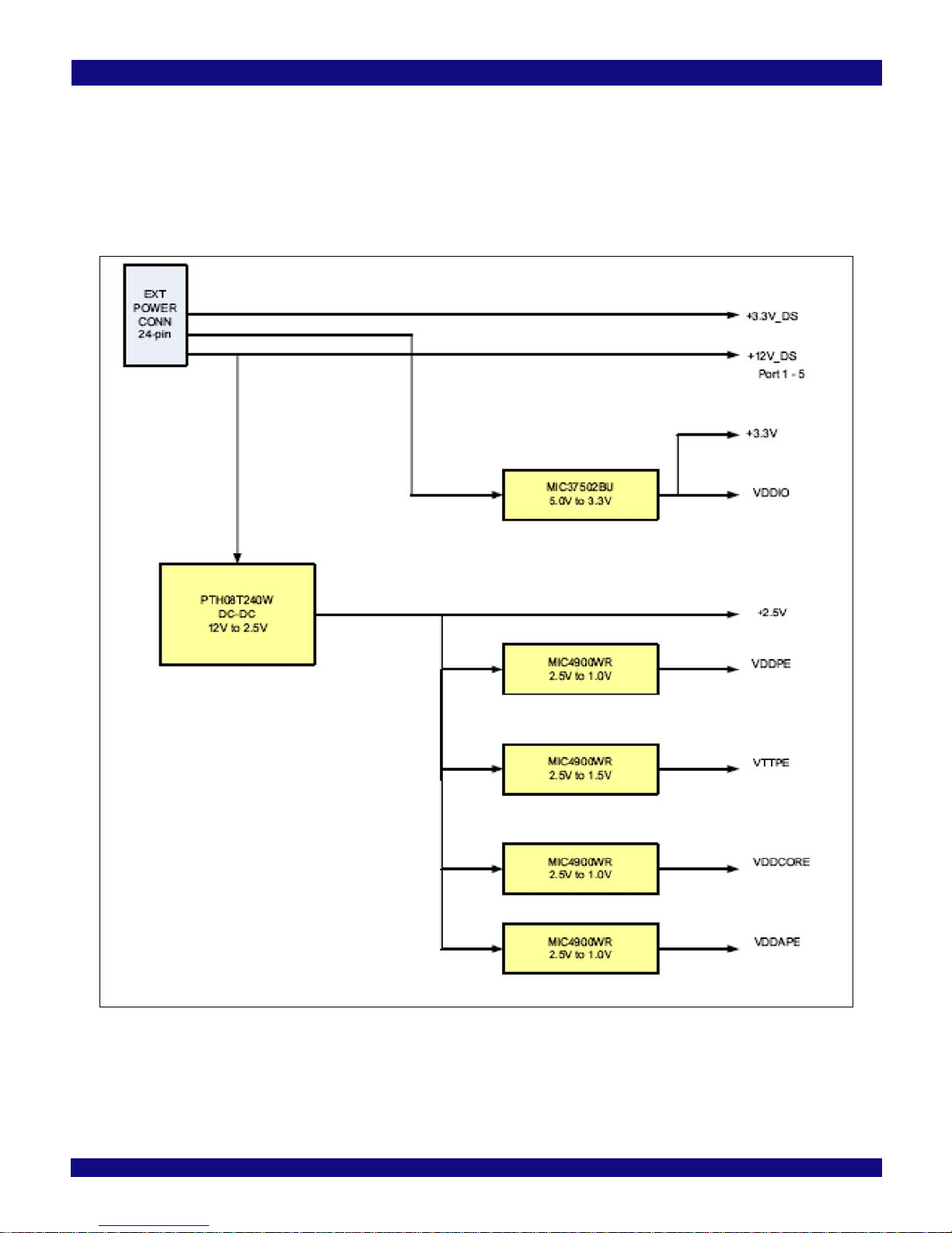
Power Sources
Power for the PES64H16 and all downstream ports is generated from the 12V from an external power connector. See Figure 2.4. A 12V to 2.5V DC-
DC converter is used to provide power to four LDO linear regulators to generate VDDCORE, VDDPEe, VDDAPE, and VTTPE voltages. The 2.5V from
the DC-DC converter is used to power the clock buffers. 3.3V is supplied form the power connector for VDDIO.
Figure 2.4 Power Distribution Block Diagram

IDT Installation of the EB64H16 Eval Board
EB64H16 Eval Board Manual 2 - 7 January 16, 2007
Notes The external power supply connectors are a 24-pin (J6) and an 8-pin (J5) molex connector as described
in Table 2.5 and Table 2.6. The +12V3 is used to power PES64H16 and downstream ports 1 through 5. The
+12V1 is used to power downstream ports 6 through 10. The +12V2 is used to power downstream ports 11
through 15.
The power on switch located at S3 can be used to control the supply power from the external power
supply connector. Add a shunt to W19 to enable power on switch.
Power Supply Minimum Load Connectors
To provide the minimum load requirement for each rail of the EPS12V supply, a 2-pin fan connector is
provided for connecting to an external power resistor for each rail.
Pin Signal Pin Signal
1 +3.3V 13 +3.3V
2 +3.3V 14 -12V
3GND15 GND
4 +5V 16 PS_ON
5GND17 GND
6+5V18 GND
7GND19 GND
8PWR_OK20 NC
9 5VSB 21 +5V
10 +12V3 22 +5V
11 +12V3 23 +5V
12 +3.3V 24 GND
Table 2.5 EPS12V 24_pin Power Connector - J6
Pin Signal Pin Signal
1 GND 5 +12V1
2 GND 6 +12V1
3 GND 7 +12V2
4 GND 8 +12V2
Table 2.6 EPS12V 8-Pin Connector - J5
Connector Supply Load Resistor Value
W157 3.3V 5.0 ohm
W158 5V 5.0 ohm
W100 12V1 25.0 ohm
W156 12V2 25.0 ohm
W159 12V3 25.0 ohm
Table 2.7 Minimum Load Connectors

IDT Installation of the EB64H16 Eval Board
EB64H16 Eval Board Manual 2 - 8 January 16, 2007
Notes PCI Express Serial Data Transmit Termination Voltage Converter
A DC-DC converter (U6) provides a 1.5V PCI Express serial data transmit termination voltage (VTT) to
the PES64H16.
PCI Express Digital Power Voltage Converter
A separate DC-DC converter (U7) provides a 1.0V PCI Express digital power voltage (VDDPE) to the
PES64H16.
PCI Express Analog Power Voltage Converter
A separate DC-DC converter (U28) provides a 1.0V PCI Express analog power voltage (VDDAPE) to
the PES64H16.
Core Logic Voltage Converter
A separate DC-DC converter (U1) provides the 1.0V core voltage (VDDCORE) to the PES64H16.
3.3V I/O Power Module
A separate DC-DC converter (U17) provides the 3.3V I/O voltage (VDDIO) to the PES64H16.
Power-up Sequence
The power-up sequence must be as following:
1. VDDIO - 3.3V
2. VDDCORE, VDDAPE, VDDPE - 1.0V
3. VTTPE - 1.5V
When powering up, each voltage level must ramp up and stabilize prior to applying the next voltage in
the sequence to ensure internal latch-up issues are avoided. There are no maximum time limitations
between sequential valid power level requirements.
Required Jumpers
To deliver power to the PES64H16 switch, the following jumpers must be shunted: W151, W152,
WW153, W154, W155. These jumpers were implemented so that the power consumption of the PES64H16
can be measured.
Heatsink Requirement
The PES64H16 with a maximum power dissipation of 13W will require a heatsink. The EB64H16 evalu-
ation board utilizes Molex heatsink with integrated fan.
Reset
The PES64H16 supports two types of reset mechanisms as described in the PCI Express specification:
–Fundamental Reset: This is a system-generated reset that propagates along the PCI Express
tree through a single side-band signal PERST# which is connected to the Root Complex, the
PES64H16, and the endpoints.
–Hot Reset: This is an In-band Reset, communicated downstream via a link from one device to
another. Hot Reset may be initiated by software. This is further discussed in the 89HPES64H16
User Manual. The EB64H16 evaluation board provides seamless support for Hot Reset.
This manual suits for next models
2
Table of contents
Other IDT Motherboard manuals

IDT
IDT ZMOD4510-EVK User manual

IDT
IDT P9242-R-EVK User manual

IDT
IDT 9FGV1005 Operating instructions

IDT
IDT ZMID520 Series User manual

IDT
IDT 9FGV1006 User manual

IDT
IDT 8A 72QFN Series User manual

IDT
IDT EB-LOGAN-23 User manual

IDT
IDT Tsi382 LQFP User manual

IDT
IDT 89EBPES16NT2 User manual

IDT
IDT P9242-G-EVK User manual

IDT
IDT 89EBPES12N3 User manual

IDT
IDT EVK-UFT285-6-7 User manual

IDT
IDT ADC1410S Series User manual

IDT
IDT VersaClock 6 5P49V69 Series User manual

IDT
IDT 8A34xxx 48QFN series User manual

IDT
IDT Tsi381 User manual

IDT
IDT ZWIR4532 User manual

IDT
IDT 82P33731 User manual

IDT
IDT 89EBPES16T4G2 User manual

IDT
IDT ZSSC4151 User manual


