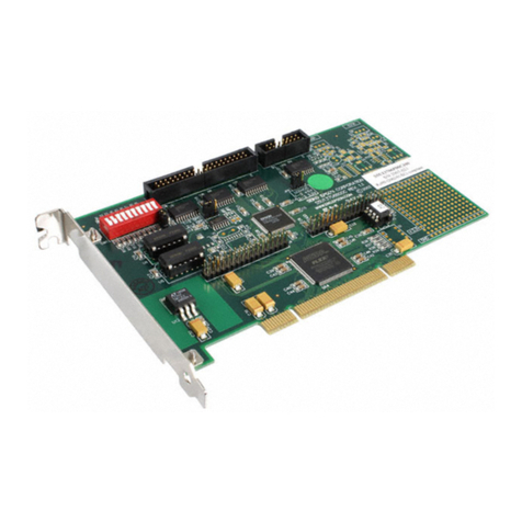
Intel EV80Cl96KB User manual

EV80Cl96KB
Evaluation Board
User’s Manual
(bier Number 270738-()O]

EV80C196KB Microcontroller Evaluation Board
Release 001
February 20,1989

Copyright 1989, Intel Corporation
Intel Corporation makes no warranty of any kind with regard to this material, including, but not limited
to, the implied warranties of merchantability and fitness for a particular purpose. Intel Corporation
assumes no responsibitlity for any errors that may appear in this document. Intel Corporation makes
no commitment to update nor to keep current the information contained in this document.
Intel Corporation assumes no responsibility for the use of any circuitry other than circuitry embodied
in an Intel product. No other circuit patents licenses are implied.
Intel software products are copyrighted by and shall remain the property of Intel Corporation. Use,
duplication, or disclosure is subject to restrictions stated in Intel’s Software License Agreement, or in
the case of software delivered to the U.S. government, in accordance with the software license
agreement as defined in FAR 52.227-7013.
No part of this document may be copied or reproduced in any form or by any means without prior
written consent of Intel Corporation.
Intel Corporation retains the right to make changes to these specifications at any time, without notice.
Contact your local sales office to obtain the latest specifications before placing your order.
The following are trademarks of Intel Corporation and its affiliates and may be used only to identify
Intel products:
376, Above, ActionMedia, BITBUS, Code Builder, DeskWare, Digital Studio, DVI, EtherExpress,
ETOX, ExCA, FaxBACK, Grand Challenge, i, i287, i386, i387, i486, i487, i750, i860, i960, ICE,
itBX, Inboard, Intel, lnte1287, lntel386, lntel387, lntel486, lntel487, intel inside., Intellec, iPSC,
iRMX, iSBC, ISBX, iWarp, LANprint, LANSelect, LANShell, LANSight, LANSpace, LANSpool,
MAPNET, Matched, MCS, Media Mail, NetPort, NetSentry, OpenNET, Paragon, PR0750,
ProSolver, READY-LAN, Reference Point, RMX/80, SatisFAXtion, Snapln 386, Storage Broker,
SugarCube, The Computer Inside., TokenExpress, Visual Edge, and WYPIWYF.
and the combinations of CCE,ICS, iRMX, ISBC, ISBX, iSXM, MCS, or UPI and a numerical suffix.
MDS is an ordering code only and is not used as a product name or trademark. MDS is a
registered trademark of Mohawk Data Sciences Corportation.
CHMOS and HMOS are patented processes of Intel Corp.
Intel Corporation and Intel’s FASTPATH are not affiliated with Kinetics, a division of Excelan,
Inc. or its FASTPATH trademark or products.
RBMis a registered trademark and AT is a trademark of International Business Machines, Inc.
Microsoft MS, MS-DOS, and XENIX are registered trademarks and Multiplan is a trademark
of Microsoft Corporation.
Addional copies of this manual or other Intel Literature may be obtained from:
Intel Corporation, Literature Sales
P.O. Box 7641
Mt. Prospect, IL 60056-7641
CONTENTS
SECTION Description ...................................... PAGE
INTRODUCTION ........................................................................................ 9
GETTING STARTED WITH THE EV80Cl96KB ........................................ 9
Powering the Board ........................................................................ 9
Connecting to your PC .................................................................... 9
Starting the Host Software .............................................................. 9
HARDWARE OVERVIEW OF THE EV80Cl96KB BOARD ...................... 10
Block Diagram of the EV80C196KB Board...................................... 10
Processor ........................................................................................ 30
Memory‘
............................................................................................ 10
Host Interface .................................................................................. 11
Digital I/O ........................................................................................ 11
Analog Inputs .................................................................................. 11
Decoding ........................................................................................ 12
Configuration Jumper Locations (Figure 3a) .................................. 14
Memory Configuration Jumper Locations (Figure 3b) .................... 15
Expansion Ports, Connectors and LEDs Locations (Figure 4) ........ 16
Host Serial Connector (Figure 5) .................................................... 17
8OCl96KB Serial Port Connector (Figure 6) .................................. 17
Analog Input Connector (Figure 7) .................................................. 18
I/O Expansion Connector (Figure 8) ................................................ 18
Memory-l/O Expansion Connector (Figure 9).................................. 19
Power Supply Connector (Figure 10) .............................................. 19
25pin to g-pin Adapter (Figure 11) ................................................ 20
INTRODUCTION TO iRISM-iECM96 SOFTWARE.. .................................. 21
Features .......................................................................................... 21
Restrictions ...................................................................................... 22
OVERVIEW ................................................................................................ 23
Embedded Controller Monitor.. ........................................................ 23
USER INTERFACE .................................................................................... 24
Background Information .................................................................. 24
Initiating and Terminating iECM-96 ................................................ 25
Default Base Commands ................................................................ 28

FILE OPERATIONS .................................................................................... 29
Loading and Saving Object Code .................................................... 29
Other File Operations.. ...................................................................... 30
PROGRAM CONTROL ................................................................................ 32
Resetting the Target ........................................................................ 32
Breakpoints ...................................................................................... 32
Program Execution .......................................................................... 33
Program Stepping ............................................................................ 35
DISPLAYING AND MODIFYING PROGRAM VARIABLES ........................ 37
Supported Data Types ...................................................................... 37
. BYTE Commands ............................................................................ 38
WORD Commands .......................................................................... 39
DWORD Commands ........................................................................ 40
REAL Commands ............................................................................ 41
STACK Commands .......................................................................... 42
STRING Commands ........................................................................ 42
Processor Variables .......................................................................... 43
ASSEMBLY AND DISASSEMBLY .............................................................. 44
Single Line Assembly Commands .................................................... 44
Disassembly Commands .................................................................. 45
SYMBOL OPERATIONS ............................................................................ 46
RISM .......................................................................................................... 47
RISM Variables 47
................................................................................
RISM Structure ................................................................................. 48
Receiving Data from the Host .......................................................... 48
Sending Datato the Host .................................................................. 48
RISM Commands .............................................................................. 49
Schematics and Parts List ..................................~.......~..................~......Appendix A
Specific iRlSM Information -..~.............~................................~..............0.. Appendix B
Listing of IRISM-196KB a.*.e..**..*...........*..
................................-....*.........aAppendix C
Timing Analysis .*-.................*..........e....
......................~........~....~.....~......~
Appendix D
Programmable Logic Equations ..........~...~....~.........~...........~.....~.........~..
Appendix E
Standard Memory-l/O Connector .....~......~................................~~.......~..~
Appendix F
Sample Session *“o...~~..~.....~..~.......e...~.*~.
...O.....................*s..*.............eo...Appendix G

-8- EV80C196KB Microcontroller Evaluation Board User’s Manual
Figure 1.
EV8OCl96KB Evaluation Board

EV80C196KB Microcontroller Evaluation Board User’s Manual -90
INTRODUCTION
The EV80C196KB is a next-generation version of the EV80C196KA. The major
changes are the use of a standard memory expansion bus compatible with the
EV80C51FB and EV80C186 boards, and the removal of the card edge bus. Also,
the HOLD/HLDA feature of the 8OC196KB is supported. The EV80C196KB is de-
signed to be a software evaluation tool for the ROMless 8OC196KB 16-bit microcon-
troller. As such, ports 3 and 4 are not available for use as I/O ports unless offboard
latches/buffers and decoding logic are used. All unreserved functions of the
80C196KB are available to you except for the Non-Maskable Interrupt (NMI), the
TRAP instruction, and 512 bytes of address space. The Chip Configuration Byte is
also used by the monitor, but most of its functions are provided by external logic.
GETTING STARTED WITH THE EV80C396KB
Powering up the Board
Power (+5, +/-12 Volts) must be connected to JP4 as shown on the board’s silk-
screen next to JP4 and in figure 10. Included with the board is a packet containing a
Molex connector and crimp terminals for your convenience.
Power supply requirements for the EV80C196KB board are as follows:
+ 5 VDC +I- 5 % @ 280 mA (150 mA if LED’sare disabled by
removing jumper shunt El 6)
+12VDC+/-20%@ 15mA
-12VDC+/-20%@ 15mA
Upon power-up (or after a reset) the board goes through initializations and a shift-
ing-pattern is displayed on the Port 1 LEDs when initialization has completed prop-
erly.
Connecting to your PC
Once you have applied power to the board, you need to connect Pl to a PC serial
port. Pl is configured to interface pin-to-pin with a standard nine-pin AT@)-type
serial connector (see figure 5 for pinout). Make certain that you use a cable provid-
ing all nine signals, as they are all needed for proper operation of the host interface.
When you have connected the cable, you may observe that the 8OC196KBis held in
reset, and all the LEDs turn on. This is because one of the host signals is used to
reset the part, and the signal’is often in a reset condition prior to invoking the host
software on your PC.
Note: if you have a 25pin serial port it will be necessary to make a 2%pin to 9-
pin adaptor (see figure 11 for details).
Starting the Host Software
After the you have made both connections to the board, you can invoke the host
interface. Install the disk in drive A of your system. At the DOS prompt type
“A:ECM96”eCR>. Your PC should eventually display the iECM-96 monitor screen.
If you have problems please refer to the sub-section “Initiating and Terminating
iECM-96” in the “USER INTERFACE” section of this manual. For further details on
using the monitor, refer to the “USER INTERFACE” section.

-IO- EV80C196KB Microcontroller Evaluation Board User’s Manual
HARDWARE OVERVIEW OF THE EV80C196KB BOARD
The EV80C196KB Microcontroller Evaluation board is delivered with an 8OC196KB,
8 K-words and 8 K-bytes of user code/data memory, a UART for host communica-
tions and analog-input filtering with a precision voltage reference. Also included is
programmable chip-select, bus-width and wait-state-counter logic which allows you
to custom tailor the board to look like your own system. The board’s physical dimen-
sions are 6 l/2” x 7 3/4” with an overall height of 3W. There are six main sections
to the EV80C196KB board: Processor, Memory, Host Interface, Digital I/O, Analog
Inputs and Decoding.
Block Diagram of the 80C196KB Board
Figure 2.
Processor
The Intel@)80C196KBis a 16-bit embedded microcontroller. Being a member of the
MCW-96 family, the 8OC196KB uses the same powerful instruction set and the
same architecture as the existing MCS-96 products. The 8OC196KB is an enhanced
CMOS version of the 8097BH. Its enhancements include up/down and capture
modes on Timer2, multiplyin
nearly twice as fast, Hold/Ho d Acknowledge logic, and power-down and idle modes
9 speeds almost 3 times as fast, overall execution
to save power. For more information, please refer to the 1989 “16-Bit Embedded
Controller Handbook,” Intel Corporation order number 270646-001 and the
8OC196KB Datasheet order number 270634-001.
Memory
There are five 28-pin memory sockets provided on the EV80C196KB board: Ul , U6,
U8, U13 and U14. The sockets are designed to support byte-wide, JEDEC-pinout,
memory devices of various types and sizes, i.e. 8K x 8 SRAM or 16K x 8 EPROM.
Ul and U8, U6 and U13 are connected as two 16-bit memory banks and U14 is
connected as an 8-bit memory bank.

EV80C196KB Microcontroller Evaluation Board User’s Manual -1I-
See appendix B and appendix C for details on reserved areas of memory.
Bank
No. Even
Bytes Odd
Bytes Enable
Signal Memory
Type
I.C. I.C.
0 U8 Ul CEO 8K x 16-bit Monitor EPROM
from 0-FFH and 1DOO-1DFFH
1 u13 U6 CEi 8K x 16-bit ROMsim/RAM
from 2000H-5FFFH
2 u14 u14 CE2 8K x 8-bit ROMsim/RAM
from 6000H-7FFFH
Host Interface
, The PC host interface is accomplished with the 82510 UART (U20) connected to Pl
via RS-232 drivers. The UART resides in the address range 1EOOH- 1EFFH.
Therefore, register 0 in the UART would be at address 1EOOHof the 8OC196KB,
reg. 1would be at 1EOl H, reg. 2 would be at 1E02H, etc. up to reg. 7 at 1E07H.
The registers will repeat again with reg. 0 at 1E08H due to the limited decoding
granularity of the EPLD. Pin 12 of the UART, OUTl#, is used to tell the PC host
when the 80C196KB is executing user code by a true level on the Ring Indicator
input of the host serial port.
Digital I/O
With the exception of the NMI input, which is used by the Host Interface, all Digital I/
0 functions of the 8OC196KB are available to you. There are eight LEDs on-board
along with buffer/drivers which allow you to quickly observe the state of Port 1,
HSO.0 and Port 2.5/PWM (see figure 4 or the schematics in appendix A for loca-
tion). The TxD and RxD pins of the 80C196KB (Port 2.0 and Port 2.1) are con-
nected to RS-232 buffer/drivers, which are connected to P2. All of the I/O signals
are available on JP2 (see figure 8 or the schematics in appendix A for pinout).
Note: because RxD is connected to an RS-232 receiver (U19 pin 3) any attempt
to use it as a digital input will result in a contention. If you would like to use it
as a digital input, remove jumper shunt El9 to disconnect the receiver.
Analog Inputs
The Port 0 inputs of the 80C196KB double as both digital and analog inputs. The
EV80C196KB board includes circuitry to make the analog inputs easier to use. A
precision voltage source for Vref is provided on board (U3 and U4) which can be
carefully adjusted by trimming RPl . Also, jumper shunt E4 allows Vref to be con-
nected to Vcc instead of the output of U3. By removing E4 entirely, an off board
reference can be connected to JPl . By removing jumper shunt E2, ANGND can be
isolated from Vss. Protective clamping diodes are installed on each channel. RC
networks are provided in sockets (to ailow you to change the input impedance to
match your application) on all of the analog input channels. If Port 0 is to be used

-729 EV80C196KB Microcontroller Evaluation Board User’s Manual
as a digital input, it is recommended that the capacitors be removed, and the resis-
tors replaced with wires. For additional connection information refer to figure 7 or
the schematics in appendix A. The ground and power planes beneath the analog
circuitry (Dl , D2, R3, C2, U3, U4, JPI and the analog connections on the
80Cl96KB) are isolated from the digital power and ground planes of the board to
keep noise from the analog inputs.
Decoding
The decoding logic on the EWOCl96KB board serves three purposes; to provide
Chip-Enable signals to memory and peripheral devices, to select the buswidth for
the device(s) being accessed and to provide wait-states for slow devices. This
section is provided in case you need to modify the memory configuration of the
EV80Cl96KB board. It is not necessary to understand this section for normal usage
of the board.
The heart of the decoding logic is U12, a 24-pin 5AC312 Intel EPLD or a C22VlO
programmable logic array which is socketed to allow easy changes. For the sake of
convenience it will be referred to as “the EPLD” throughout this text. The EPLD
uses latched addresses A8-Al5 along with CLKOUT, HLDA#, RESET# and STALE
(STretched ALE) from the 8OCl96KB as decode inputs.
There are 4 enable outputs from the EPLD, all of which are low-level true, however
only one should be true at a time to avoid bus contention. They are decoded from
the address lines, and an internally-latched signal called MAP. MAP is cleared
when the RESET# input is true, and set when the Monitor EPROMs are accessed in
the address range 1DOOH-IDFFH. MAP will always be set when the board is in the
USER mode.
pin 21 = CEO Enables memory in Ul and U8
(monitor EPROM as shipped).
CEO = (ADDRESS RANGE 2000H - 27FF and NOT MAP)
or ADDRESS RANGE OH- FFH
or ADDRESS RANGE 1DOOH- 1DFFH
pin 22 = CEl Enables memory in U6 and U13
(user 16-bit ROMsim/RAM as shipped).
CEl = (ADDRESS RANGE 2000H - 27FFH and MAP)
or ADDRESS RANGE 2800H - 5FFFH
pin 15-CE2 Enables memory in U14
(user 8-bit ROMsim/RAM as shipped).
CE2 = ADDRESS RANGE 6000H - 7FFFH
pin 14 - CS510 Enables U20, the 82510 UART, which is
used for host communications.
CS510 = ADDRESS RANGE 1EOOH- 1EFFH

EV80C196KB Microcontroller Evaluation Board User’s Manual 4 3-
The BUSWIDTH output of the EPLD, pin 16, is fed into the buswidth pin of the
8OC196KB. Therefore, it is driven low for accesses to 8-bit memory and high for
accesses to 16-bit memory. As shipped, it goes low simultaneously with CE2 or
CS510 as these are the only areas of memory mapped as 8-bit.
Programmed into the EPLD is a 3-bit wait-state machine clocked by the rising edge
of CLKOUT from the 8OC196KB. The transition sequence of the wait-state machine
is controlled by the current state of the machine and the inputs to the EPLD (for
further details see appendix E). While the bus of the 80C196KB is idle the wait-state
machine is locked in state 0, which is called async-start. The conditions for leaving
async-start are 1) ALE being asserted, 2) HLDA# not being asserted and 3) a
value on A8 - Al5 requiring wait-states. Because the falling edge of ALE can occur
before the next rising edge of CLKOUT can clock the wait-state machine, a signal
called STALE (for Stretched ALE) is used. STALE does not go low until after the
rising edge of CLKOUT.
During async-start, the output WAIT# from the EPLD is asserted asynchronously
based upon a value on A8-A15 requiring wait-states. If no wait-states are required,
WAIT# will not be asserted and the wait-state machine will remain in async-start.
However, if one or more wait-states are needed WAIT# will be asserted and the
wait-state machine will transition out of async-start on the next rising edge of
CLKOUT. The next state entered depends on how many wait-states are needed. If
only one is required the next state is remove&old, where WAIT# is deasserted
regardless of the inputs to the EPLD. If two watt-states are needed the next state is
hold-2, where WAIT# is always asserted, then the state after that is remove-hold.
The additional states, hold-3 - hold 7, work just like hold-2 with WAIT# always
asserted. The wait-state machine wJI count through from hold-2 to hold-n to
generate n wait-states before jumping to remove-hold to deassert WAIT#. The
maximum number of wait-states is seven.
The previous paragraph described how the signal WAIT# is generated based on the
rising edge of CLKOUT. However, the 8OC196KB needs to have a valid signal on
it’s READY input pin until the falling edge of CLKOUT. Therefore, it was necessary
to clock WAIT# through a negative-edge-triggered-JK flip-flop (U15A) by the falling
edge of CLKOUT to generate a signal called WAITN#. As inthe EPLD, WAITN# is
asserted asynchronously while ALE is high and WAIT# is asserted. After ALE goes
low WAITN# will remain asserted until WAIT# is deassetted and the flip-flop is
clocked. Besides the WAIT# signal, the WAITN# signal can be asserted by the
USEREADY signal from the expansion bus. As shipped, the EPLD has the following
configuration:
Memory Wait
Type States
ROMsim/RAM 0
ROMsim/RAM 0
Monitor EPROM 1
82510 UART 2
Unimplemented 0
Unimplemented 1
Enable
Signal
CEl
CE2
CEO
cs510
N/A
N/A
Memory Region
in User Mode
2000H-5FFFH
6000H-7FFFH
0-FFH, 1DOOH-DFFH
1EOOH-1EFFH
1OOH-1CFFH, COOOH-FFFFH
8000H - BFFFH

-14 EV8OC196KB Microcontroller Evaluation Board User’s Manual
- E4 Analog Voltage Reference Source
A-B AVref = VCC
B-i: AVref = U3/U4
__- Avref from JPl
E2 Analog Ground Reference
A-B AVss = Vss
--- Avss from JPl
E3 2000H-3FFFH Memory Location
A-B External
B-C Internal
E7 82510 UART Interrupt Signal to 8OC196KB
A-B UART Interrupt = EXTINnP2.2
B-C UART lnterrutp = NMI
El6 LED Driver Enable L E20 Enable RESET signal from host
A-B Enabled
i
1
A-B RESET from P2
__~ Disabled B-C RESET from Pl
-mm Reset circuit insolated
- E6 80C196KB CDE U5 pin 14 El1 HLDA# Input to PLD U12
A-B CDE = Vss A-B HOLD/HLDA feature in use
B-C CDE = Vcc --- HOLD/HLDA not used
El9 8OC196KB RXD signal from P2
A-B RXD driven by U19 pin 3
--- RXD can be used by JP2
Figure 3a.
Configuration Jumper Locations

EV80C196KB Microcontroller Evaluation Board User’s Manual -15
E8 U8 pin 27
A-B Pin 27 = Al 5
B-C Pin 27 = WRL#
E9 UlN8 pin 1
A-B Pin 1 = A15
B-C Pin 1 = Vcc
El0 Ul/U8 pin 26
A-B Pin 26 = Al 4
Pin27=A15
Pin 27 = WRH#
Pin27=A15
Pin 27 = WRH#
R-C Pin 26 = Vcc
El2 U13 pin 27 El7 U14 pin 26
A-B Pin27=A15
L
t
A-B Pin26=A13
B-C Pin 27 = WRL#k B-C Pin 26 = Vcc
El3 U6/U13 pin 1 El8 U14 pin 27
A-B Pin 1 =A15 A-B Pin27=A14
B-C Pin 1 = Vcc B-C Pin 27 = WR#
El4 U6/U13 pin 26 El5 U14 pin 1
A-B Pin26=A14 A-B Pin 1 =A14
B-C Pin 26 = Vcc Figure 3b. B-C Pin 1 = Vcc
Memory Configuration Jumper LocationiD Pin 1 =A15

-16- EV80C196KB Microcontroller Evaluation Board User’s Manual
/
DPl LED Array
1 P1.0
2 PI.1
3 P1.2
4 P1.3
5 P1.4
6 P1.5
7 P1.6
r JP2 input/Output Expansion Connector /
6 P1.7
9 P2.5/PWM#
10 HSO.O#
Ir
JPl Analog Input Connector
/ JP3 Memory-i/O Expansion Connector
L JP4 Power Connector Pl 82510 External UART Port-
P2 8OC196KB Internal UART Port-
Figure 4.
Expansion Ports, Connectors and LEDs

EV80C196KB Microcontroller Evaluation Board User’s Manual -17-
Pl Host Serial Connector
DB-9S RS232 Pin Host RS-232 Connection on
Nos. Signal Name Evaluation Board
5 (AB) SG Signal Ground
4 (CD) DTR Data Terminal Ready
3 @A) TxD Transmit Data
2 WV RxD Receive Data
1 W=) DCD Data Carrier Detect
Digital Ground
INIT thru E20-C
RxD of 82510
TxD of 82510
DTR Pl-pin 4
’
Pin
Nos. Host M-232
Signal Name Connection on
Evaluation Board
6 (CC)
7 (CA)
8 W
9 W
DSR Data Set Ready
RTS Request To Send
CTS Clear To Send
RI Ring Indicator
DTR Pl -pin 4
CTS Pl -pin 8
RTS Pl-pin 7
Run Indicator
P2 Serial Port Connector
DB-9S RS232
L
r
L
Figure 5.
Pin
Nos.
5 VW
4 (CD)
3 VW
2 W
1 (CF)
Host W-232
Signal Name
SG Signal Ground
DTR Data Terminal Ready
TxD Transmit Data
RxD Receive Data
DCD Data Carrier Detect
Connection on
Evaluation Board
Digital Ground
INIT thru E20-A
RxD of 8OC196KB
TxD of 8OC196KB
DTR P2-pin 4
Pin
Nos. Host M-232
Signal Mame Connection on
Evaluation Board
6 (CC)
7 GA)
8 W
9 W
DSR Data Set Ready
RTS Request To Send
CTS Clear To Send
RI Ring Indicator
DTR P2-pin 4
CTS PBpin 8
RTS PP-pin 7
No connection
Figure 6.

-189 EV80C196KB Microcontroller Evaluation Board User’s Manual
JPI Analog Input Connector
2x13 Pin MOLEX 39-51-2604 or Equiv.
ANGND - 1
VREF ---- 3
ANGND - 5
ANGND - 7
VREF ---- 9
ANGND -11
ANGND -13
VREF --- 15
ANGND -17
ANGND -19
VREF --- 21
ANGND -23
VREF --- 25
Figure 7.
JP2 I/O Expansion Connector
2x25 Pin MOLEX 39-51-5004 or Equiv.
1 thru 49 - VSS
2 - Analog Channel 0
4 -VREF
6 - Analog Channel 1
8 - Analog Channel 2
10 - VREF
12 - Analog Channel 3
14 - Analog Channel 4
16-VREF
18 - Analog Channel 5
20 - Analog Channel 6
22 - VREF
24 - Analog Channel 7
26 - ANGND
2 - Pl .OBi-directional
4 - Pl .l Bi-directional
6 - P1.2 Bi-directional
8 - P1.3 Bi-directional
10 - P1.4 Bi-directional
12 - Pl .YBREQ##Bi-directional
14 - Pl .G/HLDA#Bi-directional
16 - P1.7/HOLD# Bi-directional
18 - P2.0/Txd Output
20 - P2.1/Rxd Bi-directional
22 - P22/Extint Input
24 - P2.3fl2CLK Input
26 - P2.4fl2RST Input
28 - P2.5/PWM Output
30 - P2.6!T2UPDN Bi-directional
32 - P2.7/T2Capture Bi-directional
34 - HSO.0 Output
36 - HSO.l Output
38 - HS0.2 Output
40 - HS0.3 Output
42 - HSI.0 Input
44 - HSI.l Input
46 - HSl.2/HS0.4 Bi-directional
48 - HSl.3/HS0.5 Bi-directional
50 - vcc
Figure 8.

EV80C196KB Microcontroller Evaluation Board User’s Manual -19-
JP3 Memory-l/O Expansion Connector
2x30 Pin MOLEX 39-51-6004 or Equiv.
vcc __--------------- - 1
A0 Output ---------- 3
Al Output ---------- 5
A2 Output----------7
A3 Output ---------- 9
A4 Output --------- 11
A5 Output --------- 13
A6 output --------- 15
A7 Output---------17
vss _________-__------19
A8 output --------- 21
A9 Output --------- 23
Al 0 Output ------- 25
Al 1 Output ------- 27
Al 2 Output ------- 29
Al 3 Output ------- 31
Al 4 Output ------- 33
Al 5 Output ------- 35
vss _______----------- 37
CLKOUT Output - 39
RD# Output ------- 41
BREQ# Output --- 43
ALE Output ------- 45
NMI Input ---------- 47
RESET# Output - 49
No Connection --- 51
HLD4# Output --- 53
-12VDC ________-_--55
vss _____-_--------- -- 57
vcc ___------------ --- 59
r I
I
I
I
I
I
I
I
I
I
I
I
I
I
I
7cl
70
70
7u
70
30
3u
q u
q u
q u
q u
q u
q u
q u
q u
q u
q u
q u
q u
q n
q u
q u
q u
q u
q u
q u
q u
q u
q u
q u
2 - vcc
4 - DOBi-directional
6 - Dl Bi-directional
8 - D2 Bi-directional
10,- D3 Bi-directional
12 - D4 Bi--directional
14 - D5 Bi-directional
16 - D6 Bi-directional
18 - D7 Bi-directional
20 - vss
22 - D8 Bi-directional
24 - D9 Bi-directional
26 - DlO Bi-directioal
28 - Dl 1 Bi-directional
30 - D12 Bi-directional
32 - D13 Bi-directional
34 - D14 Bi-directional
36 - D15 Bi-directional
38 - Vss
40 - vss
42 - WR# Output
44 - BHE# Output
46 - UserReady Input
48 - INST Output
50 - P2.2/EXINT Bi-directional
52 - No Connection
54 - HOLD# Input
56 - +12VDC
58 - Vss
60 - Vcc
Figure 9.
JP4 Power Supply Connector
4 Pin MOLEX 26-03-3041 or Equiv.
Figure 10.

-2o- EV80C196KB Microcontroller Evaluation Board User’s Manual
To Evalboard
Note: Signal mneumonics are reference to the host.
To host PC
Figure 11.
25pin-to-g-pin Adapter

EV8OCI 96KB Microcontroller Evaluation Board User’s Manual -211
INTRODUCTION TO iRISM-IECM SOFTWARE
The EV80C196KB board uses an Embedded Controller Monitor (ECM) written for
the MCS-96 family of 16-bit microcontrollers. This monitor supports basic debug
facilities (LOAD, GO, STEP etc.) in the user’s target system. The ECM is broken
into two independent programs, one of these executes in the EV80C196KB (iRISM-
96KB) and the other executes in a IBM PC or BIOS compatible clone(iECM-96).
These two programs communicate via an asynchronous serial channel using a
binary protocol defined specifically for this application.
The partitioning of the ECM into two separate programs supports a number of goals
in the development of this system:
The system is easy to adapt to a new target because the code which runs in
the target is very simple and small.
The feature set of the user interface is not limited by the resources of the
target since the user interface is implemented in the host PC.
Concurrent operation of the ECM and the target system was easily achieved.
This allows you to interrogate and (carefully) modify the state of the target
system while it is running.
This manual section describes the user interface provided by the iECM-96, the
interface between this PC resident software and the target resident software, and
the structure of the software in the target. Appendix B lists the resources of the
80C196KB that are reserved for this RISM implementation. Appendix C is the listing
for the iRlSM software which runs in the 80C196KB on this board. It uses an Intel
82510 UART for host communications.
The iECM-96 was designed and implemented by Intel to support user’s of the MCS-
96 architecture, and is placed in the public domain with no restrictions or warranties
of any kind.
Features
Host system is an IBM PC AT, PC XT, or BIOS-compatible clone. (Interfaces
via COMl or COM2 at 9600 baud.)
Sixteen software execution breakpoints
Concurrent interrogation of target memory and registers
Supports BYTE, CHARACTER, WORD, STRING, DOUBLE-WORD and
FPAL-96 REAL variable types.
Single-Line Assembler/Disassembler
Symbolics compatible with Intel’s OMF debug records
Supports LOAD, SAVE, LIST, LOG, and command INCLUDE files.

EV80C196KB Microcontroller Evaluation Board User’s Manual
Restrictions
Two words of user stack are reserved for use by the iRISM-96 software.Other
memory and/or registers in the target memory will be used by the iRISM-96
software. The exact number and location of this memory is implementation
dependent. See appendix B or C for further information.
An asynchronous serial port capable of operation at 9600 baud must be
available in the target system. The RISM described in this document uses an
Intel 82510 UART. This version also uses the NMI (Non-Maskable Interrupt)
to signal that a received data character is available.
1 The TRAP instruction is reserved.
Breakpoints and program stepping will not operate if the user’s code is in
EPROM or other nonchangeable memory.
Table of contents
Other Intel Motherboard manuals

Intel
Intel DH61BE User manual

Intel
Intel D2500CC User manual

Intel
Intel DG41TY Configuration guide

Intel
Intel DP43BF User manual

Intel
Intel DQ67OW User manual

Intel
Intel iSBC 80 Quick user guide

Intel
Intel P45 Series User manual

Intel
Intel D945PAW User manual

Intel
Intel AN430TX - Motherboard - ATX Technical manual

Intel
Intel BLKDG965SSCK Configuration guide

Intel
Intel X38 User manual

Intel
Intel DH67BL User manual

Intel
Intel BOXDG35EC - Core2 Quad/LGA 775/ G35/FSB User manual

Intel
Intel DH61BE User manual

Intel
Intel Bay Trail Series User manual

Intel
Intel D915GLVG User manual

Intel
Intel CH-486-33A User manual

Intel
Intel MB899 User manual

Intel
Intel D925XECV2 User manual

Intel
Intel D945PLRN User manual