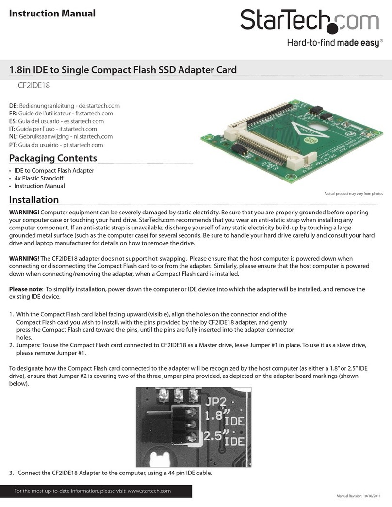
Intersil IM6100 Series User manual

INTERSIL
IM6100
CMOS
12
BIT
MICROPROCESSOR
D

CONTENTS
Introduction
............................................
3
Section
I:
IntersillM6100
CMOS
12
Bit Microprocessor
.................................
5
Introduction
......................................
6
Pin
Assignments
..................................
8
Specifications
....................................
9
Architecture
......................................
10
Memory
and Processor
Instructions
................
12
Operate
Instructions
...............................
14
Input/Output
Transfer
Instructions
..................
18
Internal
Priority
Structure
.........................
23
PDP-8/E
Compatibility
.............................
25
Applications
......................................
26
Section II: Intercept Prototyping System
................
29
Introduction
.........................
~
.....
'.' . . .
..
30
Specifications
.....................................
31
Intercept
Modules
.................................
32
Software
and
Hardware
Options
...................
34
Appendix
I-Edge
Connector
Pin
Assignments
.....
36
Section III: Intercept
Jr.
Tutorial System
.................
37
Section IV: Intersil Data Sheets
.........................
43
IM6101/6101A
CMOS
Parallel Interface
Element
.....
44
IM6312/6312A
CMOS
ROM, 1024
Word
x
12
Bit
......
59
IM6402/6403
CMOS/LSI UART
.....................
63
IM6508/6518
CMOS
RAM, 1024
Bit
.................
69
IM6508C/6518C
CMOS RAM, 1024
Bit
...............
75
IM6524/6524-1 CMOS RAM, 256
Bit
................
77
IM6551
16561
CMOS
RAM, 1024 Bit
.................
83
IM56S06/56S26
Electronically
Programmable
ROM 4096
Bit
....................................
87
8052/7101
31;2
Digit
AID
Pair
........................
89
8052A/7103A
41;2
Digit
Pair
.........................
97
Section V: CMOS RAM Reliability Report
...............
.105
1

2

3
INTRODUCTION
Since its
founding
on
July
26,
1967,
lntersil, Inc. has
become
a
company
of
many
products
and processes.
In
addition
to
the
digital CMOS devices
covered
in
detail
in
this
publication,
lntersil has developed
and
markets
a line
of
advanced linear
products
and
semiconductor
memories.
TTL
bipolar, MOS, metal-gate CMOS
and
silicon-gate CMOS processes
are
all
represented
in lntersil's line,
with
the
significant
design
advantage
that,
because
they
were developed
by
a single
forward-
thinking
company,
many
of
the
different
kinds
of
devices
and
technologies
produced
by lntersil will
work
together
for
enhanced
performance
and
greater
efficiency and flexibility
of
the
final
developed
product.
The
Silicon
Gate
CMOS process, which was
developed
at
lntersil over
two
years ago, offers a
semiconductor
structure
resulting in packing densities which surpass
the
conventional
metal gate process
3:
1.
Additionally,
circuit
performance
is
im-
proved 2: 1.
Mass
production
experience
with
the
Silicon
Gate
CMOS
process,
through
previously
announced
256
and
1024
bit
CMOS
RAMs, has lead
to
the
practicality
of
introducing
the
IM6100
microprocessor.
The
IM6100
and
IM6100A are single address,
fixed
word
length, parallel
transfer
microprocessors using 12-bit,
two's
com-
plement
arithmetic.
The
processors recognize
the
instruction
set
of
Digital
Equipment
Corporation's
PDP8/E
minicomputer.
The
internal
circuitry
is
completely
static
and
is
designed
to
operate
at
any
speed
between
DC
and
the
maximum
operating
frequency.
Two
pins are available
to
allow
for
an
external
crystal
thereby
el
iminating
the
need
for
clock
generators
and
level
translators.
The
crystal can be removed and
the
processor
clocked
by an
external
clock
generator.
A
12-bit
memory-accumulator
ADD
instruction
is
performed
in 5psec
by
the
IM6100 using a
+5
volt
supply
and
in
2.5psec
by
the
IM6100A
using a
+10
volt
supply.
The
device design
is
optimized
to
minimize
the
number
of
exter-
nal
components
required
for
interfacing
with
standard
memory
and peripheral devices.
lntersil
cannot
assume responsibility
for
use
of
any
circuitry
described
other
than
circuitry
entirely
embodied
in
an lntersil
product.
No
other
circuit
patent
licenses are implied. lntersil
reserves
the
right
to
change
without
notice
at
any
time
the
circuitry
and
specifications
of
any
Intersil
product
represented
in
this
document.

4

5
SECTION
I:
INTERSIL
IM6100
CMOS
12
BIT
MICROPROCESSOR

INTRODUCTION
IM6100
MICROPROCESSOR
Since its founding on July 26, 1967, INTERSIL INC. has offered
its customers advanced products utilizing the semiconductor indus-
try's most technologically sophisticated processes for the manufac-
ture of practical, economical devices.
The Silicon Gate CMOS process, which was developed at Intersil
in 1972, offers a semiconductor structure resulting in packing den-
sities which surpass the conventional metal gate process 3:1. Addi-
tionally, circuit performance is improved 2:1.
Mass production experience with the Silicon Gate CMOS proc-
ess, through previously announced 256 and 1024 bit CMOS RAMs,
has lead to the practicalityofintroducingthe IM6100 microprocessor.
6
The IM6100 is a single address, fixed word length, parallel trans-
fer microprocessor using 12-bit, two's complement arithmetic. The
processors recognize the instruction set of Digital Equipment Corpo-
ration's PDP8/E minicomputer. The internal circuitry is completely
static and is designed to operate at any speed between DC and the
maximum operating frequency.
Two
pins are available to allowfor an
external crystal thereby eliminating the need for clock generators
and level translators. The crystal can be removed and the processor
clocked
by
an
external
clock
generator.
A
12-bit
memory-
accumulator ADD instruction, using a +5volt supply, is performed in
5p,sec bythe IM6100, in 6p,sec by the IM6100C and in 2.5p,sec bythe
IM6100A using a +10 volt supply. The device design is optimized to
minimize the numberof external components required for interfacing
with standard memory and peripheral devices.

FEATURES
DESIGN
o Silicon Gate Complementary MOS
o Fully Static-O to 8 MHz
o Single Power Supply
IM6100/C
Vee=5
volts
IM6100A
Vee=10
volts
o Crystal Controlled
On
Chip Timing
o Low Power Dissipation <
10
mW @ 4 MHz @ 5 volts
o Single Power Supply 4V
~
Vee
~
11V
o TTL Compatible at 5 Volts
o Excellent Noise Immunity
o
-55°C
to +125°C Operation
INTERFACE
o
Memory-Any
Speed
o Control Panel
o Switch Register
o Asynchronous
CPU-Memory
and
CPU-Device
Communication
o 64 I/O Devices with PDP-8/E Compatible Interface
o Device Controlled Input-Output
o All Control Signals Produced By The CPU
o Power-on Initialize
ARCHITECTURAL
o Executes PDP-8/E, Instruction Set
o Direct, Indirect, and Autoindexed Memory Addressing
o 12-Bit Memory Accumulator ADD Instruction
IM6100 5fLsec @
+5
volts/4.0 MHz
IM6100A 2.5fLsec @ +10 volts/8.0 MHz
IM6100C 6fLsec @
+5
volts/3.3 MHz
o Input-Output Instruction
IM6100 8.5fLsec @
+5
volts/4.0 MHz
IM6100A 4.25fLseC @ +10 volts/8 MHz
IM6100C 10.2fLsec @
+5
volts/3.3 MHz
o Single-Clock, Single-Instruction Capability
o Direct Memory Access (DMA)
o Interrupt
o Dedicated Control Panel Features
APPLICATIONS
o Intelligent Computer Terminals
o POS Terminals
o Portable Terminals
o Aerospace/Satellite System
o Automotive Systems
o Remote Data Acquisition Systems
o Process Control
o Instrumentation
o Medical Electronics
o Displays
o Traffic Control
o Navigation
7

PIN
ASSIGNMENTS
;',
,',
<',
,
Data Field pin
phase
of.
indirectly addressed AND,
TAD, ISZ and DCA instructions so that
the data transfers are controlled by the
Data Field,
DF,
and not the Instruction
Field,
IF,
if
Extended Memory Control
hardware is used to extend the address-
ing space from
4K
to
32K
words.

SPECIFICATIONS
ABSOLUTE MAXIMUM RATINGS
Supply Voltage
Input or Output Voltage Applied
Storage Temperature Range
IM6100/C +4.0V to +7.0V
IM6100A +4.0V to 11.0V
GND
-0.3V
to
Vee
+0.3V
-65°C
to +125°C
Operating Temperature Range
Commercial
Industrial
Military
DC
CHARACTERISTICS
Vee
= 5.0V ±
10%
(IM6100), 10.0V ± 10% (IM6100A),
TA
= Commercial, Industrial or Military
PARAMETER
SYMBOL
CONDITIONS
MIN
TYP
Logical "1" Input Voltage V
IH
70%
Vee
Logical
"0"
Input Voltage V
IL
Input Leakage
IlL
OV
~
VIN
~
Vee
-1.0
Logical "1" Output Voltage V
OH2
10ur=0 Vee-O.
01
Logical "1" Output Voltage V
OH1
IOH=-0.2mA
2.4
Logical
"0"
Output Voltage V
OL2
lour
=0
Logical
"0"
Output Voltage V
OL1
10L
=1.6
mA
Output Leakage
10
OV
~
Vo
~
Vee
-1.0
Supply Current lec
Vee
= 5.0 volts
Vee
= 10.0 volts
CL= 50 pF;
TA
= 25°C
F
eLDeK
= Operating Frequency
Input Capacitance C
IN
5.0
.".
Output Capacitance
Co
8.0
ORDERING INFORMATION Circuit marking and product code explanation
9
Package-40
Pin Dip
Temperature Range
C-O°C
to 75°C
I
-40°C
to +85°C
M
-55°C
to +125°C
Version
Specific
Type
General Type Microprocessor
CMOS Process
INTERSIL, INC.
MAX
20%V
ee
1.0
GND +0.01
0.45
1.0
2.5
10.0
O°C
to +75°C
-40°C
to +85°C
-55°C
to +125°C
UNITS
V
V
/LA
V
V
V
V
p,A
mA
mA
pF
pF

ARCHITECTURE
The IM6100 has 6 twelve bit registers, a programmable logic
array, an arithmetic and logic unit and associated gating and timing
circuitry. A block diagram of the IM6100 is shown
in
Figure
1.
FIGURE
1
LINK
(1)
,......,.
___
-,
~L.;;L;.J..I_:..:r_~
o +5
()
GND
CRYSTAL
(2)
XTA,
XTB, XTC
DMAGNT,
,....--'----.1.--,
....-_--1_--1...,
INTGNT
IFETCH,
DATAF,
RUN
WAIT (40 PINS)
- - - INTERNAL CONTROL LINES
-EXTEHNAL INPUTS/OUTPUTS
-DATA
LINES
ACCUMULATOR (AC)
DX
(12)
RESET, RUN/HLT
DMAREQ,CPREO
INTREQ
(5)
---.,
I
I
I
I
I
I
I
I
I
I
I
I
I
____
J
SKP,
CO,
C1,
C2
The AC is a 12-bit register with which arithmetic and logical oper-
ations are performed. Data words may be fetched from memory to
the AC or stored from the AC into memory. Arithmetic and logical
operations involve two operands, one held in the
AC
and the other
fetched from the memory. The result of the operation
is
left
in
the AC.
The AC may
be
cleared, complemented, tested, incremented or
rotated under program control. The AC also serves
as
an
input-
output register. All programmed data transfers pass through the
AC,
LINK (L)
The Link
is
a 1-bit flip-flop that serves
as
a high-order extension
of the AC.
It
is used
as
a carry flip-flop for 2's complement arithmetic.
A carry out of the ALU complements the Link. Link can
be
cleared,
set, complemented and tested under program control and rotated as
part of the AC.
MQ
REGISTER (MQ)
The
MQ
is a 12-bit temporary register which
is
program accessi-
ble. The contents of AC may
be
transferred to the
MQ
for temporary
storage.
MQ
can
be
OR'ed with the AC and the result stored
in
the
AC.
The contents of the AC and the MQ may also
be
exchanged.
MEMORY ADDRESS REGISTER (MAR)
While accessing memory, the 12-bit MAR register contains the
address of the memory location that is currently selected for reading
or writing. The MAR is also used
as
an
internal register for micro-
program control during data transfers to and from memory and
peripherals.
PROGRAM COUNTER (PC)
The 12-bit
PC
contains the address of the memory location from
which the next instruction
is
fetched. During
an
instruction fetch, the 10
PC
is transferred to MAR and the
PC
is then incremented by
1.
When there
is
a branch to another address
in
memory, the branch
address
is
set into the
PC.
Branching normally takes place under
program control. However, during
an
input-output operation, a device
may specify a branch .address. A skip (SKP) instruction increments
the
PC
by
1,
thus causing the next instruction to
be
skipped. The
SKP instruction may
be
unconditional or conditional
on
the state of
the AC and/or the Link. During
an
input-output operation, a device
can also cause the next sequential instruction to be skipped.
ARITHMETIC AND LOGICAL UNIT (ALU)
The ALU performs both arithmetic and logical
operations-2's
complement binary addition, AND, OR and complement. The ALU
can perform a single position shift either to the left or to the right.
A double rotate
is
implemented
in
two single bit shifts. The ALU
can also shift
by
3 positions to implement a byte swap
in
two steps.
The AC is always one of the inputs to the ALU. However, under
internal microprogram control, AC may be gated off and all one's or
all zero's gated
in,
The second input may
be
anyone
of the other
registers under internal microprogram control.
TEMPORARY REGISTER (TEMP)
The 12-bit TEMP register latches the result of
an
ALU operation
before it
is
sent to the destination register to avoid race conditions.
The TEMP is also used
as
an
internal register for microprogram
control.
INSTRUCTION REGISTER (IR)
During an instruction fetch, the 12-bit
IR
contains the instruction
that
is
to
be
executed by the CPU. The
IR
specifies the initial step
of the microprogram sequence for each instruction and
is
also used
as
an
internal register to store temporary data for microprogram
control.
MULTIPLEXER (DX)
The 12-bit Input/Output Multiplexer handles data, address and
instruction transfers, into and out of, the CPU, from or into, the main
memory and peripheral devices
on
a time-multiplexed basis.
MAJOR
STATE
GENERATOR AND THE
PROGRAMMED LOGIC ARRAY (PLA)
During
an
instruction fetch the instruction to be executed is
loaded into the
IR.
The PLA
is
then used for the correct sequencing
of the CPU for the appropriate instruction. After
an
instruction
is
completely sequenced, the major state generator scans the internal
priority network. The state of the priority network decides whether
the machine is going to fetch the next instruction
in
sequence or
service one of the external request lines.
PLA OUTPUT LATCH
The PLA Output Latch latches the PLA output thereby permitting
the PLA to
be
pipelined; it fetches the next control sequence while
the CPU is executing the current sequence.
MEMORYANDDE~CECONTRO~
ALU AND REG TRANSFER LOGIC
The Memory and Device Control Unit provides external control
signals to communicate with peripheral devices (DEVSEL), switch
register (SWSEL), memory (MEMSEL) and/or control panel memory
(CPSEL). During I/O instructions this unit also modifies the PLA out-
puts depending
on
the states of the four device control lines
(SKP,
Co,
C1, C2
)·
The ALU and Register Transfer Logicprovides the control
signals for the internal register transfers
and
ALU operation.

TIMING AND
STATE
CONTROL
The IM6100 generates all the timing and state signals internally.
A crystal
is
used to control the CPU operating frequency. The
CPU
divides the crystal frequency by two. With a 4MHz crystal, the inter-
nal states will
be
of 500ns duration. The major timing states are
described
in
Figure
2.
T1
For memory reference instructions, a 12-bit address is
sent
on
the DataX,
DX,
lines. The Load External Address
Register, LXMAR,
is
used to clock
an
external register to
store the address information externally, if required. When
executing
an
Input-Output I/O instruction, the instruction
being executed is sent
on
the DX lines to
be
stored ex-
ternally. The external address register then contains the
device address and control information.
Various
CPU
request lines are priority sampled
if
the
next cycle
is
an
Instruction Fetch cycle. Current state of the
CPU is available externally.
T2 Memory/Peripheral data
is
read for
an
input transfer
(READ).
WAIT
controls the transfer duration. If WAIT
is
active during input transfers, the
CPU
waits
in
the
T2
state.
The wait duration
is
an
integral multiple of the crystal fre-
quency-250ns
for 4MHz.
For memory reference instructions, the Memory Select,
MEMSEL, line is active. For I/O instructions the Device
Select, DEVSEL, line
is
active. Control lines, therefore, dis-
tinguish the contents of the external register
as
memory
or device address.
External device sense lines,
Co,
C1, C2, and
SKP,
are
sampled if the
instruction
being executed is an I/O
instruction.
Control Panel Memory Select, CPSEL, and Switch
Register Select, SWSEL, become active low for data
transfers between the IM6100 and Control Panel Memory
and the Switch Register, respectively.
T3, T4•
Ts
ALU
operation
and
internal register transfers.
Ts
This state is entered for
an
output transfer (WRITE). The
address
is
defined during T1. WAIT controls the time for
which the Write data must
be
maintained.
FIGURE
2
CRYSTAL
FREQUENCY·!e
STATES
LXMAR
MEMIDEVISWICP
---+--.J
SELECT
XTB
\~------------------~I
XTC
-1
\~-----------------
IM6100 TIMING AND
STATE
SIGNALS
AC CHARACTERISTICS (TA =25°C), Derate 0.3% per
°C
PARAMETER
MajorStqteTime
LXMAR Pulse Width
·Addre~s$etupTi.f11e
Address Hold Time
r\GcessTimeFromLXMAR
Output Enable Time·
ReadPulse Width
Write Pulse Width
Data Setup Time
Data Hold Time
SYMBOL
tDH
IM6100
Vee
=
5.0
fe
=
4MHz
500
240
50
150
450
300
700
200
200
225
11
IM6100A
Vee
=
10.0
fe
= 8
MHz
IM6100C
Vee
=
5.0
fe
=
3.3MHz
UNITS

MEMORY
AND
PROCESSOR
INSTRUCTIONS
The
IM6100
instructions are 12-bit words stored in memory. The
IM6100 makes no distinction between instructions
and
data; it can
manipulate instructions
as
stored variables or execute data
as
instructions when it
is
programmed to do
so.
There are three general
classes of IM6100 instructions. They are referred to
as
Memory
Reference Instruction (MRI), Operate Instruction (OPR) and Input!
Output Transfer Instruction (lOT).
Before proceeding further,
we
will discuss the Specific Memory
Organization with which thelM6100 interfaces.
MEMORY ORGANIZATION
The IM6100
has
a basic addressing capacity of409612-bitwords.
The addressing capacity may
be
extended by Extended Memory
Control hardware. The memory system
is
organized
in
4096 word
blocks, called MEMORY FIELDS. The first 4096 words of memory
are
in
Field
O.
If a full 32K of memory
is
installed, the uppermost
Memory Field will
be
numbered
7.
In
any given Memory Field every
location has a unique 4 digit octal
(12
bit binary) address, 00008
to
77778
(000010
to 4095
10
).
Each Memory Field
is
subdivided into 32
PAGES of
128
words each. Memory Pages are numbered sequen-
tially from Page
OOe,
containing addresses
0000-0177a,
to Page 37e
,
containing addresses 7600e-7777e. The first 5 bits of a 12-bit
MEMORY ADDRESS denote the PAGE NUMBER and the low order
7 bits specify the
PAGE
ADDRESS of the memory location within
the given Page.
FIELD
7
PAGE
37,
PAGE
36,
FIELD 6
PAGE
35,
FIELDS.
PAGE
10,
FIELD 4
PAGE
07,
FIELD 3
PAGE
06,
PAGE
OS,
FIELD 2
PAGE
04,
PAGE
03,
FIELD 1
PAGE
02,
FIELD 0
PAGE
01,
PAGE
00,
7777,
LOC
177,
LOC
176,
LOC
175,
LOC010,
LOC007,
LOC
005,
LOC
004,
LOC
003,
LOC002,
f
LOC006,
~~~~:
I
~gg
~~~:
32K MEMORY
(10,FIELDS) 1MEMORY FIELD 1 MEMORY
PAGE
(40,
PAGES)
(200,
LOCATIONS)
MEMORY ADDRESS
I0 1 2 I3 4
1516
7
819
10
111
~
\
10
1
12
3
41
1516
7
819
10
111
PAGE
NUMBER
PAGE
ADDRESS
00
-37,
000-177,
12-BIT
OCTAL
MEMORY ADDRESS 4716,
1100111
do
0111
1:=£]
4 7 1 6
PAGE
NUMBER 1
0011
~
10011
~
23,
PAGE
ADDRESS 1001110
~
1001110
~
116,
MEMORY ORGANIZATION
During
an
instruction fetch cycle, the
IM6100
fetches the instruc-
tion pointed to
by
the
PC.
The contents of the
PC
are transferred to
the
MAR.
The PC is incremented
by
1.
The
PC
now contains the
address of the 'next' sequential instruction. The MAR contains the
address of the 'current' instruction which must
be
fetched from
memory. Bits 0-4
of
the MAR identify' the CURRENT PAGE, that
is,
the Page from which instructions are currently being fetched
and
bits
5-11
of the MAR identify the location within the Current
Page.
(PAGE ZERO (0), by definition, denotes the first
128
words
of memory,
OOOOe-Ol77
e.)
12
MEMORY REFERENCE INSTRUCTIONS (MRI)
The Memory Reference Instructions operate
on
the contents of a
memory location oruse the contents of a memory location to operate
on
the AC or the
PC.
The first 3 bits of a Memory Reference Instruc-
tion specify the operation code,
or
OPCODE,
and
the low order 9
bits, the OPERAND address,as shown
in
Figure
3.
o 2
FIGURE
3
3 4 5 6 7
L--t-INDIRECT
ADDRESSING
o
~
DIRECT
1 = INDIRECT
MEMORY PAGE
0=
PAGE 0
1 = CURRENT PAGE
8 9
MEMORY REFERENCE INSTRUCTION FORMAT
10
11
Bits 5 through
11,
the PAGE ADDRESS, identify the location of
the OPERAND
on
a given page, but they do not identify the page
itself. The page
is
specified
by
bit
4,
called the CURRENT
PAGE
OR
PAGE
0 BIT. If bit 4 is a
0,
the page address is interpreted
as
a -
location
on
Page
O.
If bit 4 is
al,
the page address specified
is
inter-
preted to be on the Current
Page.
For example, if bits 5 through
11
represent 123eand bit 4 is a
0,
the location referenced
is
the absolute address
0123
8. However, if bit
4 is a 1 and the current instruction
is
in
a memory location whose
absolute address
is
4610
ethe page address
123
e designates the
absolute address 4723e,
as
shown below.
4610
e =
100
110
001
000 = PAGE
10
011
=
PAGE
23
e
Location
4610
eis
in
PAGE
23e. Location 123e
in
PAGE
23e,
CURRENT
PAGE,
will be:
11001111
0100111= 100111 010011 = 4723e
i ,
PAGE PAGE
NUMBER
ADDRESS
238 1238
By this method, 256 locations may
be
directly addressed,
128
on
PAGE
0 and
128
on
the CURRENT
PAGE.
Other locations
are
ad-
dressed by utilizing bit 3. When bit 3 is a
0,
the operand address
is
a
DIRECT ADDRESS.
An
INDIRECT ADDRESS (pointer address)
identifies the location that contains the desired address (effective
address).
To
address a location that
is
not directly addressable, not
in
PAGE
0 or
in
the CURRENT
PAGE,
the absolute address of the
desired location
is
stored in one of the 256 directly addressable
locations (pointer address). Upon execution, the
MRI
will operate
on
the contents ofthe location identified
by
the address contained
in
the
pointer location.
It should be noted that locations
0010
e-0017e
in
PAGE
0 are
AUTOINDEXED. Ifthese locations are addressed indirectly, the con-
tents are incremented
by
1 and restored before they are used
as.
the operand address. These locations
may,
therefore,
be
used for
indexing applications.
Table
1lists the mnemonics for the five memory reference instruc-
tion, their OPCODE, the operations they perform, the number of
states
and
the execution time at +5.0V and +10.0V, assuming a
crystal frequency of 3.3MHz, 4MHz and 8MHz or a state time period
of 600ns, 500ns
and
250ns, respectively.

Notations applied
in
Table
1,
are defined as follows:
It
should be noted that the data is represented
in
Two's Comple-
ment Integer notation.
In
this system, the negative of a number is
formed by complementing each bit in the data word and adding
"1" to the complemented number. The sign is indicated by the most
significant bit.
In
the 12-bit word used by the IM6100, when bit 0 is
a "0", it denotes a positive number and when bit 0 is a "1", it denotes
a negative number. The maximum numberranges forthis system are
37778 (+2047) and 40008
(-2048).
( ) Denotes the contents of the register or location within the
parenthesis. (EA) is read as " ... the contents of the Effec-
tive Address".
DCA
JMP
« »Denotes the contents of the location pointed to by the con-
tents of the location within the double parenthesis.
«PA»
is
read as " ... the contents of the location pointed to by the
contents of the Pointer Aqdress."
<- Denotes" ... is replaced by ... "
1\
Denotes, logical AND operation
V Denotes, logical OR operation
BINARY ADD DIRECT (I =
0)
Operation: (AC)
<-(AC)
+ (EA)
TABLE
1
Description: Contents of the EA are ADD'ed with the contents ofthe AC
and
the result
is
stored in the AC; carry out
complements the
LINK.
If
AC
is initially cleared, this instruction acts
as
LOAD from Memory
BINARYADD INDIRECT (I =
1,
PA"# 0010-0017.)
Operation:
(AC)
<-(AC)
+ ((PA))
BINARY ADD AUTOINDEX (I = 1, PA = 0010-0017a)
Operation:
(PA)
<-(PA)+I;
(AC)
<-(AC)
+ «PA))
~TI·T'7.""C··:':
..•..
....
.•
SKIP IFZERODII::U:CT (I =
0)
. 0000" PC
<-,-PC
+ 1 .
.•
. .
,,"'"
'
'e)n.crennentec
by
1 and restored. If the result is zero,
the
nextsequential
'mSl[ruClI:on
IS,:sKlppeQ.:':T:,
','
'~;T:~,';T'
:T',T
~OINCHRI:Cl"(,
.1= 1, PA4.001Q-OQ17a
)'{
'-"".=
uuuu.
PC'~
" .
,+
~
';,
,""
,',
,:"i:,~;'{:0,~!,:,,:)'
,'(~'"
.-'~';';;;"''''''
NDEX
(1:= 1
,PA='cib10~001T
,;(:'
+<1'N·*J;«I?~\j)l::::..f~(PA))·
',1
;if
«PA))", 0000"
PC<-:--:!,~
t!'.;:i:'.i;;u.';'
3a DEPOSIT AND CLEAR THE ACCUMULATOR DIRECT (I =
0)
Operation:
(EA)
<-(AC);
(AC)
<-0000,
Description: The contents of the
AC
are stored in
EA
and the
AC
is cleared.
DEPOSIT AND CLEAR
THE
ACCUMULATOR INDIRECT(I = 1, PA
40010-0017
a
)
Operation: ((PA))
<-(AC);
(AC)
<-0000,
DEPOSIT AND CLEAR THE ACCUMULATOR AUTOINDEX(I =
1,
PA
= 0010-0017
a)
Operation:
(PA)
<-(PAl
+
1;
<-0000,
5.
JUMP DIRECT (I =
0)
Opemtion: (PC)
<-EA
Description: The next instruction
is
taken
from
the
EA.
JUMP INDIRECT(I =
1,
PA
4 0010-0017.)
Opemtion: (PC)
<-(PAl
JUMP AUTOINDEX (I = 1, PA = 0010-0017
a)
Opemtion:
(PA)
<-(PAl
+
1;
(PC)
<-(PAl
MEMORY REFERENCE INSTRUCTIONS
13
10
15
16
1,6
11
16
17
10
15
16
5.0
7.5
8.0
5.5
8.0
8.5
5.0
7.5
8.0
2.50
3.75
4.00
2.75
4.00
4.25
2.50
3.75
4.00
IM6100C
+5.0V
3.3MHz
6.0
9.0
9.6
6.6
9.0
10.2
6.0
9.0
9.6

OPERATE
INSTRUCTIONS
The Operate Instructions, which have
an
OPCODE of
78
(111),
consists of 3 groups of microinstructions. Group 1 microinstructions,
which are identified
by
the presence of a 0 in bit
3,
are used to
perform logical operations
on
the contents of the accumulator and
link. Group 2 micro instructions, which are identified by the presence
of a 1
in
bit 3 and a 0 in bit
11,
are used primarily to test the contents
of the accumulator and then conditionally skip the next sequential
instruction. Group 3 microinstructions have a 1
in
bit 3 and a 1 in
bit
11
and are used to perform logical operations
on
the contents
of
the AC and
MO.
The basic OPR instruction format is shown
in
Figure 4.
Operate microinstructions from any group may be microprogram-
med
with other operate microinstructions of the same group. The
actual code for a microprogrammed combination of two, or more,
microinstructions is the bitwise logical
OR
of the octal codes for the
individual microinstructions. When more than one operation
is
micro-
programmed into a single instruction, the operations are performed
in
a prescribed sequence, with logical sequence number 1 microin-
structions performed first, logical sequence number 2 microinstruc-
tions performed second, logical sequence number 3 microinstruc-
tions performed third and
so
on.
Two
operations with the same
logical sequence number, within a given group of microinstructions,
are performed simultaneously.
FIGURE
4
0 2 3 4 5 6 7 8 9 10
11
I1 : 1 : 1 I A : B I
MICROINSTRUCTION
An
GROUP 1 o -t
GROUP 2 1 0
GROUP 3 1 1
BASIC OPR INSTRUCTION FORMAT
i4

GROUP 1 MICROINSTRUCTIONS
Figure 5 shows the instruction format
of
a group 1 microinstruc-
tion.
Anyone
of bits 4 to
11
may be set, loaded with a binary
1,
to
indicate a specificgroup 1 microinstruction. If more than one of these
bits
is
set, the instruction
is
a microprogrammed combination of
group 1 microinstructions, which will be executed according to the
logical sequence shown
in
Figure
5.
FIGURE
5
o 2
BSW
IF
BITS
8 & 9
ARE
0
AND
BIT
10
IS
1.
LOGICAL
SEQUENCES:
1-CLA.CLL
2-CMA.CML
3-IAC
3 4
4-RAR,
RAL,
RTR,
RTL,
BSW
5 6 7 8 9
10
11
Table 2 lists commonly used group 1 microinstructions, their
assigned mnemonics, octal number, instruction format, logical
sequence, the operation they perform, the number of states and the
execution time at
+5.0Vand
+10.0V, assuming a crystal frequency
of 3.3MHz, 4MHz and 8MHz or a state time period of 600ns, 500ns
and 250ns, respectively. The same format is followed
in
Table 3 and
4 which correspond to group 2 and 3 microinstructions, respectively. GROUP 1 MICROINSTRUCTION FORMAT
RTR
SSW
CML
CMA
CIA
CLL
4
4
2
TABLE
2
OPERATION
RPTjI,TE
ACCU
MU
LATOR
LEF[
-The.
contents of the
AC
and Lare rotated one
I(osition.tothe left.
AC
(0)
is shifted
to
Land
L.is shifted
to
AC
(11).
ROTATE
TWO
LEFT
-The
contents
of
the
AC
and
L
are
rotated
two
binary positions to the left.
AC
(1)
is
Shifted
to
Land L is shifted
to
AC
(10).
ROTATE
ACCUMULATOR
RIGHT-The
content
of
the
AC
and
L are rotated one binary
position
to
the right.
AC
(11)
is
shifted
to
Land Lis shifted
to
AC
(0). .
ROTATE
TWO
RIGHT-The
contents
of
the
AC
and
L
are
rotated
two
binary positions
to
the
right.
AC
(to)
is
shifted
to
Land
L
is
shifted
to
AC
(1).
BYTE
SWAP-The
right six
(6)
bits
of
the
AC
are exchanged
or
SWAPPED
with the lett sixbits.
AC
(0)
is
swapped
with
AC
(6),
AC
(1)
with
AC (7),
etc.
L is
not
affected.
COMPLEMENT
LINK-The
content
of
the link
is
complemented.
COMPLEMENT
ACCUMULATOR-The
content
of
each bit
of
the
AC
is complemented
having
the
effect of replacing the content
of
the
AC
with
itson9's complement.
COMPLEMENT
AND
INCREMENT
ACCUMULATOR-The
content
of
the ACis
replaced
with
its
two's
complement. Carry out complements the
LINK.
CLEAR
LINK-The
link
is
loaded
with
abinary.O.
CLEAR
LINK-ROTATE
ACCUMULATOR
LEFT.
CLEAR
LINK-ROTATE
TWO
LEFT.
CLEAR
LINK-ROTATE
ACCUMULATOR
RIGHT.
CLEAR
LINK-ROTATE
TWO
RIGHT.
SET
THE
LINK-The
LINK
is
loaded
with
a binary 1corresponding
with
a microprogrammed
combination
of
CLL
and
CML.
CLEARAgCUMU
LATOR-The
accumulator
is
loaded
with
binary a's.
CLEAR
ACCUMULATOR-INCREMENT
ACCUMULATOR.
GET
TI-iE
IJNl)--,TheACisclea,red;theconlent
of
Lis shifted into AC(11),
This
i~a
rnicroprograrnmedcombirationofCLA
and
RAL.
GROUP 1 OPERATION MICROINSTRUCTIONS
15
EXECUTION
TIME
(MS)
NUMBER
IM6100
IM6100A
IM6100C
OF
+5.0V
+10.0V
+5.0V
STATES
4MHz
BMHz
3.3MHz
6.0
6.0
9.0
9.0
3.75 9,0
3.75 9.0
3.75 9.0

OPERATE
INSTRUCTIONS
CONTINUED
GROUP 2 MICROINSTRUCTIONS
FIGURE
6
Figure 6 shows the instruction format of group 2 microinstruc-
tions. Bits
4-10
may be set to indicate a specific group 2 micro-
instruction. If more than one of bits
4-7
or
9-10
is set, the
instruction is a microprogrammed combination of group 2 microin-
structions, which will
be
executed according to the logical sequence
shown in Figure
6.
o 2 3 4 5 6 7 8 9 10
LOGICAL SEQUENCES:
1 (Bit 8 is
Zero)-
SMA
or
SZA or SNL
(Bit 8 is One) -
SPA
and SNA and SZL
2
-CLA
3
-OSR.
HLT
Skip microinstructions may be microprogrammed with CLA,
OSR, or HLT microinstructions. Skip microinstructions which have a
oin bit
8,
however, may not be microprogrammed with skip micro-
instructions which have a 1 in bit
8.
When two or more skip micro-
instructions are microprogrammed into a single instruction, the
resulting condition
on
which the decision will be based is the logical
OR of the individual conditions when bit 8 is
0,
or,
when bit 8 is
1,
the decision will be based on the logical AND.
GROUP 2 MICROINSTRUCTION FORMAT
TABLE
3
OCTAL
MNEMONIC
CODe
OPERATION
SPA CLA 7710 1,2 SKIP ON POSITIVE ACCUMULATOR
THEN
CLEAR ACCUMULATOR 10 5.0 2.50
GROUP 2 OPERATE MICROINSTRUCTIONS
16
11
6.0

GROUP 3 MICROINSTRUCTIONS
Figure 7 shows the instruction format of group 3 microinstructions
which requires bits 3 and
11
to contain a
1.
Bits 4, 5 or 7 may be
set to indicate a specific group 3 microinstruction. If more than one
of the bits
is
set, the instruction is a microprogrammed combination
of group 3 microinstructions following the logical sequence listed in
Figure
7.
FIGURE
7
MNEMONIC
CLASWP
OCTAL
CODE
7721
LOGICAL
SEQUENCE
3
0 2 3 4 5 6 7 8 9 10
11
I1 : 1 : 1 I 1
CLA
>OAI
MO<
LOGICAL
SE~UENCE:
*Oon't Care
l-CLA
2-MOA.
MOL
3-ALL
OTHERS
GROUP 3 MICROINSTRUCTION FORMAT
TABLE
4
OPERATION
NUMBER
OF
STATES
NO
OPERATION-See
Group
1 Microinstructions 10
MQ
REGISTER
LOAD-The
content
of
the
AC
is
loaded
into
the
MO,
the
AC
is
cleared and the 10
original content of the
MQ
is lost.
MQ
REGISTER
INT9.A,.CCU~LJL}\"'9R-The
contentCl(lheMO.isOR·ed
with
the con-
tent
of
the
AC
and the resu.ltis 10adedintotre.AC,
T.he
Origin~1
cont~nt
of
\h~!lGislostbyt
theoriginal
content
of
the.MOisr~t~in~(j;Ihis.in~tr~ctio!)Pr8vi~!,,,tl)eprog"lrlJlT)er
withar.incl~sive.()R
operation.
SWAP
ACCUMULATOR
AND
MQ
REGISTER-The
content
of
the
AC
and
MO
are
interchanged accomplishing a microprogrammed combination
of
MOA
and
MOL.
CLEI)RI)CCtJMm.~1}c:5R
;
CLEAR
ACCUMULATOR
AND
MQ
REGISTER-The
content
of
the
AC
and
MO
are
loaded
with
binary
O's.
This
is
equivalent
to
a microprogrammed
combinalion
of
CLA
and
MOL.
CLEARAccofVjULAfORANClL.OACl
MOREGiSTER
INfbACdJfVjOCA-'
TOR
·.·.·Thi~i¢~ui~~le"tto.1).lT)i~rOh((Jgm~~~d·
D8mbin~tiOn
of.Gli\~n~MgA:'j
CLEAR
ACCUMULATOR
AND
SWAP
ACCUMULATOR
AND
MQ
REGISTER-The
content
of
the
AC
is
cleared. The content
of
the
MO
is
loaded
into
the
AC
and the
MO
is
cleared.
GROUP 3 OPERATE MICROINSTRUCTIONS
FIGURE
8
OPR2B
,
LXMAR
lfl
MEMSEL~~--~::::::j::::::::::::::t::::::::::::j
I
SWSEL:
I
DX I :
L.J
®
~%~~W~~~~~~~~~~
~~~
CD
® ®
CD
Instruction
Address
®
Instruction
~
CPU
®
Switch
Register.
~
CPU
Data
OSR INSTRUCTION TIMING
17
10
EXECUTION
TIME
(ILS)
IM6100
IM6100A
IM6100C
+5.0V
+10.0V
+5.0V
4.0MHz
8.0MHz
3.3MHz
5.0 2.50 6.0
5.0 2.50 6.0
5.0 2.50 6.0
5.0 2.50 6.0
5.0 2.50 6.0
5.0 2.50 6.0
5.0 2.50 6.0
5.0 2.50 6.0

INPUT/OUTPUT
TRANSFER
INSTRUCTIONS
(lOT)
The input/output transfer instructions, which have
an
OPCODE of
6a, are used to initiate the operation of peripheral devices and to
transfer data between peripherals and the IM6100. Three types of
data transfer may be used to receive or transmit information between
the IM6100 and one ormore peripheral I/O devices. PROGRAMMED
DATA
TRANSFER provides a straightforward means of communi-
cating with relatively slow I/O devices, such
as
Teletypes, cassettes,
card readers and CRT displays. INTERRUPT TRANSFERS use the
interrupt system to service several peripheral devices simultane-
ously, on
an
intermittent basis, permitting computational operations
to be performed concurrently with the data I/O operations. Both Pro-
grammed Data Transfers and Program Interrupt Transfers use the
accumulator as a buffer, or storage area, for
a"
data transfers. Since
data may be transferred only between the accumulator and the
peripheral, only one
12
bit word at a time may be transferred.
DIRECT MEMORY ACCESS, DMA, transfers variable-size blocks of
data between high-speed peripherals and the memory with a mini-
mum of program control required by the
IM6100.
lOT INSTRUCTION FORMAT
The Input/Output Transfer Instruction format, the numberof states
and the execution time at
+5.0V
and +10.0V, assuming a crystal
frequency of 3.3MHz, 4MHz and 8MHz or a state time period of
600ns, 500ns and 250ns, respectively is represented
in
Figure
9.
The first three bits, 0-2, are always set to 6a
(110)
to specify an
lOT instruction. The next six bits, 3-8, contain the device selection
code that determines the specific I/O device for which the lOT in-
struction is intended and, therefore, permit interface with up to
64
I/O
devices. The last three bits,
9-11,
contain the operation specification
code that determines the specific operation to be performed. The
nature of this operation for any given lOT instruction depends en-
tirely upon the circuitry designed into the I/O device interface.
PROGRAMMED DATA TRANSFER
Programmed Data Transfer is the easiest, simplest, most conven-
ient and most common means of performing data I/O. For micro-
processor applications, it may also be the most cost effective
FIGURE
9
o 2 3 4 5 6 7 8 9
10
11
lOT INSTRUCTION FORMAT
approach. The data transfer begins when the IM6100 fetches
an
instruction from the memory and recognizes that the current instruc-
tion is an
lOT.
This
is
referred to as IFETCH and consists of five (5)
internal states. The IM6100 sequences the lOT instruction through a
2-cycle execute phase referred to as
IOTA
and lOTs. Bits
0-11
of the
lOTinstruction are available
on
DX
0-11
at
IOTA' LXMAR. These bits
must be latched in an external address register. DEVSEL is active
low to enable data transfers between the IM6100 and the peripheral
device(s). Input-Output Instruction Timing
is
shown
in
Figure
10.
The selected peripheral device communicates with the IM6100
through 4 control
lines-Co,
C"
C2 and
SKP.
In the IM6100 the type
of data transfer, during
an
lOT instruction, is specified by the periph-
eral device(s) by asserting the control lines
as
shown in Table
5.
The control line
SKP,
when low during
an
lOT,
causes the IM6100
to skip the next sequential instruction. This feature
is
used to sense
the status of various signals
in
the device interface. The
Co,
C"
and
C2 lines are treated independently of the SKP line.
In
the case of a
RELATIVE or ABSOLUTE JUMP, the skip operation
is
performed
after the jump. The input signals to the IM6100, DX
0-11,
Co,
C"
C2,
and
SKP,
are sampled at
IOTA
during DEVSEL·XTc. The data from
the IM6100 is available to the device(s) during
DEVSEL·XT
c.
lOTs
cycle is internal to the IM6100 to perform the operations requested
during
IOTA'
Both
IOTA
and
lOTs
consist of six
(6)
internal states.
In
summary, Programmed Data Transfer performs data I/O with a
minimum of hardware support. The maximum rate atwhich program-
med data transfers may take place is limited by the IM6100 instruc-
tion execution rate. However, the data rate of the most commonly
used peripheral devices is much lower than the maximum rate at
which programmed transfers can take place in the IM6100. The
major drawback associated with Programmed Data Transfer is that
the IM6100 must hang
up
in a waiting loop while the I/O device com-
pletes the last transfer and prepares for the next transfer.
On
the
other hand, this technique permits easy hardware implementation
and simple, economical interface design. For this reason, almost
a"
devices except bulk storage units rely heavily on programmed data
transfer for routine data I/O.
EXECUTION
NUMBER
TIME
(ILS
OF
IM6100
IM6100A
IM6100C
STATES
+5.0V
+10.0V
+5.DV
4MHz
8MHz
3.3MHz
17
8.5
4.25
10.2
lOT NUMBER
OF
STATES/EXECUTION TIME
TABLE
5
CONTROL
LINES
OPERATION
Co
C,
C
2
L L PC
<-DEV
'Don't
Care
DESCRIPTION
:t~~;6oote~{0ftn~~Cis.
s'etlt,
tothed~vi~.i
The contentof the AC is sent to a device and then the AC is cleared.
i
tq~tli'i~
~ei~ly~gfr()rn
a~~SiG~;;gFi:~d'Wjih~hie'g~t~
irrth~f.<::ar(j
theresuitiisstor,i(fioih~,A.C.
i
REl:A'-i~E;.JUM,B··
Data is received from a device and loaded into the PC. This is referred to as an ABSOLUTE JUMP.
PROGRAMMED I/O CONTROL LINES
18

FIGURE
10
INTERNAL
STATES
1
IFETCH
, I
IOTA
~MARUl,--
________
~:n
1 -
~----------~--------------~
MEMSEL (L)
~.-------:----------------+:----------------i
1
~'----------------i
DEVSEL (L) : :
L-1
U :
DX(0.11)H
t§l
~~~~~
~
&~~~~
'~~~~",~~\~~\~
o ® @ @ ®
o INSTRUCTION ADDRESS @ DEVICE
DATA
IN,
CO,
C1,
C2, SKP
® INSTRUCTION ® AC OUT
@ DEVICE ADDRESS AND CONTROL
INPUT-OUTPUT INSTRUCTION TIMING
INTERRUPT
TRANSFER
PROGRAM INTERRUPT TRANSFERS
The program interrupt system may be used to initiate program-
med data transfers
in
such a way that the time spent waiting for
device status is greatly reduced or eliminated altogether.
It
also pro-
'ides a means of performing concurrent programmed data transfers
,etween the IM6100 and the peripheral devices. This is accom-
plished by isolating the I/O handling routines from the mainline pro-
gram and using the interrupt system to ensure that these routines
are entered only when
an
I/O device status is set, indicating that
the device
is
actually ready to perform the next data transfer, or
that it requires some sort of intervention from the running program.
The interrupt system allows certain external conditions
to
interrupt
the computer program
by
driving the INTREQ input to the IM6100
Low.
If
no
higher priority requests are outstanding and the interrupt
system is enabled, the IM6100 grants the device interrupt at the end
of the current instruction. After an interrupt has been granted, the
Interrupt Enable Flip-Flop
in
the IM6100 is reset so that no more in-
terrupts are acknowledged until the interrupt system
is
re-enabled
under program control.
FIGURE
11
EXECUTE INT IFETCH
INTERNAL
t=====J=======J======~
INT
EN
FF : 1
IFETCH , I
:@
~
________
~:n~
__
~==~
I
®
o ADDRESS 0000,
® DON'T CARE READ
@ PC WRITTEN IN LOC 0000,
@ ®
@ ADDRESS 0001,
® INSTRUCTION FETCH FROM 0001,
OFMEM
DEVICE INTERRUPT GRANT TIMING
19
DEVICE INTERRUPT GRANT TIMING
The current content of the Program Counter,
PC,
is deposited in
location 00008 of the memory and the program fetches the instruc-
tion from location
0001
8, The return address is available in location
00008, This address must be saved
in
a software stack if nested
interrupts
are
permitted. The INTGNT, Figure
11,
signal is activated
by the IM6100 when a device interrupt is acknowledged. This signal
is reset by executing any lOTinstruction as shown
in
Figure
12.
The
INTGNT signal is necessary to implement the Extended Memory
Control hardware when more than 4K of memory
is
required. The
INTGNT is also useful in implementing
an
External Vectored Priority
Interrupt network.
The user program controls the interrupt mechanism of the IM6100
by
executing the processor lOT instructions listed
in
Table
6.
Several
of these interrupt lOT instructions are also used if the memory is
extended beyond 4K words.
STATES
1
1
IFETCH I
10
FIGURE
12
IFETCH
IOTA
~MAR
lI1'--
________
~
L----------.;.-----------i
1
MEMSEL(L)
~
,
I I
DEVSEL (L)
!..,
-----------:.---.~r----...,@r.,---------------:
, 1
INTGNT I
IL.
____________
---..:
o INSTRUCTION ADDRESS @
DATA
TRANSFER FROM PERIPHERAL DEVICES
® 6XXX FROM MEMORY AS CONTROLLED BY
Co,
C"
AND
C,
@ ADDRESS 6XXX ®
DATA
TRANSFER TO PERIPHERAL DEVICES
AS CONTROLLED BY
Co,
C"
AND
C,
DEVICE INTERRUPT GRANT RESET TIMING
This manual suits for next models
2
Table of contents
Other Intersil Computer Hardware manuals
Intersil
Intersil ISL71218MEVAL1Z User manual
Intersil
Intersil ISL39000C User manual

Intersil
Intersil ISL37305P User manual

Intersil
Intersil ISL37105P User manual

Intersil
Intersil ISL6423B User manual

Intersil
Intersil HIP6302EVAL1 Installation and operating instructions
Intersil
Intersil ISL705ARH User manual

Intersil
Intersil ISL37101P User manual
Intersil
Intersil ISL37106P User manual

Intersil
Intersil CDP1802BCE User manual